Coherent transport in Nb/-doped-GaAs hybrid microstructures
Abstract
Coherent transport in Nb/GaAs superconductor-semiconductor microstructures is presented. The structures fabrication procedure is based on -doped layers grown by molecular-beam-epitaxy near the GaAs surface, followed by an As cap layer to protect the active semiconductor layers during ex situ transfer. The superconductor is then sputter deposited in situ after thermal desorption of the protective layer. Two types of structures in particular will be discussed, i.e., a reference junction and the engineered one that contains an additional insulating AlGaAs barrier inserted during the growth in the semiconductor. This latter configuration may give rise to controlled interference effects and realizes the model introduced by de Gennes and Saint-James in 1963. While both structures show reflectionless tunneling-dominated transport, only the engineered junction shows additionally a low-temperature single marked resonance peaks superimposed to the characteristic Andreev-dominated subgap conductance. The analysis of coherent magnetotransport in both microstructures is successfully performed within the random matrix theory of Andreev transport and ballistic effects are included by directly solving the Bogoliubov-de Gennes equations. The impact of junction morphology on reflectionless tunneling and the application of the employed fabrication technique to the realization of complex semiconductor-superconductor systems are furthermore discussed.
I Introduction
Heterostructures represent nowadays the most dynamic and rapidly growing field of semiconductor research. This success derives in particular from the great freedom they offer in the design of material energy-band diagram. With respect to bulk structures these additional possibilities come from the addition of two basic elements: the opaque barrier, exploited to realize quantum well and other reduced-dimensionality systems, hot-electron injectors and several heterojunction transistors, and the thin barrier, exploited to obtain the tunnel effect (both resonant and non resonant), and superlattices. The present work experimentally addresses the addition a a further element, i.e., the superconducting barrier (S). This allows the introduction of an entirely new effect in the physics of the heterostructures, i.e., the Andreev reflection andr . This process allows the control of the nature and the phase of quasi-particles in the heterostructure: an electron injected from the normal region (N), in the present case a degenerate semiconductor (Sm), with energy lower than the superconducting gap can not propagate as a single particle in the superconductor but can be reflected as a phase-matched hole in the Fermi sea of the N region, while at the same time a Cooper pair is transmitted in the superconductor. The reflected quasi-particle phase is controlled by the superconductor condensate. All this has to be contrasted to normal reflection present also in non-superconducting heterostructures.
Thanks to Andreev reflection, dissipative currents in the normal portion of the structure are converted in dissipationless supercurrents inside the superconductor, thus allowing electric transport through the whole system. Moreover, due to its two-particle nature, Andreev reflection is strongly affected by the NS interface transmissivity. High transparency is therefore required to observe this effect and of the associated coherent phenomena. The art of controlling the interface quality, in particular in the case of hybrid SmS microstructures, is still nowadays a challenging task and much effort has to be devoted to its optimization giaz1 . Achieving high interface transparency in SmS contacts, however, is hindered by the presence of interface oxide layers and Schottky barriers, and by the difference in Fermi velocities in the S and Sm layers blonder . In order to avoid Schottky barrier formation, several authors have chosen InAs for the realization of hybrid devices. The main transparency-limiting factor in this case is interface oxidation/contamination and several methods have been explored to limit its impact kr ; tak ; lach . InAs, however, is not the Sm of choice for heterostructure growth and GaAs- or InP-based systems are much more widespread and versatile. For these latter materials Schottky barriers are the dominant factor in limiting transparency.
In this paper we shall focus on some experimental results obtained on Nb/-doped-GaAs hybrid microstructures fabricated with a versatile and reproducible technique. GaAs is, after Si, probably the most widespread semiconductor material and at the basis of a well developed nanotechnology. Its main peculiarities are a low effective mass value () that favours high bulk mobilities, and the feature that a replacement of part or all of the Ga atoms by Al atoms causes a negligible change in its lattice constant. This leads to GaAs/AlGaAs interfaces with highly reduced defect densities and in nearly perfect barriers for electron confinement. The resulting two-dimensional electron gas may yield mean free path of several tens of microns, making the GaAs/AlGaAs system the best candidate for the realization of non-superconducting nanostructures in the ballistic limit. These remarkable peculiarities, however, can not easily be exploited for SmS applications due to the already mentioned presence of the Schottky barrier that may strongly hinder the manifestation of Andreev reflection. Nevertheless, GaAs can still be employed with superconductors by heavily doping the semiconductor surface layers in order to achieve high interface transmissivity (this technique is commonly referred to as -doping technique) kast ; tab . This is indeed a practical and effective way to use GaAs in the contest of SmS structures avoiding annealed superconducting contacts gao ; mar , and will be demonstrated in the following. More in particular, we shall examine two Nb/-doped-GaAs microstructures, that will be referred to as the SN reference giaz2 and the SNIN engineered giaz3 structure. The latter differs from the reference junction for the additional presence of an Al0.3Ga0.7As barrier inserted during the growth process.
The paper is organized as follows. In Section II we shall describe the structures characteristics and some details of the employed fabrication technique. The electrical behavior of the SN reference junctions will be addressed in Section III, where we will demonstrate the observation of reflectionless tunneling(RT)-dominated transport. Such results will be discussed within a random matrix approach. We shall report here the effectiveness of the employed fabrication protocol for the implementation of more complicated systems, i.e., the SNIN engineered junctions. In Section IV we shall present the experimental evidence in these latter structures of resonant states induced by the presence of the AlGaAs insulating barrier. The observed behavior is of the de Gennes-Saint-James type and reveals how it is possible to tailor these semiconductor heterostructures in order to observe coherent transport effects. The electrical behavior of these junctions will be described within a random matrix formalism and ballistic effects will be included directly solving the Bogoliubov-de Gennes equations in a model potential profile. Our description of the system is confirmed by the observed temperature and magnetic-field dependence. The conclusions and some additional remarks will be given in Section V.
II Samples fabrication and experimental details
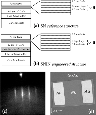
For the semiconducting portion of the SN reference structure (see Fig. 1(a)), a 200-nm thick n-GaAs(001) epilayer (nominal Si doping n = 4.7 cm-3) was initially grown by molecular beam epitaxy (MBE) on an undoped GaAs buffer and a semi-insulating GaAs(001) wafer. This was followed by the growth of 15 nm of GaAs doped by a sequence of five layers (nominal Si concentration cm-2 per layer) spaced by 2.5 nm. The semiconductor portion of the SNIN engineered structure (see Fig. 1(b)), instead, consists of a 1 m thick -GaAs(001) buffer layer Si-doped nominally at cm-3 grown by MBE on a -GaAs(001) substrate, followed by a 4 nm thick Al0.3Ga0.7As barrier. This was followed by the growth of a 12 nm thick GaAs(001) epilayer Si-doped at cm-3 and by 14 nm of GaAs doped by a sequence of six Si -doped layers spaced by 2 nm. The thickness of the GaAs epilayer sandwiched between the superconductor and the AlGaAs barrier was selected in order to have an experimentally-accessible single quasi-bound state below the superconductive gap, and the Si -doped layers at the Nb/GaAs interface were employed to achieve the required transmissivity. A similar doping scheme was successfully used by Taboryski and co-workers to lower the contact resistance in fully-MBE-grown Al/GaAs(001) junctions tab . The choice of in-situ junction formation, however, severely limits the superconductor materials usable. In our case, on the contrary, following the growth of the top -doped GaAs layer, a 1-m-thick amorphous As cap layer was deposited at -20∘C on both structures to protect the surface during transfer in air to an ultra-high-vacuum (UHV) sputter-deposition/surface analysis system (the typical base pressure of the UHV fabrication system is about Torr). The samples where then heated at about 400∘C to desorb the cap layer in order to achieve a sharp GaAs(001) 2 4 reflection-high-energy-electron-diffraction (RHEED) pattern. An example of the corresponding RHEED pattern image obtained on the SN reference structure is shown in Fig. 1(c). The RHEED pattern of the SNIN engineered junction appeared quite similar. Nb overlayers 100-nm-thick were fabricated in situ by dc-magnetron sputter-deposition at a deposition rate of 3.5 nm/s. Moreover, substrate temperature during Nb deposition was kept at 200 ∘C to promote film adhesion. Typical 100-nm-thick Nb films displayed a transition temperature of 9.28 K and a residual resistivity ratio at 10 K (RRR10) as high as 60 (data not shown).
Rectangular 100160 m2 Nb/GaAs junctions were patterned by standard photolithographic techniques and reactive ion etching (RIE) using a CF4+O2 gas mixture. Two additional 9045 m2 Ti/Au bonding pads were e-beam evaporated on top of each Nb contact to allow 4-wire measurements (Figure 1(d) shows the scanning electron micrograph of one of the measured devices). In the case of SN reference junctions, the electrical characterizations were performed with two leads on the Nb electrode under interest and the other two connected to two separate neighboring contacts located symmetrically with respect to the junction considered. In this way our conductivity data reflect only the junction properties with no influence from the series resistance of the semiconductor film. We have also experimentally determined the influence of the leakage paths around the contacts by removing the semiconductor layer above and below the contact strip (“contact-end test structure” sch ). The correction to the contact resistance appeared to be negligible on the scale relevant to the experiment. For what concerns SNIN devices, differently, 4-wire measurements were performed with two leads on the junction under study and the other two connected to the sample back contact, thus allowing to probe the vertical transport characteristic intrinsic to the structure.
Magnetoconductance measurements of the junctions were performed in a closed-cycle 3He cryostat equipped with a superconducting magnet from 0.3 K to temperatures larger than , and current-driven measurements were performed employing a high-resolution current source. Furthermore, in order to preserve any sharp features in the junction characteristics, special care was taken in data acquisition using low measurements speed and small current stepwidths.
III SN reference junctions: reflectionless tunneling-dominated transport

In order to determine carrier concentration and Hall mobility of the SN reference structure a portion of the semiconductor was not Nb coated and, following As desorption, it was patterned into Hall bars by removing the entire epilayer. At 0.34 K we obtained cm-3 and cm2/V s. From these values it was possible to estimate electron mean free path ( nm) and thermal coherence length at = 0.34 K, m, where cm2/s is the three-dimensional diffusion constant. Additionally, the single-particle phase coherence length, m, was also estimated from weak localization magnetoresistance measurements, following Ref. kut .
Figure 2(a) shows a typical set of differential-conductance bias characteristics () of one of the junctions measured at various temperatures in the 0.34 - 1.00 K temperature range. The symmetry of the characteristics together with the large value of the conductivity at low bias at the lowest temperatures are a clear indication of the transparency of the Nb/GaAs junctions fabricated (see also the inset of Fig. 2(a) where the conductance spectrum at 0.34 K up to biases well above the superconducting energy gap is plotted). The fabrication procedure adopted yielded an excellent contact-to-contact uniformity leading to characteristics reproducible within few % in all the junctions measured. The data display the typical behavior of a diffusive non-tunnel SmS junction. In particular, at the lowest temperatures measured, a marked peak is observed in the differential conductance spectrum at zero bias. As we shall argue, this is the direct manifestation of reflectionless tunneling (RT) kast ; marmor ; ben1 ; RT is indeed known to be due to constructive interference of quasiparticles coherently backscattered withing the diffusive region towards the SmS interface barrier wees . This effect gives rise to a sizable enhancement of conductivity around zero-bias, and its coherent nature makes it very sensitive to electric and magnetic fields and to the temperature. Furthermore, it will be very useful for the analysis of the junction properties.

In fact it is not straightforward to obtain reliable junction parameters by studying the Andreev pattern in diffusive junctions giaz4 ; neu . On the contrary, when one such zero-bias conductance peak (ZBCP) is observed in these systems, much information can be obtained by examining its intensity and its temperature and magnetic-field dependence marmor ; ben1 . The temperature dependence of the RT zero-bias enhancement is shown for clarity in Fig. 2(b), while Figure 2(c) shows the normalized zero-bias conductance dependence ( is the junction normal state resistance) in the whole temperature range up to Nb critical temperature. With the exception of the low temperature range, where the RT enhancement persists, this behavior is that one expected for a junction in the diffusive regime.
The electrical properties of our junctions can be analyzed within the random matrix theory of phase-coherent Andreev reflection proposed by Beenakker ben2 . He studied a model-junction consisting of a normal and a superconductor reservoirs linked by a disordered normal-metal region of length and width . Between this disordered region and the superconductor reservoir the model-system includes a potential barrier characterized by a mode-independent transmission probability (). In this system, under appropriate conditions an enhanced conductivity around zero bias was predicted to occur with respect to the classical Andreev reflection behavior leading to a ZBCP. The width of the latter (i.e. the bias voltage at which the RT correction to the conductivity vanishes) is given by , where is the Fermi velocity in the normal region. Furthermore, upon application of a magnetic field ZBCP is suppressed for field intensities larger than . In real systems, at finite temperatures, and are to be replaced by , if it is smaller marmor ; ben1 . In order to analyze our data within this model, we can first of all determine the experimental value of by examining the data in Fig. 3(a) where the evolution of the ZBCP is well displayed thanks to the limited influence of the in-plane magnetic field on the classical conductivity. The RT correction persists up to about mV corresponding to a characteristic length 0.25 m. As predicted in Refs. marmor ; ben1 , this value is in good agreement with the estimated thermal coherence length at the same temperature.
Further insight on the interference effects leading to RT can be gained observing the magnetic-field dependence of the ZBCP. Figure 3 shows a set of ’s at K for several magnetic fields applied (a) in the plane of and (b) perpendicularly to the plane of the junction. At relatively weak magnetic fields mT the peak is suppressed and the subgap conductance dip shrinks due to the magnetic-field-induced suppression of the superconductor energy gap . At higher values of the applied magnetic field the overall subgap conductance increases approaching its normal-state value (data are not shown for clarity). From the in-plane-field data, we can determine with good accuracy the experimental critical magnetic field mT corresponding to RT suppression and to the minimum measured value of the zero-bias conductivity. This value is in good agreement with the expected theoretical value mT obtained from the estimated thermal coherence length at K, m, confirming the physical origin of the observed conductance behavior.
It is interesting to compare the conductance behavior caused by different field orientations. For perpendicular fields the overall subgap conductance increases at much smaller fields as compared to the in-plane configuration. We attribute this effect to the type-II nature of Nb and to the consequent appearance of vortices in the mixed state. The presence of these normal regions within the junction leads to increased subgap conductance due to the lower resistance of the normal vortex region with respect to the superconducting portions. A similar behavior was also observed by Quirion and co-workers quir in planar TiN-Si junctions. A quantitative estimate of the normal-zone contribution to the conductivity is however hindered by the uncertainty about the effective junction area contributing to the transport. We should like to stress the importance of careful analysis of the in-plane field curves for a quantitative determination of the RT correction to zero-bias classical conductivity without any empirical extrapolation.
The quantitative analysis of the ZBCP intensity, within the model adopted so far can yield an estimate of the junction transmission probability (). However, the transmissivity calculated from the ratio between the resistance values taking into account the phase-coherent AR and the classical behavior for SN systems are incompatible with the phenomenology observed. In fact, for our junction properties (), the observed phenomenology (i.e. conductance at zero bias) is expected for while the above procedure leads to significantly higher values. This deviation in the observed intensity of the ZBCP must be linked to a significant suppression of the RT-induced enhancement of the conductivity. We believe that this effect stems from junction inhomogeneities. Several authors have reported that only a very small fraction (10-2–10-4) of the junction physical area determines the transport properties of large diffusive contacts giaz1 ; kast ; gao ; huff . Additionally, the very good contact-to-contact uniformity we observed indicates that the lateral scale of the higher-transparency regions must occur on an even smaller characteristic length. This peculiar junction morphology leads to a drastic reduction in the number of the reflectionless paths available for ZBCP build-up and to the observed suppression of the ZBCP intensity.
IV SNIN engineered junctions: de Gennes-Saint-James resonant transport
In Section III we demonstrated the impact of scattering centers in the normal region on electron transport. These can indeed significantly affect junction properties leading to marked coherent-transport phenomena such as the observed RT in SN reference junctions.
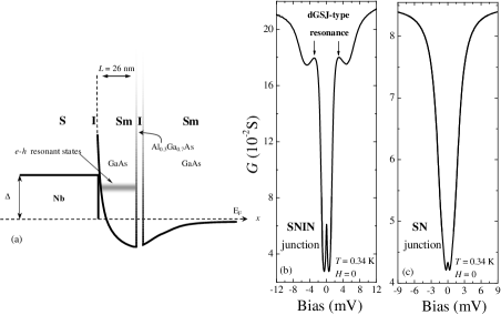
One particularly interesting case is that of a single scatterer represented by an insulating barrier (I) inserted in the structure during growth in the normal region. This configuration can give rise to controlled interference effects. Among these, one of the most intriguing is represented by de Gennes-Saint-James (dGSJ) resonances dgsj in SNIN systems where the N interlayer is characterized by a constant pair potential. The case of a null pair potential is especially relevant to the present case. Multiple reflections off the superconductive gap (i.e. Andreev reflections) and off the insulating barrier (i.e. normal reflections) may give rise to quasi-bound states dgsj ; rb that manifest themselves as conductance resonances. Transport resonances linked to similar multilayer configuration were observed experimentally in all-metal structures row ; wong ; tess , thus providing elegant evidence of quasi-particle coherent dynamics in SN systems. A qualitative sketch of the energy-band diagram of our SNIN engineered structure is depicted in Fig. 4(a).
In Fig. 4 are shown the measured differential conductance bias () for the resonant structure (SNIN engineered junction, (b)) and for the reference junction (SN structure, (c)) at K. Comparison of the two characteristics clearly shows the presence of a marked subgap conductance peak in the SNIN, resonant device. The resonance is superimposed to the typical Andreev-dominated subgap conductance. The symmetry of conductance and the ZBCP peculiar to RT further demonstrate the effectiveness of the employed fabrication protocol.

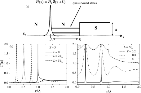
Quantitative determination of the resonant transport properties in such a system is not trivial as it can be inferred by inspecting Fig. 4(a) and considering the diffusive nature of the normal regions. dGSJ-enhancement, however, is an intrinsically ballistic phenomenon so that its essential features can be captured with relative ease. One study particularly relevant for this system was performed in Ref. rb . In the context of ballistic transport a one-dimensional SNIN structure (see Fig. 5(a)) was studied as a function of the N interlayer thickness and it was demonstrated that resonances (i.e., quasi-bound states) can occur in the subgap conductance spectrum for suitable geometric conditions. The insulating barrier was simulated by a -like potential . Customarily the barrier strength is described by the dimensionless coefficient , where is the electron Fermi velocity btk , and in the following we shall make use of it to characterize our system. The key-results of the analysis are: (i) the number of resonances increases for larger thickness of the metallic interlayer and is virtually independent of ; (ii) the energy-width of such resonances decreases for increasing . All this is better highlighted in Fig. 5(b) and 5(c). Figure 5(b) shows the calculated total transmission coefficient , where and are the energy-dependent Andreev and normal reflection transmission probabilities for the whole SNIN structure obtained through the solution of the Bogoliubov-de Gennes equations, at for and for some values of the N interlayer thickness expressed in units of the superconducting coherence length, . In these simulations we used, as an example, parameters typical for metals, i.e., the Fermi energy meV, the quasi-particle mass equal to the free electron mass and meV. From this choice follows that Å. The subgap resonances reach a transmission value due to resonant Andreev reflection at the SN interface. Increasing the N interlayer thickness allows the formation of more quasi-bound states, like in ordinary normal resonant tunneling. When the barrier is located at the SN interface we recover the expected Blonder-Tinkham-Klapwijk result btk for an opaque junction. In Fig. 5(c) is shown the calculated at for some values of barrier strength and for fixed . The other parameters of the simulations are the same as in Fig. 5(b). Increasing makes the resonances much more sharp: indeed it is possible to demonstrate rb that the energy width of the resonance, , is of the order of ; therefore, incresing the barrier strength, decreases the resonance energy width up to a monochromatic or fully-bound state in the limit of infinite barrier. The one-dimensional differential conductance at temperature can be expressed as btk
| (1) |
where , is the incoming particle energy and is the equilibrium Fermi distribution function. This model is rather idealized, but is a useful tool to grasp the essential features of our system such as number and position of resonances. We confined our calculation to the one-dimensional case in light of the results by S. Chaudhuri and P. F. Bagwell cb , that showed the insensitivity to dimensionality of the essential properties of transport resonances. These are determined by the inspection of the behavior. In order to apply it we must first determine parameters such as barrier strength, electron density and mean free path. Also, any quantitative comparison with experiment requires us to estimate the sample series resistance, which influences the experimental energy position of the resonance peak. The above parameters can be obtained from an analysis of the RT-driven ZBCP and from Hall measurements.
We performed Hall measurements at 1.5 K and obtained carrier density cm-3 and mobility cm2/V s. These data allow us to estimate the thermal coherence length m, where cm2/s is the diffusion constant, and the electron mean free path nm. compares favorably with the geometrical constraints of the structure (as a matter of fact nm ) and further supports our ballistic analysis. The ZBCP can be described following the analysis of Refs. marmor ; ben1 and described in Section III. At 0.34 K, m and in our junctions we calculate V. Comparison with the experimental value V in Fig. 6(a) (see solid line), allowed us to estimate the series resistance contribution to the measured conductivity. This rather large effect stems mainly from the AlGaAs barrier and the sample back-contact resistance.

Following Eq. 1 we calculated the conductance for the nominal N-thickness value ( nm) and , as appropriate for the AlGaAs barrier. It is indeed straightforward to determine , taking into account the Al0.3Ga0.7As/GaAs discontinuity, Fermi energy and barrier thickness. We emphasize, however, that the essential features such as the number and energy position of the dGSJ resonances are virtually independent of Z and are controlled instead by the value of . Our calculations yield a single conductance peak at energies corresponding to about . By including the above-determined series resistance contribution, the resonance peak is positioned at about mV (see Fig. 6(a), dotted line, calculated at K). The corresponding experimental value is about 3 mV (solid line in Fig. 6(a)), but the observed energy difference is well within the uncertainty resulting from the determination of the series resistance. The results of our model calculations strongly support our interpretation of the experimental structure in terms of dGSJ resonant transport. Previous results on all-metal films generally showed more complex structures resulting from several dGSJ peaks, consistent with the wider N-regions employed and the larger Fermi wave-vector values characteristic of metallic systems. Our calculations show that for our material system configurations presenting more than one peak (i.e., more quasi-bound states) are not experimentally accessible. Indeed, they show that a second peak occurs for N-region thickness exceeding 120 nm. This length unfavorably compares with the available quasi-particle coherence length particularly in light of the known four-traversal requirement for dGSJ quasi-bound state formation wolf .
Ordinary resonant tunneling in the normal double-barrier potential schematically shown in Fig. 4(a) cannot explain the observed subgap structure. This is indicated by the symmetry in the experimental data for positive and negative bias and is further proven by the temperature and magnetic field dependence of the differential conductance. Figure 6 shows a set of s measured in the 0.34-1.55 K range for the ZBCP, (b), and for the resonance peak, (c). Both effects show a strong dependence on temperature and at K are totally suppressed. This temperature value is within the range where RT suppression is expected kast ; giaz2 ; post ; sanq . At higher temperatures, the conductance in the resonance region resembles that one of the reference SN junction of Fig. 4(c). Notably, the ZBCP and the resonance peak disappear at the same temperature, hence indicating the coherent nature of the observed effect.

Further confirmation of the nature of the resonance peak can be gained observing its dependence from the magnetic field. Figure 7 shows at K for several values of the magnetic field applied in the plane of the junction for the ZBCP, (a), and for the resonance peak, (b). The measurements confirm the known sensitivity of ZBCP to the magnetic field marmor ; ben1 , and clearly indicate that the dGSJ resonance is easily suppressed for critical fields of the order of 100 mT. We also investigated the perpendicular field configuration (see Fig. 8) for the ZBCP, (a), and for the resonance peak, (b), and also in this case the resonance and the ZBCP displayed a similar dependence. Such behavior is fully consistent with dGSJ-related origin but is not compatible with a normal resonant tunneling description of the data capasso . Moreover, in the perpendicular configuration, the differential conductance spectra show a behavior similar to that one reported for the SN reference junctions in Fig. 3(b), i.e., the appearance of fluxons in the mixed state of Nb.
V Concluding remarks
In conclusion, we have reported on reflectionless tunneling-dominated transport in Nb contacts on GaAs (i.e., in SN reference junctions) and presented an effective and reproducible fabrication technique. The observed regime was studied as a function of temperature and magnetic field. Data were analyzed within the random-matrix theory of phase-coherent Andreev reflection and the impact of junction nonuniformity on reflectionless tunneling was underlined. The fabrication technique presented is compatible with the most widespread MBE systems and can be easily exploited for the implementation of novel hybrid SmS mesoscopic systems by tailoring the band-gap profile of the AlGaAs/GaAs heterostructures on which the Nb film is deposited and patterned. This was indeed developed in the SNIN engineered junctions, where we experimentally observed de Gennes-Saint-James resonant states in Nb/GaAs/AlGaAs/GaAs hybrid microstructures. In these junctions the electric transport was studied as a function of temperature and magnetic field and was successfully described within the ballistic model of Riedel and Bagwell rb . To the best of our knowledge this result represents the first demonstration of de Gennes-Saint-James resonant transport in SmS hybrid structures and was made possible by the fabrication procedure adopted in this work. The present results confirms that the Nb/GaAs/AlGaAs system is a good candidate for the implementation of complex mesoscopic structures that can take advantage of the mature AlGaAs nanofabrication technology. Such structures may represent ideal prototype systems for the study of coherent transport and the implementation of novel hybrid devices.
The experimental results reported in this paper highlight some interesting issues. The first one is related to the technique that we have adopted and refers in particular to the high reproducibility of the structures and to their large homogeneity on the lateral scale. Indeed, both in Nb/GaAs and Nb/GaAs/AlGaAs/GaAs structures the behavior was consistently the same for all the measured junctions. This is intrinsic, we believe, to the Sm surface treatment before the contact with the superconductor. The accurate lattice reconstruction achieved after the substrate annealing yields highly controlled surface conditions, avoiding those problems encountered in treating semiconductors with other methods, i.e., typically with wet or dry etching. Furthermore we would like to stress that this is a fairly simple technique. Even the choice of metals to be deposited on the semiconductor substrate is in principle extremely wide and allows to test several superconductor combinations. The drawback of this method resides in the fact that it can not be employed in those situation where the semiconducting active layer is underneath the surface. The exploitation of high-mobility semiconductor heterostructures is thus precluded.
Another important point is related to the GaAs system that proved to be a good choice for the realization of hybrid devices. Junctions showed good interface transmissivity of the order of and in principle it should be possible to engineer the GaAs doping profile in order to further enhance the interface transparency. This represents an interesting issue in order to establish an optimized protocol for interface transparency in hybrid structures fabricated with such material. The combination with AlGaAs revealed the effectiveness of tailoring the structure band profile in order to explore phase-coherent effects. The flexibility offered by the GaAs/AlGaAs system seems indeed ideally suited to design more elaborate heterostructures to probe the effect of the superconducting state. In light of these results it seems natural to reckon the possibility of extending this technique to MBE-grown InAs and In0.77Ga0.23As layers, where the lack of the Schottky barrier together with low values of the effective mass as compared to GaAs could in principle allow more easily the implementation of hybrid structures in the ballistic transport regime.
VI Acknowledgment
The authors acknowledge the financial support of INFM under the PAIS project EISS (Eterostrutture Ibride Semiconduttore-Superconduttore).
References
- (1) A. F. Andreev, Zh. Eksp. Teor. Fiz. 46, 1823 (1964).
- (2) S. De Franceschi, F. Giazotto, F. Beltram, L. Sorba, M. Lazzarino, and A. Franciosi, Appl. Phys. Lett. 73, 3890 (1998).
- (3) G. E. Blonder and M. Tinkham, Phys. Rev. B 27, 112 (1983).
- (4) C. Nguyen, H. Kroemer, and E. L. Hu, Appl. Phys. Lett. 65, 103 (1994).
- (5) T. Akazaki, J. Nitta, and H. Takayanagi, Appl. Phys. Lett. 59, 2037 (1991).
- (6) S. Lachenmann, A. Kastalsky, A. Foerster, D. Uhlisch, K. Neurohr, and Th. Schäpers, J. Appl. Phys. 83, 8077 (1998).
- (7) A. Kastalsky, A. W. Kleinsasser, L. H. Greene, R. Bhat, F. P. Milliken, and J. P. Harbison, Phys. Rev. Lett. 67, 3026 (1991).
- (8) R. Taboryski, T. Clausen, J. Bindslev Hansen, J. L. Skov, J. Kutchinsky, C.B. Sørensen, and P. E. Lindelof, Appl. Phys. Lett. 69, 656 (1996).
- (9) J. R. Gao, J. P. Heida, B. J. van Wees, S. Bakker, and T. M. Klapwijk, Appl. Phys. Lett. 63, 334 (1993).
- (10) A. M. Marsh and D. A. Williams, J. Vac. Sci. Technol. A 14, 2577 (1996).
- (11) F. Giazotto, M. Cecchini, P. Pingue, F. Beltram, M. Lazzarino, D. Orani, S. Rubini, and A. Franciosi, Appl. Phys. Lett. 78, 1772 (2001).
- (12) F. Giazotto, P. Pingue, F. Beltram, M. Lazzarino, D. Orani, S. Rubini, and A. Franciosi, Phys. Rev. Lett. 87, 216808 (2001).
- (13) D. K. Schroder, Semiconductor Material and Device Characterization (Wiley Interscience, New York, 1990).
- (14) J. Kutchinsky, R. Taboryski, T. Clausen, C. B. Sørensen, A. Kristensen, P. E. Lindelof, J. Bindslev Hansen, C. Schelde Jacobsen, and J. L. Skov, Phys. Rev. Lett. 78, 931 (1997).
- (15) I. K. Marmorkos, C. W. J. Beenakker, and R. A. Jalabert, Phys. Rev. B 48, 2811 (1993).
- (16) C. W. J. Beenakker, B. Rejaei, and J. A. Melsen, Phys. Rev. Lett. 72, 2470 (1994).
- (17) B. J. van Wees, P. de Vries, P. H. C. Magnée, and T. M. Klapwijk, Phys. Rev. Lett. 69, 510 (1992).
- (18) A. Badolato, F. Giazotto, M. Lazzarino, P. Pingue, F. Beltram, C. Lucheroni, and R. Fazio, Phys. Rev. B 62, 9831 (2000).
- (19) K. Neurohr, A. A. Golubov, Th. Klocke, J. Kaufmann, Th. Schäpers, J. Appenzeller, D. Uhlisch, A. V. Ustinov, M. Hollfelder, H. Lüth, and A. I. Braginski, Phys. Rev. B 54, 17018 (1996).
- (20) C. W. J. Beenakker, Rev. Mod. Phys. 69, 731 (1997).
- (21) D. Quirion, F. Lefloch, and M. Sanquer, J. Low Temp. Phys. 120, 361 (2000).
- (22) W. M. van Huffelen, T. M. Klapwijk, D.R. Heslinga, M. J. Boer, and N. van der Post, Phys. Rev. B 47, 5170 (1993).
- (23) P. G. de Gennes and D. Saint-James, Phys. Lett. 4, 151 (1963).
- (24) R. A. Riedel and P. F. Bagwell, Phys. Rev. B 48, 15198 (1993).
- (25) J. M. Rowell, Phys. Rev. Lett. 30, 167 (1973).
- (26) L. Wong, S. Shih, and W. J. Tomasch, Phys. Rev. B 23, 5575 (1981).
- (27) S. H. Tessmer, D. J. V. Harlingen, and J. W. Lyding, Phys. Rev. Lett. 70, 3135 (1993).
- (28) G. E. Blonder, M. Tinkham, and T. M. Klapwijk, Phys. Rev. B 25, 4515 (1982).
- (29) S. Chaudhuri and P. F. Bagwell, Phys. Rev. B 51, 16936 (1995).
- (30) See, for example, E. L. Wolf, Principles of Electron Tunneling Spectroscopy (Oxford University Press, New York, 1985), p. 193.
- (31) P. H. C. Magnée, N. van der Post, P. H. M. Kooistra, B. J. van Wees, and T. M. Klapwijk, Phys. Rev. B 50, 4594 (1994).
- (32) W. Poirier, D. Mailly, and M. Sanquer, Phys. Rev. Lett. 79, 2105 (1997).
- (33) F. Capasso, Physics of Quantum Electron Devices (Springer-Verlag, Berlin, 1990).