Core-level spectroscopy of Si/SiO2 quantum wells: evidence for confined states
Abstract
We present an experimental and theoretical study of the conduction states of crystalline Si films confined within amorphous SiO2 barriers, using the Si- core-level excitations. The spectral peaks near the conduction band minimum are compared with the bulk silicon spectrum. In the Si quantum wells, it is found that the conduction band minimum and the low-lying peaks undergo a blue shift while all higher peaks remain unshifted. The experimental results are supported by calculations using recent first-principles structural models for Si/SiO2 superlattices. The experimental results suggest that all conduction states up to a given conduction band offset become confined and blue-shifted while those at higher energies are not confined and undergo no shift. These results provide unambiguous evidence that the visible-light emitting properties of Si/SiO2 structures depend strongly on electron confinement effects.
pacs:
78.66.Jg, 68.65.Fg, 71.23.CqThe discovery of luminescence in porous silicon set off strong efforts towards the fabrication of Si-based light-emitting nanostructures. Thus, Si-nanocrystallites, wires, layers, as well as Si/Ge superlattices have been studied in this context.mrs97 A study of luminescence in Si/SiO2 quantum wells (QWs) was reported by Lu et al., where evidence for quantum confinement was presented.llb Many studies of Si-luminescence have led to similar or quite different conclusions involving explanations in terms of surface defect centers, self-trapped excitons, siloxene derivatives and so forth.kanemistu ; mrs95 On the theory side, while several studies have established the importance of electron confinement in Si by the SiO2,pcarDBM ; pcarMRS ; garoufalis ; jap ; pcarFRM others have emphasized the role of interface statesKageshima and some even questioned the relevance of confinement in these structures containing amorphous barriers. Also, experimental studies which attempted to probe the conduction band density of states (DOS) failed to see clear evidence of electron confinement in Si/SiO2 QW structures. Meanwhile, the local-energy gap on the SiO2 side has been probed using electron energy-loss spectroscopy (EELS) by Neaton et al.neaton
We report in this Letter experimental Si- core-level spectroscopy results coupled with first-principles calculations of atomistically-detailed Si/SiO2 QW structures to demonstrate electron confinement and the resulting blue shifting. Confined states are directly relate to the width of the Si-layer, as opposed for instance to impurity states that are uncorrelated to any geometric parameter. In Si/SiO2 QWs, only states found within the energy range of an effective conduction-band offset (CBO) are expected to be confined, while band states above should remain unconfined. This scenario is analysed from both experiment and theory sides.
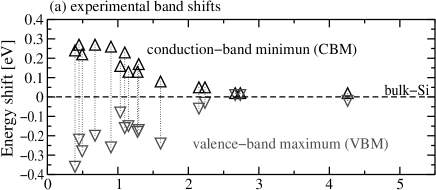
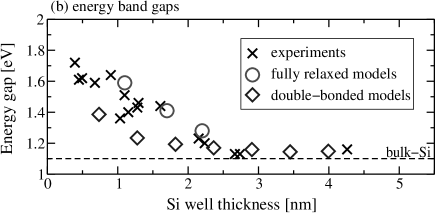
Very recently, the fabrication of crystalline SiO2/Si/SiO2 QWs have been reported by Lu and Grozea.lg The QWs having various thicknesses were examined using a synchrotron source; X-ray photoelectron spectra (XPS) as well as X-ray absorption near-edge spectra (XANES) were recorded. The valence-band maxima (VBM) and conduction-band minima (CBM) were deduced respectively from the XPS and the XANES. All data were calibrated according to an assumed null VBM for crystalline silicon (c-Si), corresponding to the limit of an infinitely thick silicon well. The results for the energy shifts of the VBM and the CBM as a function of the Si well width are summarized in Fig. 1(a). The energy gaps were obtained by summation of the reference energy gap of c-Si (1.12 eV) with the relative CBMs and VBMs. The resulting energy gaps are compiled in Fig. 1(b). The bandgaps are compared with two theoretical models obtained within the density-functional theory (DFT) and the local density approximation (LDA), where all bandgaps are raised by 0.6 eV (corresponding to the difference between the LDA and experimental bandgaps of c-Si). The theoretical energy gaps for the QWs are found to be in good agreement with the experiments.
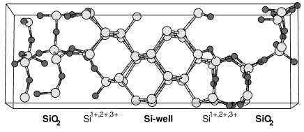
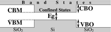
We have carried out atomistically-detailed calculations using a first-principles-based energy optimized Si/SiO2 interface model, where Si-well layers are coupled to “amorphized” SiO2 layers. The structure is based on one of the Si/SiO2/vacuum interface models of Pasquarello et al,alfredo1 extended to a SiO2/Si/SiO2 system by Tit and Dharma-wardana,jap and finally fully optimized by Carrier, Lewis, and Dharma-wardana,pcarFRM wherein can be found calculations of the electronic states, optical matrix elements and densities of states. The detailed atomic structure of the 1.1 nm QWs is shown in Fig. 2. Definitions of the VBM, CBM and the corresponding energy gap () evaluated in Fig. 1, as well as definitions of the CBO and VBO, are also schematized. The three suboxide Si atomic species (Si1+, Si2+, and Si3+) are present at the interfaces, as indicated in Fig. 2. Complete details about structural deformations from the bulk can be found in Ref. pcarFRM, .
Consider now a piece of matter which is in an initial state with total energy together with a probe photon of energy . The interaction leaves the system in a final state of energy together with an emitted photon of energy . The process involves the absorption of a photon of energy = if no free electrons are emitted in the final state. By sweeping the probe photon energy so that transitions from the core-states of Si are excited to the empty states in the conduction band of Si, the energies of the electronic states in the conduction band can be determined. The energy change includes all initial-state as well as final-state interactions and can be calculated using DFT, since the latter provides an approach to accurate total energies. On the other hand, within the Fermi Golden rule, the absorption spectrum of the probe photon is given in terms of matrix elements and joint densities of states (jDOS) obtained by a convolution of the initial and final densities of states, In our case the initial-DOS is that of the Si- core-state at the energy . This is a discrete relativistic doublet of states, and hence a sum of -functions. Thus, the jDOS is essentially proportional to the sum of pure conduction electron densities of states. The matrix element connecting the initial and final states will select only the final states which have - and -symmetries.fuggle The transition rate is thus determined, first, by:
Second, the electron binding energies of the and core-states are separated by 0.6 eV (98.8 - 98.2 eV).fuggle The final expression for the Si- core-level absorption is thus obtained by summation of shifted transitions rate :
| (1) |
The - and -DOS calculated in a straightforward way using Kohn-Sham methods will have several shortcomings: (a) The absolute position of the DOS peaks would not be correct due to the well known underevaluation of the bandgap; (b) the effect of final-state interactions would not be contained in the standard calculation of the DOS; (c) the type of photon renormalization effects arising from time-dependent response is not contained in the standard DOS evaluation.zangwill Some of these shortcomings can be overcome by using fairly simple modifications to the DOS evaluation, e.g., the Slater-transition-states (STS) method.tian ; DreizlerGross
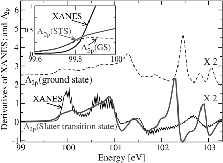
Figure 3 shows the measured XANES derivative combined with two theoretical Si- absorption derivatives, one obtained from the STS and the other from the ground states (GS), all for c-Si. Both calculations are performed within the all-electron, linearized-augmented-plane-waves (LAPW) framework.WIEN The STS calculation is set by simultaneously reducing and increasing by one-half the electronic charge of the 2 core level and the total number of valence electrons, for a Si atom in the FCC cell. This is imposed during the whole iterative process. In this way, the excess valence electron gets promoted to some conduction levels The - and -DOS’s of c-Si are then combined with their matrix elements. The latter are shown to vary slowly and monotonically as and for energies above the Fermi level, up to 8 eV. This is in contrast to the results of Buczko et al.Buczko where a constant and much lower ratio is reported.
We first observe from Fig. 3 that above the Fermi level (at 100 eV) up to 102 eV, the STS and the XANES are in very good agreement. Thus the STS is clearly an improvement on the GS calculation as expected from equi-ensemble DFT.DreizlerGross Second, the sharp peak at 102.7 eV in the XANES derivative is downshifted to 102.2 eV in the STS (as well as for the GS based calculation). One should remark that the XANES intensities get significantly damped for energies high above the threshold (due to an acute angle of the photon probe tangent to the sample), while no damping is included in the calculations. Finally, we observe that, in spite of several shifts of the energy peaks in the GS, the general aspect of the GS and STS theoretical curves resemble. However, the GS is clearly expanded in the near-edge region of the spectrum (from 99.5 to 102 eV) compared to the STS, in agreement with previous calculations (see Ref. Buczko, and reference therein); moreover, above 102.5 eV, the GS shows several features not visible in the STS. This comparison of the STS and GS theoretical approaches for c-Si is essential to the analysis that follows, applied to the Si/SiO2 QWs (solely in the GS, owing to their large size as can be appreciated from Fig. 2; and hence no STS results are available).
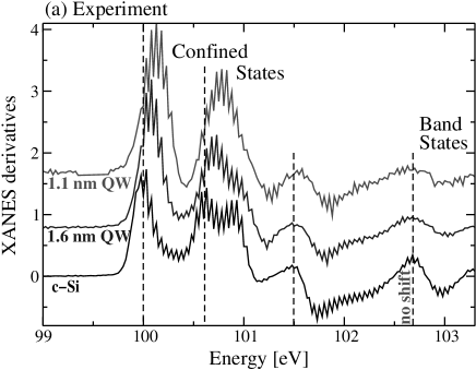
Figure 4(a) depicts the XANES derivatives of two QWs, 1.1 nm and 1.6 nm thick, as well as for c-Si. The lowest energy edges at the Si-conduction band minimum ( 100 eV) shifts to the blue as we go from c-Si to the 1.1 nm Si well. This trend continues until we reach peaks at and above 102.7 eV. The first peaks above are seen to be unshifted with respect to the c-Si peaks. This is easily explained if we assume that the Si/SiO2 interfaces are associated with a CBO of 2.7 eV. However, given the 9 eV bandgap of crystalline SiO2 and the 1.1 eV bandgap of c-Si, this leads to a VBO of about 3.95 eV, as commonly assumed.williams Thus the XANES suggests that a large reduction in the CBO has occurred.
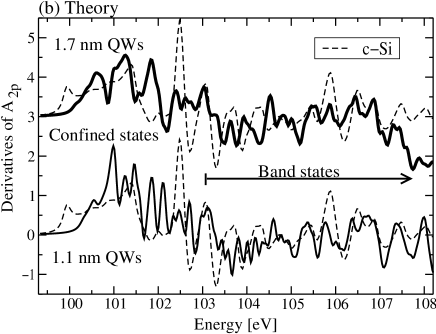
In order to evaluate the electronic properties of the confined states, a calculation of obtained from Eq. (1) has been applied to Si atoms inside two Si wells. The matrix elements are deduced from c-Si, calculated within the LAPW and the STS approaches given above, while the - and -DOS’s are evaluated in the GS, within the projector-augmented-waves (PAW) approach.VASP Thus, in this procedure, we assume that the matrix elements of Si0 atoms (i.e., Si atoms inside only the Si well) are equivalent to their counterpart in c-Si. This assumption is justified by the observed slow variation with of the two matrix elements and , as discussed before. Figure 4(b) shows the mean (lorentzian) derivatives of for Si0 atoms in the 1.1 nm and 1.7 nm Si/SiO2 QWs, as well as for c-Si. The Si- absorption of the QWs are presented for energies that correspond to the CBM region.
We first observe from Fig. 4(b) that the absorption intensities in the near-edge region, from 100 eV to 102.7 eV, for both QWs, are much higher than for c-Si (with their respective energy gaps preserved) leading to enhanced absorption propertiespcarFRM and strong confinement effects in this region. Second, a comparison of the two QWs together in the “band states” region from 103.5 eV to higher energies gives in general good agreement between each other. However, a complete correspondence between any of the QWs with c-Si only appears at energies above 105.7 eV; for instance, some features appearing in both QWs (e.g., a triplet of decreasing peaks at 105 eV) are not present in c-Si. Thus, the electronic properties of silicon in confined structures are modified high above the CBO. In the region between 102.7 eV and 105.7 eV, both QWs show rather similar features, while no complete agreement lies between any of the QWs with c-Si. This suggests a “transition domain” for the band states region where the QWs together have similar electronic properties but different from c-Si.
Thus, within the GS, two main regions are observed in the QWs, as from the XANES: one having strong confined states, and another region of band states constituted of a transition domain where their electronic properties are slightly different from c-Si and for much higher energies a region of pure c-Si band states. It is important to recall that the absorption calculations presented in Fig. 4(b) for the QWs (and c-Si) do not incorporate any approximations for the excited states, such as the STS approach used for c-Si as shown in Fig. 3; informations contained in Fig. 4(b) thus remain qualitative.
In summary, the detailed electronic structures within confined crystalline wells have been measured for the first time. The XANES data show rich electron states in these crystalline silicon wells, in dramatic contrast to featureless XANES from amorphous silicon wells.llb The data show dramatic blue shift for electron states at the band edge (i.e., the bottom of the well). The magnitude of the shift decreases as the energy levels increase and eventually there is no shift for states above 2.7 eV from CBM, as one would expect from elementary quantum mechanics for a finite-well system. On the theory side, we have built detailed atomic models for the SiO2/Si/SiO2 system. Based on such realistic models, we have developed theoretical methodologies to calculate XANES data. Ground states calculations for the theoretical QWs give a confined states region much higher in energy than in experiment, with a transition domain where electronic properties of the QWs are together alike but different from c-Si. Strong confinement has been confirmed both from experiment and the present ground-state study, that provides qualitative insights on the electronic properties, i.e., for excited states. An excited states description applied to the quantum wells, such as the Slater-transition-state theory applied here to the c-Si, would provide further accurate knowledge of the confinement effects in these Si nanostructures.
Acknowledgments – This work is supported by grants from the NSERC of Canada and the FCAR of the Province of Québec. We are indebted to the RQCHP for generous allocations of computer resources. We thank CANNON ELTRAN for providing us the SOI wafers.
References
- (1) L. T. Canham, Appl. Phys. Lett. 57, 1046 (1990); D. J. Lockwood et al., in MRS Symposia Proceedings 452, 183 (Material Research Society, Warrendale, 1997).
- (2) Z. H. Lu, D. J. Lockwood and J.-M. Baribeau, Nature, 378, 258 (1995).
- (3) Y. Kanemitsu et al., Appl. Phys. Lett. 76, 2200 (2000); V. Mulloni et al., Philos. Mag. B, 80, 705 (2000).
- (4) X. Huang et al., MRS Symposia Proceedings 358, 839 (Material Research Society, Warrendale, 1995)
- (5) P. Carrier, L. J. Lewis and M. W. C. Dharma-wardana, Phys. Rev. B, 64, 195330 (2001).
- (6) P. Carrier et al., MRS symposia proceedings 677, AA4.10 (Material Research Society, Warrendale, 2001).
- (7) C. S. Garoufalis et al., Phys. Rev. Lett. 87, 276402 (2001).
- (8) N. Tit and M. W. C. Dharma-wardana, J. App. Phys. 86, 1 (1999).
- (9) P. Carrier, L. J. Lewis and M. W. C. Dharma-wardana, Phys. Rev. B, 65, 165339 (2002).
- (10) H. Kageshima and K. Shiraishi, in Materials and Devices for Silicon-Based Optoelectronics, edited by J.E. Cunningham, S. Coffa, A. Polman, and R. Soref, Mater. Res. Soc. Symp. Proc. 486, 337 (Material Research Society, Pittsburgh, 1998).
- (11) J. B. Neaton, D. A. Muller, and N. W. Ashcroft, Phys. Rev. Lett. 85, 1298 (2000); D. A. Muller et al., Nature 399, 758 (1999).
- (12) Z.H. Lu, D. Grozea, Appl. Phys. lett. 80, 255 (2002).
- (13) A. Pasquarello, M. S. Hybertsen, and R. Car. Appl. Phys. lett. 68, 625 (1996); Phys. Rev. Lett. 74, 1024 (1995).
- (14) J.C. Fuggle, in Unoccupied Electronic States, edited by J.C. Fuggle and J.E. Inglesfield, Topics in Applied Physics Vol. 69 (Springer-Verlag, Berlin, 1992).
- (15) A. Zangwill and P. Soven, Phys. Rev. A 21, 1561 (1980); see also F. Perrot and M. W. C. Dharma-wardana, Phys. Rev. Lett. 71, 797 (1993) where photon renormalization effects are shown to be small for deep lying core-states.
- (16) Z. Tian et al., Phys. Rev. B 55, 5376 (1997); J. F. Janak, Phys. Rev. B 18, 7165 (1978).
- (17) R. M. Dreizler, E. K. U. Gross, Density Functional Theory, An approach to the Quantum Many-Body Problem (Springer-Verlag, Berlin, 1990).
- (18) P. Blaha et al., Comput. Phys. Commun. 59, 399 (1990).
- (19) R. Buczko, G. Duscher, S. J. Pennycook, S. T. Pantelides, Phys. Rev. Lett. 85, 2168 (2000).
- (20) G. Kresse and J. Furthmüller, Comput. Mater. Sci. 6, 15 (1996).
- (21) R. Williams, J. Vac. Sci. Technology, 14, 1106 (1977); A. Demkov, O. F. Sankey, Phys. Rev. Lett. 83, 2038 (1999) propose a VBO of 4.35 eV.