Conductance of a Quantum Point Contact in the presence of a Scanning Probe Microscope Tip
Quantum point contacts (QPCs) formed in two-dimensional electron gases (2DEGs) have attracted significant attention for the past two decades.[1, 2] Since the discovery of the conductance quantization in these structures,[1] QPCs have been widely used in a variety of investigations, including transport through quantum dots, the quantum Hall effect, magnetic focusing, and the Aharonov-Bohm effect. [2] Also, with the rapid development on scanning probe microscope (SPM) techniques, it is possible to image current directly to study many remarkable phenomena, including quantum corrals,[3] electron flow through nanostructures,[4] charge distribution and photoactivity of dopant atoms,[5] and spectra of metallic nanoclusters.[6] Since the QPC plays such an important role in mesoscopic devices, it is an ideal system to be studied by the SPM techniques.
Very recently, Topinka et al. have directly imaged the electron flow from the QPC by scanning a negatively charged SPM tip above the surface of the device and measuring the position-dependent conductance simultaneously.[7, 8] In the experiment, as the width of the QPC increases, the conductance increases in quantized steps of , as was also reported in other experiments.[1] Besides, several new and interesting features were observed. Widening of the angular structure of electron flow has been clearly seen as the QPC channel becomes wider. Another feature of their images is the appearance of fringes spaced by half the Fermi wavelength transverse to the electron flow, which clearly shows the character of coherent quantum interference. The above fringes are thermally smeared out by increasing the effective electron temperature. Moreover, when the tip is placed such that it interrupts the flow from particular modes of the QPC, a reduction can be observed in the conductance of those channels, while other channels are not affected.[7] On the other hand, it is also found that, in contrary to intuitions, the electron flow from the point contact forms narrow branching strands instead of smoothly spreading fans.[8]
Using the recursive Green’s function technique, in this paper, we study theoretically a mesoscopic structure similar to the experimental one.[7, 8] Our numerical results are able to explain the experimental finding in Refs.7,8. Therefore, the recursive Green’s function technique seems to be a suitable method to study the coherent electron conductance in such a mesoscopic system.
We consider a negatively charged SPM tip capacitively coupled to the 2DEG where the QPC is formed. The effect of SPM tip is that, the conductance will decrease if the tip is positioned over regions with high electron flow from the QPC, while it will be less modified if the tip is at low electron flow regions. The electron flow can be imaged by scanning the tip over the two-dimensional surface. Two contributions to the potential in the 2DEG region should be taken into account. One is from the negatively charged gates that define the QPC, which we model with the Büttiker saddle-point potential with as the gate voltage, as the electron effective mass and as the strength of the lateral confinement. This potential is a practical candidate to reproduce the quantized conductance of a QPC.[9] The other is a Lorentzian type potential induced by the SPM tip,[10] which we approximate as a delta function in the present work : , where denotes the position of the tip, and is a negative constant. It is worth noting that the numerical results obtained with the simple delta potential are consistent the experimental results.[7, 8]
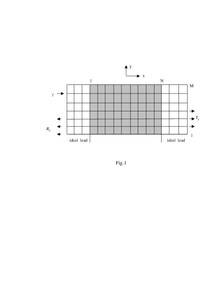
We use a 2D square lattice model to describe the QPC system. The sites of the lattice are denoted as with to be set equal to unit, and . The lattice may be divided into three regions, as shown in Fig.1. The shadowed central zone is a mesoscopic structure with a Büttiker saddle-point potential and scanned by a SPM tip. Both sides of the structure are assumed to be connected with semi-infinite ideal leads to simplify scattering boundary conditions. The one-electron tight-binding Hamiltonian of the system takes the form [11]
| (1) | |||||
| (2) |
where and is a orthonormal set in the lattice sites . The on-site energy in the central zone is given by . Then the Hamiltonian for this region reads
| (3) |
where denotes the set of ket vectors belonging to the -th cell, and
The Hamiltonians for the two ideal leads have the same form as Eq.(3), but with different summing regions ( at the left lead and at the right lead) and .
Using the recursive Green’s function technique, the transmission amplitude for the incident channel and outgoing channel is found to be[11, 12]
| (4) |
where with , with
The set of vectors are the duals of the set , defined by where
with as the transposition of matrix. is the retarded Green’s function for the scattering region between two ideal leads, which can be obtained by a set of recursion formulas in a matrix form, [12, 13]
| (5) | |||||
| (6) |
by iteration starting form , where , and .
At finite temperature , the conductance through a 2D mesoscopic structure is given by the Landauer-Büttiker formula[14]
| (7) |
where is the transmission coefficient, and is the Fermi-Dirac distribution with as the Fermi energy and as the Boltzmann constant. Obviously, at zero temperature Eq.(7) reduces to .
The above formulas are valid under the assumption that the voltage across the device is low. High voltage will raise the energies of electrons flowing from the QPC. Thus, as shown by van Wees et al., [15] the conductance at a finite voltage has a similar behavior to that with a finite temperature effect, and is given by
| (8) |
In the following we calculate numerically the conductance of a QPC system with the size and . We set and the lattice constant as the units of energy and length, respectively. In order to obtain well-pronounced quantized plateaus with the Büttiker saddle-point potential, we choose , , and .
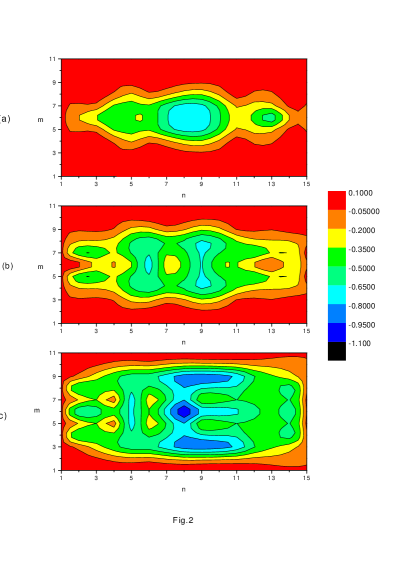
At zero temperature and low voltage limit, images of electron flow from the 2D surface of the QPC are plotted in Fig.2. The gate voltage is chosen to ensure Fig.2(a) - (c) correspond to the first, the second and the third conductance plateau of the QPC, respectively. It is seen clearly that a new electron flow pattern appears when a higher mode is opened (then the conductance of the QPC rises to another plateau) by decreasing the gate voltage. This feature agrees with the result reported in Ref.7: electronic wavefunctions inside the QPC have maxima when QPC has conductance modes. Note that the images do not turn into smoothly spreading fans as the electrons flow across the QPC from the left to the right. Instead, they form branching strands which are relatively narrower. In fact, even the width of the sample decreases to in the calculation, the images change little (not shown here). It is not surprising that strands are formed in our model since the electrons are laterally confined. On the other hand, a similar but also striking phenomenon is reported in Ref.8, where the strands were found in regions far away from the point contact . So we can see that the electron path has a rare probability to pass through the edge regions of the sample, and thus the impurity density and the boundary scattering in these regions are less relevant to the conducting property of the QPC. Moreover, the fringe structures due to the alternating constructive and destructive interference of electrons are evident in Fig.2, though the distribution is not so homogeneous when compared with the experiments.[7] This inhomogeneity induced from the varieties of electron wavelength inside the QPC is the main difference between the structure of fringe inside and outside QPC. It is worth pointing out that the fringes directly demonstrate the coherent character of electron flow in QPC.
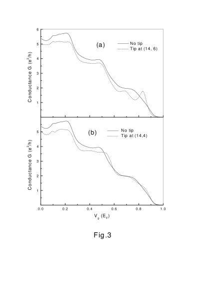
Meanwhile, we also note that the angular structures in these electron flow patterns are quite different from each other, especially for the first and second modes. For the first mode, the pattern contains one branch only, while there are two branches for the second mode. So there are some regions in the 2D surface where the distribution of electrons at one mode make no contribution to the other mode. As reported in experiments,[7] when the SPM tip is placed over these regions, only the flow from particular channels of the QPC are changed, while other channels are not affected. This phenomenon is clearly manifested in Fig.3, where the quantized curves of the QPC with or without the SPM tip are plotted. From the comparison between the behaviors of the solid line and the dash line in Fig.3(a), we can see that when the tip is placed at the central axis of the QPC where the electrons from the first mode travel through, the heights of all plateaus are reduced. But the height difference between each pair of neighboring plateaus remains to be , except for that between the first plateaus and the -axis. In Fig.3(b), the SPM tip is positioned off the central axis. According to Fig.2(a) and (b), we can learn that this position corresponds to in the first mode, and it only affects the second mode. Thus in Fig.3(b) it is shown that the first conductance plateau is almost unchanged, and the second and other higher plateaus are lowered. Again, the height difference between the second and the third plateaus still remains to be .
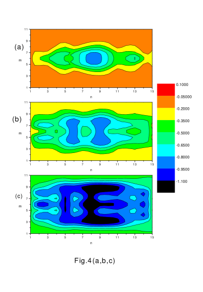
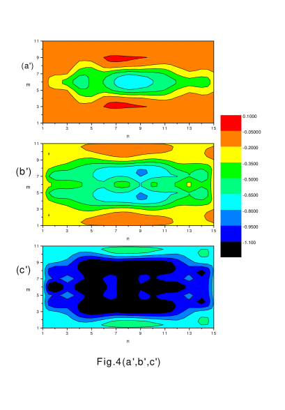
The electron flows under the finite voltages across the QPC are imaged in Fig.4, where are at a low voltage and are at a high voltage . Comparing it with Fig.2, we see that the pattern still remains the same in each mode, but the values of is no longer so severely fluctuated when the voltage is raised. A more important characteristic of voltage effect is that fringe structure would gradually disappear as the voltage rises. Actually, we find that the three conductance modes gradually merge into one conductance mode, which implies that the quantized plateaus also disappear as the voltage is increased. The origin of the fringes is the coherent quantum interference.[7] Since the fringes are less perceptible as the fluctuation of becomes pacified, it is manifested that the consequence of using effectively hotter electrons is to smear out the coherence among electrons. The above properties are similar for elevating temperature as the physical effects of temperature and voltage are the same here.[15] Clearly, the voltage effect addressed here is in qualitative agreement with the experimental observation.[7]
In conclusion, we have calculated the conductance of a QPC in the presence of the SPM tip by the recursive Green’s function technique. The numerical results are able to explain the experimental results in Refs.7,8.
This work was supported in part by the RGC grant of Hong Kong under Grant No. HKU7118/00P. G. P. H. was supported in part by the NSF of Guangdong Province (Contract No.011151) and the Foundation of Zhongshan University Advanced Research Centre (Contract No.02P2). Z. D. W. also thanks support in part from the Texas Center for Superconductivity at the University of Houston. S. L. Z. was supported in part by the NSF of Guangdong under Grant No. 021088.
REFERENCES
- [1] B. J. van Wees, H. van Houten, C. W. J. Beenakker, J. G. Williamson, L. P. Kouwenhoven, D. van der Marel, and C. T. Foxon, Phys. Rev. Lett. 60, 848 (1988); D. A. Wharam, T. J. Thornton, R. Newbury, M. Pepper, H. Ahmed, J. E. F. Frost, D. G. Hasko, D. C. Peacock, D. A. Ritchie, and G. A. C. Jones, J. Phys. C 21, L209 (1988).
- [2] C. W. J. Beenakker and H. van Houten, Solid State Phys. 44, 1 (1991).
- [3] M. F. Crommie, C. P. Lutz, and D. M. Eigler, Science 262, 218 (1993); E. J. Heller, M. F. Crommie, C. P. Lutz, and D. M. Eigler, Nature 369, 464 (1994); H. C. Manoharan, C. P. Lutz, and D. M. Eigler, Nature 403, 512 (2000).
- [4] M. A. Eriksson, R. G. Beck, M. Topinka, J. A. Katine, R. M. Westervelt, K. L. Campman, and A. C. Gossard, Appl. Phys. Lett. 69, 671 (1996); R. Crook, C. G. Smith, C. H. W. Barnes, M. Y. Simmons, and D. A. Ritchie, J. Phys. Cond. Matt. 12, L167 (2000).
- [5] M. J. Yoo, T. A. Fulton, H. F. Hess, R. L. Willett, L. N. Dunkleberger, R. J. Chichester, L. N. Pfeiffer, and K. W. West, Science 276, 579 (1997).
- [6] L. Gurevich, L. Canali, and L. P. Kouwenhoven, Appl. Phys. Lett. 76, 384 (2000).
- [7] M. A. Topinka, B. J. LeRoy, S. E. J. Shaw, E. J. Heller, R. M. Westervelt, K. D. Maranowski, and A. C. Gossard, Science 289, 2323 (2000).
- [8] M. A. Topinka, B. J. LeRoy, R. M. Westervelt, S. E. J. Shaw, R. Fleischmann, E. J. Heller, K. D. Maranowski, and A. C. Gossard, Nature 410, 183 (2001).
- [9] M. Büttiker, Phys. Rev. B 41, 7906 (1990).
- [10] M. A. Eriksson, R. G. Beck, M. A. Topinka, J. A. Katine, R. M. Westervelt, K. L. Campman, and A. C. Gossard, Superlattices Microstruct. 20, 435 (1996).
- [11] S. L. Zhu, Z. D. Wang, and L. Hu, J. Appl. Phys.91, 6545 (2002).
- [12] T. Ando, Phys. Rev. B 44, 8017 (1991); S. Sanvito, C. J. Lambert, J. H. Jefferson, and A. M. Bratkovsky, ibid. 59, 11936 (1999).
- [13] P. A. Lee and D. S. Fisher, Phys. Rev. Lett. 47, 882 (1981); L. Schweitzer, B. Kramer, and A. MacKinnon, J. Phys. C 17, 4111 (1984); A. MacKinnon, Z. Phys. B 59, 385 (1985).
- [14] R. Landauer, IBM J. Res. Dev. 1, 223 (1957); M. Büttiker, Phys. Rev. Lett. 57, 1761 (1986).
- [15] B. J. van Wees, L. P. Kouwenhoven, E. M. M. Willems, C. J. P. M. Harmans, J. E. Mooij, H. van Houten, C. W. J. Beenakker, J. G. Williamson, and C. T. Foxon, Phys. Rev. B 43, 12431 (1991).