Even-odd effects in magnetoresistance of ferromagnetic domain walls
Abstract
Difference in density of states for the spin’s majority and minority bands in a ferromagnet changes the electrostatic potential along the domains, introducing the discontinuities of the potential at domain boundaries. The value of discontinuity oscillates with number of domains. Discontinuity depends on the positions of domain walls, their motion or collapse of domain walls in applied magnetic field. Large values of magnetoresistance are explained in terms of spin-accumulation. We suggest a new type of domain walls in nanowires of itinerant ferromagnets, in which the magnetization vector changes without rotation. Absence of transverse magnetization components allows considerable spin accumulation assuming the spin relaxation length, , is large enough.
pacs:
73.50.-h, 73.61.-r, 75.60.Ch, 75.70.PaAs it was demonstrated first in Johnson ; Sohn , spin accumulation effects in the presence of a current flowing between ferromagnetic and normal metals may result in a considerable contribution to a contact’s resistivity. This phenomenon is the key element for the GMR devices with the CPP (current perpendicular to the plane) geometry. The CPP-GMR effect has been studied theoretically for the spin-valve systems for a simple triple layer and multi-layered structures in the pioneering work Valet . The subsequent experiments (see e.g. Pratt ; Piraux ; Dubois ) were in excellent agreement with the predictions made in Valet concerning the dependence of the resistivity on the width of magnetic and non-magnetic components and the role played by spin-relaxation mechanisms. Most recently it was discovered that nanocontacts Garcia and domain walls in magnetic nanowires Ebels possess significant magnetoresistance.
Realization of different experimental configurations allows determination of parameters present in the expressions in Ref. [Valet, ] such as the values of resistivity for each of the GMR components and what is most important the spin relaxation length, , characterizing the width of a non-equilibrium distribution of spins near the contacts Piraux ; Dubois .
The formulas in Ref. [Valet, ], however, have been derived in assumption that while the conductivities of the majority and minority spins are different, the corresponding densities of states (DOS), , remain equal. This assumption is not realistic. In the presentation below we address this issue to demonstrate that taking difference in the DOS into account, the changes in the expressions for the distribution of the electrostatic potential lead to some new observable effects. In Ref. [Garcia, ; Ebels, ] it was speculated that the pronounced GMR effects are caused by the significant role of spin accumulation. We suggest, as we believe, for the first time, that large magnetoresistance observed in Ref. [Ebels, ] is due to the non-rotational character of the domain walls Zhirnov which are possible in itinerant ferromagnets Dzero .
Following Valet , we re-write the expression for the current , ( - the electrostatic potential, the index, , stands for the majority and minority spins correspondingly), into the form:
| (1) |
where
| (2) |
is a non-equilibrium (in the presence of a total current, ) electrochemical potential for each spin component, and the relation is used in (1, 2).
The equations for the current components:
| (3) |
together with (2) and the electro-neutrality condition:
| (4) |
present the complete system of equations for each side of an interface (in (3) is a spin relaxation time).
To simplify the analysis, we at first assume the ballistic regime for the interface, i.e. the width of the corresponding domain wall is small (contributions due to the spin scattering inside the barrier will be discussed at the end of the paper). Correspondingly and are taken continuous at the boundary.
Subtracting one of Eqs. (3) from another and making use of (5), one obtains the equation for the distribution of in the “bulk” on each side of the contact:
| (6) |
where
| (7) |
Equation (6) coincides in its form with Eq. (14) from Ref. [Valet, ]. For our purposes it is convenient to re-write (6) as:
| (6’) |
Equation (6) applies now everywhere in the sample. In (6’), stands for the Dirac delta-function at the boundary () (equation ((6’) is valid when the boundary between the domains is abrupt). While is continuous, has a jump at the interface:
| (8) |
The jump can be expressed in terms of the total current, . To do so, we write down the expressions for , spin current , to obtain with the help of (4,5):
| (9) |
We specify that on the left from the domain wall spins up belong to the majority band. Magnetization changes sign across the wall and so does the band’s occupation so that one has to interchange between in (9). Since the currents are continuous, for the jump of electrochemical potential gradient, , we get:
| (10) |
For a multilayer system, Eq. (6’) reads:
| (11) |
It is also assumed below that the width of the very left and very right banks are larger then . The solution of (11) is a superposition of solutions for a single domain wall:
| (12) |
We consider first the behavior of the electrostatic potential, , close to a single domain wall. With the help of Eq. (5) one can write:
| (13) |
Making use of continuity of the electrochemical potential at the boundary, one immediately sees from (13) that potential is discontinuous with the jump at the th domain wall:
| (14) |
The spatial distribution of can be found by integrating the first equation (9) along each side of the domains:
| (15) |
The total potential drop across an isolated single domain wall in the chosen geometry is the sum of two terms:
| (16) |
(the second term in (16) comes about from the currents distribution (12) on the distances of the order of on the two sides of the wall). In the following notations
one obtains:
| (17) |
i.e. drop out from the total magnetoresistance. Equations (16-17) coincide with the results obtained in Valet . The differences in the DOS for the minority and majority spins lead to an appearance of the discontinuities (14) and changes in the dependence of the electrostatic potential (see (15)) along the domains.
To make a numerical estimate for the total potential drop we will use the data from Ref. [Ebels, ] obtained for Co nanowires: nm, . The typical values of are of the order of Piraux ; Dubois , while is of the order of Janak . After substituting these values in (17), the resistance drop per unit area is , or for the geometry used in Ebels . The value of the potential drop at domain boundary is approximately the same as the value of the total potential drop in (16):
| (17’) |
We would like to emphasize, that the ratio in (17’) may also be negative.
As an example, let us consider in some more details, the drop of the potential, , across the very left domain for a system of walls (we also take ). From (12) and (14) we have
| (18) |
where
| (18’) |
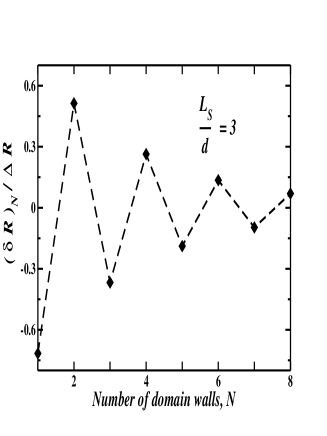
For the walls the value of shows an interesting “even-odd” effect:
| (19) |
Below in Fig. 1 we plot as a function of number of the domain walls. The “even-odd” effect is well-pronounced at , where is a size of domain.
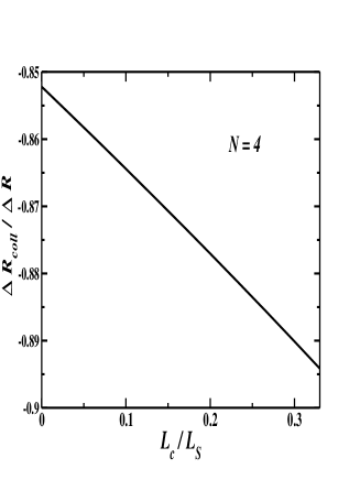
Another interesting feature is that changes in Eq. (18) could follow a motion of a single domain wall, say at , through its contribution into (18’), or even a collapse of a domain caused by the applied magnetic field (such a collapse has been experimentally seen in Ref. [Ebels, ]). In order to explicitly demonstrate this effect, we first introduce the following notations:
The result of our calculations of as a function of the distance between two neighboring domains is plotted in Fig. 2. Experimentally, the motion of a domain wall can be detected by the STM technique.
Now we would like to briefly discuss the change in our results in case when one takes the finite width of the domain wall into account. In particular, we consider the importance of depolarizing effects in the Bloch or Neél type of domain wall for the results above. Since the width of the wall is usually much smaller then the spin diffusion length, , the arguments that lead us to results given by (14-16) still hold. The only modification would come from the change in the boundary conditions for the spin current.
Electrons going through the Bloch or Neél domain wall loose part of its polarization because the transverse component of magnetization inside the wall creates a torque which causes spin’s re-orientation. Obviously this process will reduce the spin accumulation. If is the width of a domain wall, spins of electrons traveling through the wall are rotated in the transverse component of the exchange field, , in the wall by an angle :
| (20) |
From (20) one obtains:
| (21) |
with given by:
| (21’) |
and after some algebra with help of (5):
| (22) |
Taking into account (22), the expression for the jump of at the interface is:
| (23) |
As a result, the expression for the potential drop across an isolated domain wall acquires the form:
| (24) |
To estimate the value of , we first re-write the second expression in (24) as:
| (25) |
where is a mean free path and is the Fermi velocity. Using the data, provided in Ebels , we have: eV, nm, , cm/s, cm/s. Thus our estimates provide , which according to (23) significantly reduces the spin accumulation effect. This result can also be explained slightly differently: from (20) we estimate the depolarization angle , i.e. at crossing the Bloch or Neél type of domain wall the electronic spins would adiabatically follow magnetization. To reconcile the above estimates with the significant magnetoresistance experimentally observed in Ref. [Piraux, ; Ebels, ], we suggest that the domain walls in these experiments were neither of the Bloch nor Neél type. Instead, in itinerant ferromagnets another type of domain walls, “linear walls”, is realized Dzero . In a linear wall the direction of magnetization does not change, while its absolute value goes through zero inside the wall. Theoretically, “linear” domain walls were considered in Zhirnov for local spin ferromagnetic systems at temperatures close to critical temperature .
To summarize, we have shown that taking into account difference in the density of states between the minority and majority spin bands drastically changes the distribution of the electrostatic potential along the domains. The discontinuities of the potential across each domain wall are of particular interest. The jumps in the values of potential can be measured directly by the STM technique. Jumps possess such characteristic features as the “even-odd” effects counting the total number of domain walls in magnetic nanowire in the presence of an external magnetic field. Our results can be directly extended to the GMR structures consisting of F/N layers which were studied theoretically in Valet in the approximation of equal density of states of majority and minority bands. To ascribe large values of magnetoresistance observed in Piraux ; Ebels to spin accumulation effects, it was also necessary to suggest that in nanowires made of itinerant ferromagnets the domain walls are of a linear type in which magnetization changes without creating a perpendicular component that would revert spins of polarized electrons.
The work of M.D. was supported by DARPA through the Naval Research Laboratory Grant No. N00173-00-1-6005, L.P.G. by the NHMFL through the NSF cooperative agreement DMR-9527035 and the State of Florida, A.K.Z. through the NISVP Supplement to the core NHMFL Grant No. 5024-599-22 and the State of Florida, and K. A. Z. by the RFBR grant No. 02-02-17389.
References
- (1) M. Johnson and R. B. Silsbee, Phys. Rev. B 35, 4959 (1987); Phys. Rev. Lett. 60, 377 (1988).
- (2) P. C. von Sohn, H. van Kempen and P. Wyder, Phys. Rev. Lett. 58, 2271 (1987).
- (3) T. Valet and A. Fert, Phys. Rev. B 48, 7099 (1993).
- (4) W. P. Pratt, Jr., S. F. Lee, J. M. Saurenbach, and J. Bass, Phys. Rev. Lett. 66, 3060 (1991); S. F. Lee, W. P. Pratt, Jr., R. Loloee, P. A. Schroeder, and J. Brass, Phys. Rev. B 46, 548 (1992).
- (5) L. Piraux, S. Dubois, and A. Fert, J. of Magn. Magn. Mater. 159, L287 (1996).
- (6) S. Dubois, L. Piraux, J. M. George, K. Ounadjela, J. L. Duvail, A. Fert, Phys. Rev. B 60, 477 (1999).
- (7) N. Garcia, M. Munoz, and Y.-W. Zhao, Phys. Rev. Lett. 83, 2030 (1999); G. Tatara, Y.-W. Zhao, M. Munoz, and N. Garcia, Phys. Rev. Lett. 83, 2030 (1999); N. Garcia, M. Munoz, and Y.-W. Zhao, Appl. Phys. Lett. 76, 2586 (2000); N. Garcia, M. Munoz, G. G. Qian, H. Rohrer, I. G. Saveliev, and Y.-W. Zhao, Appl. Phys. Lett., 79, 4550 (2001).
- (8) U. Ebels, A. Radulescu, Y. Henry, L. Piraux, and K. Ounadjela, Phys. Rev. Lett. 84, 983 (2000).
- (9) V. A. Zhirnov, Sov. Phys. JETP 8, 822 (1959).
- (10) M. Dzero, L. P. Gor’kov and A. K. Zvezdin, unpublished.
- (11) E. I. Rashba, Phys. Rev. B 62, R16267 (2000).
- (12) V. L. Moruzzi, J. F. Janak and A. R. Williams, Calculated electronic properties of metals (New York : Pergamon Press, 1978).