Spin-polarized bipolar transport and its applications
Abstract
In spin-polarized bipolar transport both electrons and holes in doped semiconductors contribute to spin-charge coupling. The current conversion between the minority (as referred to carriers and not spin) and majority carriers leads to novel spintronic schemes if nonequilibrium spin is present. Most striking phenomena occur in inhomogeneously doped magnetic p-n junctions, where the presence of nonequilibrium spin at the depletion layer leads to the spin-voltaic effect: electric current flows without external bias, powered only by spin. The spin-voltaic effect manifests itself in giant magnetoresistance of magnetic p-n junctions, where the relative change of the magnitude of electric current upon reversing magnetic field can be more than 1000%. The paper reviews nonmagnetic and magnetic spin-polarized p-n junctions, formulates the essentials of spin-polarized bipolar transport as carrier recombination and spin relaxation limited drift and diffusion, and discusses specific device schemes of spin-polarized solar cells and magnetic diodes.
I Introduction
Semiconductor spintronics dassarma01 ; dassarma00a ; dassarma00b is a growing field where the fundamentals of spin-polarized transport and spin relaxation processes optical84 ; fabian99 in homogeneous and inhomogeneous semiconductors are being developed, and novel electronic device schemes based on active control of spin in semiconductor heterostructures are being proposed. Semiconductor spintronic devices now include various spin field-effect transistors, spin valves and spin detectors, and spin bipolar diodes and transistors dassarma01 . The potential of semiconductor spintronics is underscored by the discoveries of novel magnetic semiconductors (some of which are reported to remain ferromagnetic even at room temperature CdMnGeP ; reed02 ; hebard02 ; matsumoto01 ; cho02 ), which can be successfully incorporated with nonmagnetic semiconductors to extend the functionality of traditional semiconductor devices. Furthermore, it has been demonstrated that the ferromagnetism in semiconductors can be controlled both optically koshihara97 ; oiwa02 and electrically ohno00 ; park02 .
While some of the interest, stimulated by possible applications, to actively manipulate spin in semiconductors has only emerged in recent years, theoretical understanding for spin manipulation in electronic materials has been steadily accumulated over the last several decades dassarma00a ; optical84 ; fabian99 ; rashba02a ; zutic02 . Often the concepts currently applied to spintronics schemes involving semiconductors have been initially investigated in other materials systems or in simpler nonmagnetic homogeneous semiconductors. Crucial for spintronics is spin-charge coupling, where spin degrees of freedom influence transport of charges and, vice versa, where spin transport depends on nonequilibrium charges. Spin-charge coupling appears at a microscopic level, where individual electron dynamics depends on the electron spin orientation, the fact usually expressed by the spin-orbit term in the Hamiltonian. Another form of spin-charge coupling occurs in statistical ensembles of electrons where spin and charge are coupled because electrons carry both spin and charge and because the Pauli principle limits the occupation of the states to single spins. As a result, the transport properties of an electronic system are greatly influenced by spin polarization, since electrons taking part in transport will have different densities of states, Fermi velocities, scattering times, etc., for different spin orientations. The microscopic nature of spin-charge coupling is exemplified by the Rashba effect rashba60 ; rashba84 occurring typically in GaAs-like semiconductor interfaces, where the spin-orbit interaction and thus the spin-charge coupling in the system can be effectively controlled by electric fields (say from a biasing gate nitta97 ; miller02 ). Additional studies have examined the Rashba spin-orbit interaction in many other systems ( for example, near the interfaces with superconductors gorkov01 and in interacting quantum wires hausler01 ). The statistical spin-charge coupling was initially suggested by Aronov and Pikus aronov76a ; aronov76b . They were the first to realize that electrical spin injection is possible: the charge current flowing from a ferromagnetic electrode can give rise to nonequilibrium spin in the connected paramagnetic metal or semiconductor. The reverse process, that of generating charge current (or emf in an open circuit) by nonequilibrium spin, was first described by Silsbee silsbee80 , and later demonstrated experimentally and developed further theoretically by Johnson and Silsbee johnson85 ; johnson87 , to serve the purpose of detecting the amount of the injected spin by electrical means. The Silsbee-Johnson spin-charge coupling was realized as the phenomenon where the presence of nonequilibrium (ensemble) spin influences charge properties of the interfacial system. In particular, the Silsbee-Johnson spin-charge coupling states that an emf appears across the interface of a magnetic and a paramagnetic metal, if nonequilibrium magnetization is maintained (by external spin injection, for example) in the paramagnetic metal.
Rashba’s ideas significantly influenced spintronics by giving rise to the concept of the spin field-effect transistor of Datta and Das datta90 . This proposal stimulated an extensive body of work on spintronic devices and ballistic and mesoscopic spin-polarized transport. Our own work on spin-polarized bipolar transport–what we call bipolar spintronics–drew from the ideas of Silsbee and Johnson on spin-charge coupling as a statistical notion. The motivation we had in mind was to examine the effect of both electrons and holes on spin-polarized transport in inhomogeneous semiconductors and to propose simple device structures dassarma00c ; zutic01a ; zutic01b ; zutic02a ; zutic02b ; fabian02a ; fabian02b where possible applications of bipolar spintronics can be studied. One of the devices we consider, the magnetic p-n junction zutic02a ; fabian02a , is a generalization of the Silsbee-Jonhson coupling to nondegenerate semiconductor interfaces (essentially depletion regions). When the minority region of a p-n junction is magnetic (that is, it has a significant, on the level of thermal energy, equilibrium spin band splitting of the minority carriers) and the corresponding majority region is nonmagnetic, electric current will flow through the junction if nonequilibrium spin is maintained at the depletion layer in the nonmagnetic majority side. This is the spin-voltaic effect zutic02a ; zutic02b ; fabian02a in magnetic p-n junctions, which is also manifest as a giant magnetoresistance of the junction when forward bias is applied.
In this paper we first review the Silsbee-Johnson concept of spin-charge coupling, then introduce the equations for spin-polarized bipolar transport in inhomogeneous magnetic semiconductors, and finally discuss two specific bipolar spintronic schemes: spin-polarized p-n junctions zutic01a ; zutic01b and magnetic diodes zutic02a ; zutic02b ; fabian02a .
II Silsbee-Johnson spin-charge coupling
As recently emphasized by Rashba, spin emf is a specific manifestation of the general principle that macroscopic (dissipative) currents flow in nonequilibrium situations rashba02a ; rashba02b ; landau36 . Since both spin and charge are carried by electrons, nonequilibrium spin can give rise not only to spin current, but to electric current (or emf, properly called spin emf, in an open circuit) as well. This is a purely statistical property of the charge and spin carriers, not of the microscopic dynamics of electrons according to a spin-dependent Hamiltonian (of the Rashba type, for example). Spin-dependent dynamics manifests itself here only on the macroscopic level in limiting the amount of the accumulated nonequlibrium spin and in the conversion of the spin energy into thermal energy in the process of spin relaxation.
In the Silsbee-Johnson effect the ferromagnetic and paramagnetic degenerate electron systems (metals or degenerate semiconductors) form an electrical and spin contact. Generating nonequilibrium spin in the paramagnetic system makes, say, spin up electrons flowing into the ferromagnet, and, vice versa, spin down electrons (if the spin down subband is not fully occupied) flow in the opposite direction. These two currents are not in balance, due to the unequal conductances of the two spin species in the ferromagnet, resulting in a charge current. If the two systems were paramagnetic metals, no charge current would flow, since equal currents would flow in both directions. The only flowing current (this is a nonequilibrium situation after all) would be spin current. The Silsbee-Johnson effect is also a spin-valve effect, since the electric current direction can be reversed by reversing either the nonequilbrium spin in the paramagnet or the equilibrium magnetization of the ferromagnet.
Silsbee and Johnson succeeded to measure the induced open circuit spin emf of the order of pico volts, which is equivalent to measuring one spin per 1011 johnson85 . To obtain the value of spin emf, consider for simplicity the ferromagnet to be an ideal Stoner ferromagnet with only the minority (say, spin up) spin electrons participating in current conduction (the majority spin subband is fully occupied). Maintaining nonequilbrium spin in the paramagnet means maintaining a difference in the chemical potentials between the two spins. This difference leads to charge current across the interface, proportional to the difference between the chemical potential of spin up electrons in the paramagnet and in the ferromagnet. In an open circuit, the current does not flow and the chemical potential for spin up electrons will be constant across the interface, which will be achieved by the build up of the spin emf . The spin emf is simply the difference between the chemical potentials when current flows. This difference can be written for degenerate statistics as , where is the Bohr magneton, is the nonequilbrium magnetization in the paramagnet, and is the density of states in the paramagnet at the Fermi level. Considering that for degenerate electron gas paramagnetic susceptibility is , the spin emf becomes
| (1) |
For a realistic ferromagnet in which both spin states are conducting the right hand side of Eq. 1 is multiplied by a suitably defined spin polarization johnson87 .
The described spin-charge coupling can be used to detect nonequilibrium spins at magnetic-paramagnetic interfaces, and, when combined with spin injection, inquire about spin diffusion lengths in the paramagnet without the need to apply magnetic field. We will show below that a nonlinear (in bias voltage) analogue of the spin-charge coupling in degenerate systems exists in nondegenerate semiconductors, where the role of the interface is played by the depletion layer sandwiched between a magnetic and nonmagnetic semiconductor forming a p-n junction.
III Spin-polarized bipolar transport
Spin-polarized bipolar transport refers to transport in doped semiconductors where both electrons and holes contribute to charge and spin currents. Usefulness of the concept of spin-polarized bipolar transport is demonstrated in microelectronic device schemes, most prominently in novel magnetic p-n junctions which are formed by inhomogeneously doped–both with donors and acceptors, and with magnetic impurities inducing large carrier -factors–semiconductors. Traditional p-n junctions tiwari92 are the basis for all electronic (and part of optical) information technology, since they form both bipolar junction transistors and unipolar MOSFETs, as well as photodiodes, light emitting diodes, and diode lasers. It is a great challenge for spintronics to take advantage of the existing semiconductor technology and extend its capabilities, for example, to build on-single-chip computer logic processors and nonvolatile random access memory. We believe that magnetic diodes may prove fundamental devices also in semiconductor spintronics.
Nonequilibrium spin can be injected into semiconductors and then be transported by drift and diffusion throughout the sample. The transport is limited by spin relaxation. If, in addition, both electrons and holes form the current, the transport is further limited by carrier (electron and hole) recombination. This bipolar transport is particularly important in p-n junctions, where charge current depends on how fast electrons and holes recombine (in other words, on how fast the minority, say electron current, is converted to the majority hole current in the region of the junction). The presence of nonequilibrium spin either enhances the current by helping building up the minority carrier density, or inhibits the current by reducing the minority carrier density. We will demonstrate this response of charges to nonequilbrium spin in magnetic p-n junctions in a subsequent chapter.
The general drift-diffusion equations for bipolar carrier and spin transport in inhomogeneous magnetic semiconductors were first written in Ref. zutic02a . Several limiting cases of these equations, for a homogeneous magnetic martin02 and nonmagnetic yu02 semiconductor, have been subsequently investigated. For illustration, consider only electrons to be spin polarized, leaving holes spin unpolarized. Denote as , , and electron, hole, and (electron) spin densities. Electron () and spin () currents are fabian02a
| (2) | |||||
| (3) |
where is electron diffusivity, is the electric potential (from the applied bias and built-up internal charges), and is the equilibrium spin splitting of the conduction band (arising from the large electron factor and applied magnetic field). The first terms on the right hand sides are the electric drift, the second terms are the magnetic drift, while the last terms represent electron and spin diffusion arising from nonuniform electron and spin densities. In this paper we write the potentials in the units of , where is the Boltzmann constant, is temperature, and is proton charge. The drift and diffusion of electrons and spin are limited by electron-hole recombination processes, as well as by spin relaxation processes. This limitation can be expressed by continuity relations, which in a steady state read
| (4) | |||||
| (5) |
where is the constant of the electron-hole recombination rate and is the spin relaxation time. The subscript zero denotes the equilibrium values (when no external bias is applied and spin is in equilibrium). Spin polarization is denoted here as . Together with Poisson’s equation relating the built-up charge density to electric potential , the above equations for carrier and spin drift and diffusion, and carrier recombination and spin relaxation fully describe the steady state density and current profiles of carriers and spins in inhomogeneous magnetic semiconductors. The equations cannot be solved exactly analytically, and one must resort to numerical methods for general cases. We have solved the equations for a few cases of interest, including spin-polarized p-n junctions zutic01a , spin-polarized solar cells zutic01b , and magnetic p-n junctions zutic02a . We have also succeeded in solving the equations analytically for the general case of spin-polarized magnetic p-n junctions at low biases fabian02a , the regime in which most devices based on p-n junctions operate. In the subsequent sections we describe several elementary bipolar spintronic devices, and illustrate their properties using mainly the results of our numerical calculations.
IV Bipolar spintronic devices
The most fundamental bipolar spintronic device is a spin-polarized magnetic p-n junction. Such a device in equilibrium has, in general inhomogeneous, spin splitting of the carrier bands, and the nonequilibrium spin can be externally injected. The equilibrium spin splitting can be caused, for example, by doping the junction inhomogeneously with magnetic impurities and placing the junction in a magnetic field. Another possibility is to use ferromagnetic semiconductors (ferromagnetic at a specific donor or acceptor doping density to achieve inhomogeneity). Since spin-polarized magnetic p-n junctions form quite a general group of devices, it is useful to consider particular cases of interest. Below we consider spin-polarized nonmagnetic p-n junctions, which are just ordinary p-n junctions but with nonequilibrium spin added (by illumination of circularly polarized light or external spin injection, for example) and spin-polarized magnetic p-n junctions in which one of the regions, or , is magnetic in equilibrium, but the equilibrium spin splitting is constant throughout this specific region. Fascinating phenomena occur also in p-n junctions in which the magnetic region itself is magnetically inhomogeneous (as described in Ref. fabian02a ), and where magnetic drift plays active role in determining charge transport. We will not discuss such devices here, due to their added complexity. What all the spin-polarized (magnetic and nonmagnetic p-n junctions) have in common is the interplay between charges and spins, and the fundamental concept which we have formulated, namely the spin injection through the depletion layer. Bipolar spintronics is useful only so far as spins can be injected from the majority region into the minority one (and vice versa) through the depletion layer. We will illustrate below how this concept of spin injection is realized in the two cases of nonmagnetic and magnetic spin-polarized p-n junctions.
IV.1 Spin-polarized p-n junction
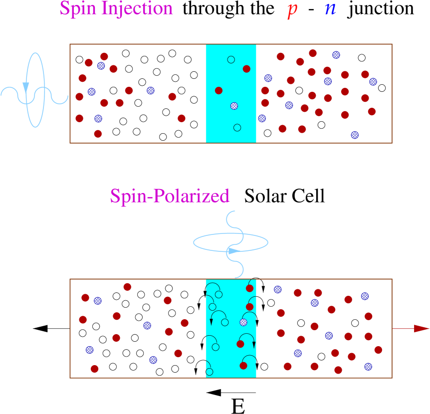
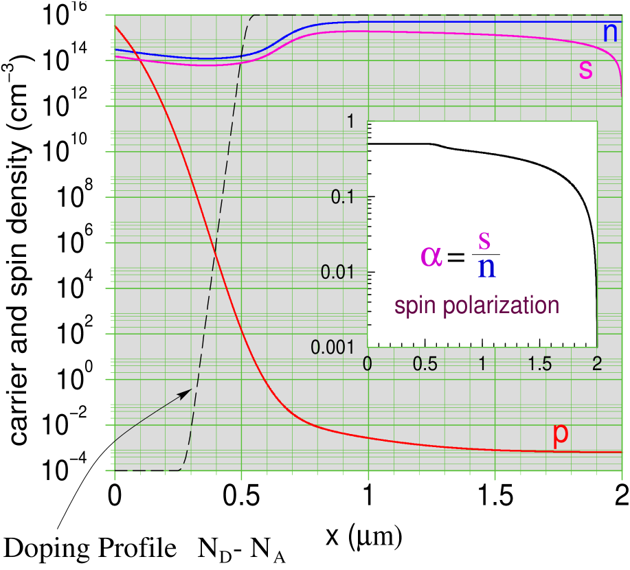
A spin-polarized p-n junction is a p-n junction where spin-polarized current flows as a result of external spin excitation. We have considered the cases where nonequilibrium spin is created by shining circularly polarized light on one of the ends of the junction (see Fig. 1). In all our simulations we keep only electrons spin polarized and the externally injected (what we call source) spin was implemented as a boundary condition in the drift-diffusion equations. The fundamental question of whether source spin can be further transported across the depletion layer has positive answer. Both spin injection from the region to the region, and vice versa, from the region to the region are very effective.
If source spin appears in the region, this means that the minority electrons are spin polarized. Since both carrier (here synonymous for electron) and spin densities are out of equilibrium if light illuminates the sample in the region, the electrons carrying spin diffuse towards the depletion layer where they are swept by the large built-in field to the side, where they form the majority carriers. In the region the spin can further diffuse away from the depletion layer, or relax by processes. If the light illumination creates electrons per second per unit volume, with spin polarization , the spins at the depletion layer in the side appear with the rate of roughly . Considering that all the electrons (and thus spins) arriving at the depletion layer are swept to the side, this rate must equal, in a steady state, the rate of spin relaxation and spin diffusion in the side. A typical scale for these rates is . As a result, the nonequilibrium injected spin in the majority region is (more complete considerations better theory give , where is the effective spin relaxation time in the minority region). This is normally larger than the spin in the minority region itself, an effect we called spin amplification zutic01a . The descriptive name for the effect is spin pumping of the majority carriers by the minority channel, since it is analogous to spin pumping by circularly polarized light of majority carriers in semiconductors. Our numerical calculation demonstrating the effect is given in Fig. 2.
One application of a spin-polarized p-n junction is a spin-polarized solar cell (Fig. 1). If circularly polarized light illuminates the junction close to the depletion layer, nonequilibrium charges and spins can arrive in the layer and be powered by the equilibrium built-in electric field to form a spin-polarized current. This could be useful in generating spin-polarized currents zutic01b . Another use of spin pumping by the minority carriers is in significantly extending the effective spin diffusion length (again the effect of the built-in field) and in making it possible to control, by an applied reverse bias to the junction, the amount of the injected nonequilibrium spin zutic01a . The width of a depletion layer changes with the applied bias, which changes the amount of spin arriving in the side at the depletion layer. This significantly affects the amount of injected spin. We called this effect the spin capacitance effect zutic01a , since it is an analogue of the voltage to charge relation in capacitors.
The question of injected spin across the depletion layer from the majority (here ) side to the minority one is of equal importance, since diodes operating under forward biases would be able to carry the spin information from one lead to the other across the junction. Injecting spin from the majority to the minority side is also important for potential applications of spintronics in bipolar junction transistors zutic01a ; fabian02b , where two p-n junctions would operate back-to-back and both spin injection regimes would be needed for injecting spin all the way through the transistor, as well as for amplifying the spin-polarized current from the emitter to the collector. Our numerical calculationszutic01a ; zutic01b demonstrate that spin injection by the majority carriers is very effective. Spin polarization does not change significantly upon entering the region. As we have shown analytically fabian02a , the nonequilibrium spin polarization is actually uniform across the depletion layer. So whatever spin-polarization arrives at the depletion layer from the region, it must appear across in the side.
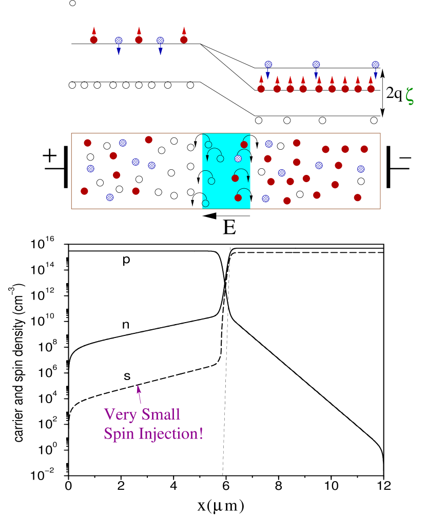
IV.2 Magnetic diode
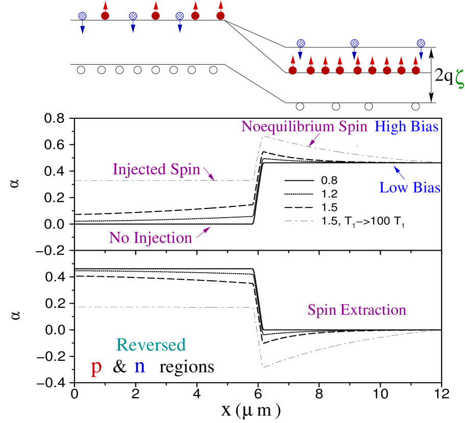
A magnetic p-n junction would typically contain magnetic impurities to amplify its magnetic response. An applied magnetic field would lead to significant (on the scale of the thermal energy) spin splitting furdyna88 ; dietl94 ; fiederling99 ; jonker00 of carrier bands in such a junction. Here we consider a particular case where only one of the regions is magnetic, and the equilbrium spin splitting is constant within the region (that is, the spin splitting varies only in the transition region of the junction). The fundamental question of spin injection through the depletion layer is more complicated than in nonmagnetic junctions. It would be natural to expect that if, say, the region is magnetic and the junction is under forward bias, spin injection would occur since spin-polarized electrons from the region carry the spin into the minority side, similarly to what happens in ferromagnet-paramagnetic metal spin injection. We have demonstrated rather that spin injection in magnetic p-n junctions can occur only at large biases, beyond the usual region of interest for devices. At small biases, where the junctions show their typical exponential rectification I-V characteristics, spin injection is not possible. The reason is as follows. Let there be more spin up than spin down electrons in the region. The current electrons with a particular spin orientation across the depletion layer depends on the number of electrons available for transport and on the barrier height for thermal transport across the junction’s depletion layer. This barrier is higher for spin up than for spin down electrons, exactly compensating for the greater density of the former. As a result, spin current will not flow across the depletion layer and spin will not be injected. This is the consequence of the fact that at low biases the depletion layer can be considered to be (quasi)equilibrium, and only nonequilibrium spin can be injected through the depletion layer. Once the bias is increased, nonequilibrium spin accumulates already in the magnetic region, and the spin is then injected thought the depletion layer to the minority nonmagnetic side. The corresponding numerical calculation is shown in Fig. 4, where we also discuss the opposite case of spin injection from the minority magnetic side. There spin injection appears rather as spin extraction, and contains the same physics as large bias spin injection from the magnetic majority side.
Magnetic p-n junctions are potentially useful for their nonlinear spin-charge coupling. This coupling appears at low biases if nonequilibrium source spin is introduced into the junction. Spin polarization can then be injected through the depletion layer without difficulties. In addition, the nonequilibrium spin significantly affects charge transport across the junctions. Consider the case when the minority region is magnetic and the majority region is nonmagnetic, but a source spin is externally injected into the region (either by illuminating with a circularly polarized light or by a third-terminal spin injection zutic02b ; fabian02a ). As the source spin diffuses towards the depletion layer, it will come into contact with the equilibrium magnetization of the minority region. The nonequilibrium spin perturbs the balance between the generation and recombination currents across the depletion layer, leading to a net charge current. Remarkably, this current flows even if the external biasing battery is switched off. The current is powered by nonequilbrium spin, in analogy with the current across the ferromagnet-paramagnetic metal in the Silsbee-Johnson effect. And similarly to the Silsbee-Johnson effect, the charge current can change its direction by reversing the external magnetic field (that is, by reversing the equilibrium polarization of the magnetic side) or by reversing the orientation of the source spin. This is the spin-voltaic and the spin valve effect of magnetic p-n junctions introduced in Refs. zutic02a ; zutic02b ; fabian02a .
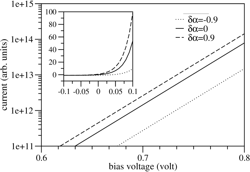
More important is the effect of source spin on the I-V characteristic of the junction. By applying forward bias, the spin-charge coupling is magnified (exponentially in ideal junction diodes), leading to large giant magnetoresistance of the junction. We illustrate here this effect with the help of our analytic formula derived using the model introduced in Ref. fabian02b . The charge current in the junction with nonequilibrium source spin polarization in the side of the depletion layer and the equilibrium spin polarization on the side of the junction is
| (6) |
where is the generation current of the diode (a material constant, which, however, depends on magnetic field through the dependence of the equilibrium minority carrier density on it). In Fig. 5 we plot the I-V characteristic (with the current rescaled by ) for a magnetic p-n junction with , and the source spin polarizations , 0, and 0.9. Giant magnetoresistance is manifest by changes in the magnitude of the current upon changing the relative sign of and . In the example shown, the change in the current is one order of magnitude, which is a relative change of 1000%. Giant magnetoresistance would further increase with the magnitudes of and . We do not see fundamental reasons why such large magnetoresistance changes (to be compared to typically 30-50% in metal-based giant magnetoresistance and 25% in all-semiconductor structures schmidt01 ) would not be reproduced.
V Conclusions
We have reviewed the fundamental concepts of spin-charge coupling and of bipolar spintronics. We have formulated spin-polarized bipolar transport in inhomogeneously doped magnetic semiconductors as carrier (electron and hole) recombination and spin relaxation limited drift and diffusion, and discussed the solutions–both numerical and analytic–of these equations for particular cases. The first important case was a nonmagnetic but spin-polarized p-n junction, with spin introduced into the minority region. We have discussed how the spin can be injected through the depletion layer leading to spin pumping in the majority side and to spin amplification. The other device scheme where our equations can be solved to predict the charge response to nonequilibrium spin is magnetic diode, in which magnetic doping in one of the two regions is inhomogeneous. The diode can serve to inject spin from the magnetic majority region only at large biases where nonequilibrium spin develops first in the magnetic region. The most striking phenomena of the spin-voltaic effects, spin-valve effects, and giant magnetoresistance appear in magnetic p-n junctions if nonequilibrium spin is externally injected to the majority nonmagnetic region, and the minority region is magnetic. The predicted phenomena (particularly giant magnetoresistance with possibly more than 1000% efficiency) should be technologically useful for sensing magnetic fields and, more generally, for injecting, manipulating, and storing spin in spintronic devices.
This work was supported by DARPA, the US ONR, and the NSF-ECS.
References
- (1) S. Das Sarma, J. Fabian, X. Hu, and I. Žutić, Solid State Commun. 119, 207 (2001).
- (2) S. Das Sarma, J. Fabian, X. Hu, and I. Žutić, IEEE Transaction on Magnetics 36, 2821 (2000).
- (3) S. Das Sarma, J. Fabian, X. Hu, and I. Žutić, Superlattice Microst. 27, 289 (2000).
- (4) F. Meier and B. P. Zakharchenya (eds), Optical Orientation (North-Holland, New York 1984).
- (5) J. Fabian and S. Das Sarma, J. Vac. Sci. Technol. B 17, 1780 (1999).
- (6) G. A. Medvedkin, T. Ishibashi, T. Nishi, K. Hayata, Y. Hasegawa, and K. Sato, Jpn. J. Appl. Phys. 39, L949 (2000).
- (7) M. L. Reed, N. A. El-Masry, H. H. Stadelmaier, Appl. Phys. Lett. 79, 3473 (2001).
- (8) N. Theodoropoulou, A. F. Hebard, M. E. Overberg, C. R. Abernathy, S. J. Pearton, S. N. G. Chu, and R. G. Wilson, cond-mat/0201492.
- (9) Y. Matsumoto, M. Murakami, T. Shono, T. Hasegawa, T. Fukumura, M. Kawasaki, P. Ahmet, T. Chikyow, S. Koshihara, and H. Koinuma, Science 291, 854 (2001).
- (10) S. Cho, S. Choi, G.-B. Cha, S. C. Hong, Y. Kim, Y.-J. Zhao, A. J. Freeman, J. B. Ketterson, B. J. Kim, Y. C. Kim, and B.-C. Choi, Phys. Rev. Lett. 88, 257203 (2002).
- (11) S. Koshihara, A. Oiwa, M. Hirasawa, S. Katsumoto, Y. Iye, S. Urano, H. Takagi, and H. Munekata, Phys. Rev. Lett. 78, 4617 (1997).
- (12) A. Oiwa, Y. Mitsumori, R. Moriya, T. Supinski, and H. Munekata, Phys. Rev. Lett. 88, 137202 (2002).
- (13) H. Ohno, D. Chiba, F. Matsukura, T. Omiya, E. Abe, T. Dietl, Y. Ohno, and K. Ohtani, Nature 408, 944 (2000).
- (14) Y. D. Park, A. T. Hanbicki, S. C. Erwin, C. S. Hellberg, J. M. Sullivan, J. E. Mattson, T. F. Ambrose, A. Wilson, G. Spanos, and B. T. Jonker, Science 295, 651 (2002).
- (15) E. I. Rashba, J. Supercond. 15, 13 (2002).
- (16) I. Žutić, J. Supercond. 15, 5 (2002).
- (17) E. I. Rashba, Sov. Phys. Solid State 2, 1109 (1960).
- (18) Y. A. Bychkov and E. I. Rashba, J. Phys. C 17, 6039 (1984).
- (19) J. Nitta, T. Akazaki, H. Takayanagi, and T. Enoki, Phys. Rev. Lett. 78, 1335 (1997).
- (20) J. B. Miller, D. H. Zumbühl, C. M. Marcus, Y. B. Lyanda-Geller, D. Goldhaber-Gordon, K. Campman, and A. C. Gossard, cond-mat/0206375.
- (21) L. P. Gor’kov and E. I. Rashba, Phys. Rev. Lett. 87, 037004 (2001).
- (22) W. Häusler, Phys. Rev. B 63, 121310 (2001).
- (23) A. G. Aronov and G. E. Pikus, Sov. Phys. Semicond. 10, 698 (1976).
- (24) A. G. Aronov, JETP Lett. 24, 32 (1976).
- (25) R. H. Silsbee, Bull. Magn. Reson. 2, 284 (1980).
- (26) M. Johnson and R. H. Silsbee, Phys. Rev. Lett. 55, 1790 (1985).
- (27) M. Johnson and R. H. Silsbee, Phys. Rev. B 35, 4959 (1987).
- (28) S. Datta and B. Das, Appl. Phys. Lett. 56 665 (1990).
- (29) S. Das Sarma, J. Fabian, X. Hu, and I. Žutić, 58th DRC (Device Research Conference) Conference Digest, p. 95-8 (IEEE, Piscataway, 2000); cond-mat/0006369.
- (30) I. Žutić, J. Fabian, and S. Das Sarma, Phys. Rev. B 64, 121201 (2001).
- (31) I. Žutić, J. Fabian, and S. Das Sarma, Appl. Phys. Lett. 79, 1558 (2001).
- (32) I. Žutić, J. Fabian, and S. Das Sarma, Phys. Rev. Lett. 88, 066603 (2002).
- (33) I. Žutić, J. Fabian, and S. Das Sarma, cond-mat/0205177.
- (34) J. Fabian, I. Žutić, and S. Das Sarma, cond-mat/0205340.
- (35) E. I. Rashba, cond-mat/0206129.
- (36) L. D. Landau and E. M. Lifshitz, Phys. Zs. Sowjet. 9, 477 (1936).
- (37) S. Tiwari, Compound Semiconductor Device Physics (Academic Press, San Diego, 1992).
- (38) I. Martin, preprint cond-mat/0201481.
- (39) Z. G. Yu and M. E. Flatté, preprint cond-mat/0201425.
- (40) J. Fabian, I. Žutić, and S. Das Sarma, unpublished.
- (41) J. K. Furdyna and J. Kossut, Semiconductors and Semimetals, Vol. 25, (Academic, New York, 1988).
- (42) T. Dietl, in Handbook of Semiconductors Vol. 3, edited by T. S. Moss and S. Mahajan, p. 1279 (Noth-Holland, New York, 1994).
- (43) R. Fiederling, M. Kleim, G. Reuscher, W. Ossau, G. Schmidt, A. Waag, and L. W. Molenkamp, Nature 402, 787 (1999).
- (44) B. T. Jonker, Y. D. Park, B. R. Bennett, H. D. Cheong, G. Kioseoglou, and A. Petrou, Phys. Rev. B 62, 8180 (2000).
- (45) G. Schmidt, G. Richter, P. Grabs, C. Gould, D. Ferrand, and L. W. Molenkamp, Phys. Rev. Lett. 87, 227203 (2001).