Interference effects in electronic transport through metallic single-wall carbon nanotubes
S. Krompiewski1, J. Martinek2,3,1, and J. Barnaś1,4
1Institute of Molecular Physics, Polish Academy of Sciences,
ul. M. Smoluchowskiego 17, 60-179 Poznań, Poland
2 Institute for Materials Research, Tohoku University, Sendai 980-8577, Japan
3Institut für Theoretische Festköperphysik, Universität Karlsruhe, 76128 Karlsruhe, Germany
4 Adam Mickiewicz University, Department of Physics,
ul. Umultowska 85, 61-614 Poznań, Poland
In a recent paper Liang et al. [Nature 411, 665 (2001)] showed experimentally, that metallic nanotubes, strongly coupled to external electrodes, may act as coherent molecular waveguides for electronic transport. The experimental results were supported by theoretical analysis based on the scattering matrix approach. In this paper we analyze theoretically this problem using a real-space approach, which makes it possible to control quality of interface contacts. Electronic structure of the nanotube is taken into account within the tight-binding model. External electrodes and the central part (sample) are assumed to be made of carbon nanotubes, while the contacts between electrodes and the sample are modeled by appropriate on-site (diagonal) and hopping (off-diagonal) parameters. Conductance is calculated by the Green function technique combined with the Landauer formalism. In the plots displaying conductance vs. bias and gate voltages, we have found typical diamond structure patterns, similar to those observed experimentally. In certain cases, however, we have found new features in the patterns, like a double-diamond sub-structure.
PACS numbers: 81.07.De, 85.35.Kt, 73.63.-b
There has been o lot of interest of physicists and technologists in carbon nanotubes since they were discovered a decade ago [1]. This is due to their outstanding mechanical and electrical properties, not only fascinating from the fundamental point of view but also very promising for practical applications in molecular electronics – for instance as field emitters for flat-panel displays, current rectifiers, single-electron transistors, chemical sensors (important for environment protection) or hydrogen storage media (to power electric engines) [2, 3, 4]. Carbon nanotubes display a rich spectrum of physical properties which make them attractive for both experimental and theoretical studies. First of all, their electrical properties depend critically on the way a graphene (honey-comb) sheet is rolled up, i.e., on its chirality. The chirality is defined by two integer numbers (), which determine the wrapping vector on the graphene sheet[3] (the length of which is equal to the circumference of the nanotube). The basic orientations of nanotubes are: (i) the so-called ”armchair” with , which is metallic, and (ii) the ”zigzag” one (). The nanotubes are metallic when , and semiconducting otherwise. They may span in length from a few nanometers up to hundreds m, with a typical diameter of the order of a few nm, or more – especially in the case of multi-wall nanotubes.
Electronic transport through a nanotube depends on the contacts with electrodes. If, e.g., electrodes are weakly coupled to a single-wall carbon nanotubes (SWCNTs), one observes Coulomb blockade effects. Additionally, some evidences of the Luttinger liquid behavior were found in that limit[5]. In the opposite case (strong coupling), one expects armchair nanotubes to approach the ballistic limit with the conductance up to (twice the conductance quantum), where the factor 4 is due to spin degeneracy and the two bands crossing the Fermi energy. In the intermediate region, the Kondo resonance was observed [6].
In a recent paper Liang et al [7] investigated electronic transport through metallic carbon nanotubes strongly coupled to external electrodes, and observed features in the conductance, which were typical of interference effects. The nanotubes behaved as coherent molecular waveguides for electronic transport. When the conductance was plotted in a gray scale against the bias and gate voltages, a characteristic diamond structure was revealed. Experimental observations were supported by theoretical analysis based on the scattering matrix.
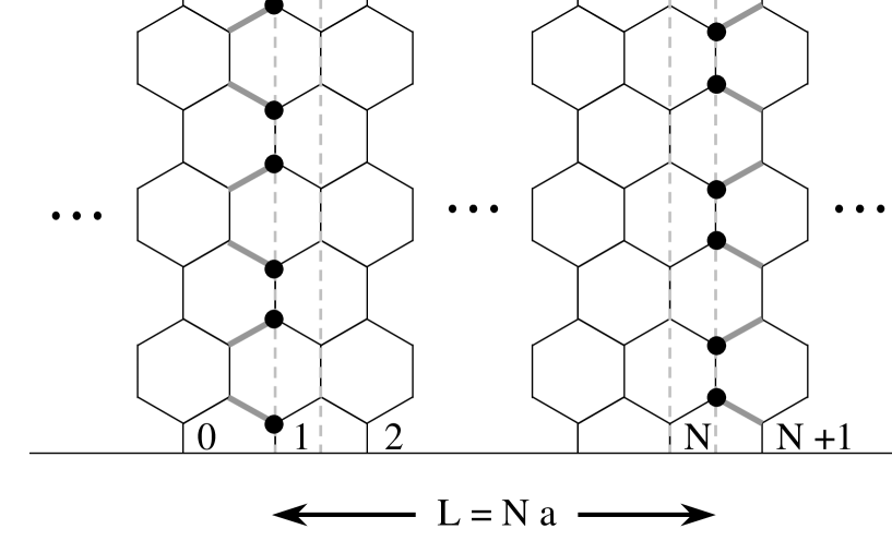
In this paper, on the other hand, we consider this problem in more detail, using a real-space approach. Such an approach intrinsically takes into account the interference phenomena due to multiple reflections from the boundaries. We show, that in some cases the diamond structure can be split and double diamond patterns may appear. For simplicity, we assume that the external electrodes (called also leads in the following) and the sample (central part) are made of similar SWCNTs. Thus, the whole model system consists of semi-infinite left and right leads and the central part of finite length. The interfaces (contacts) between the electrodes and the sample are considered as defects and are modeled by appropriate on-site and hopping parameters, which differ from the reference bulk values. In the experimental situation of Ref.[7] metallic Au/Cr electrodes were used. However, the key features of electronic transport studied there were due to the central part (sample) and its contacts to the electrodes. The electrodes themselves were thick enough to be considered as ideal leads. In our case such ideal leads are simulated by defect-free SWCNTs. In both cases the contribution of electrodes to the total resistance is negligible, and therefore one may expect that our results describe properly the experimental observations.
We adopt here the standard single-band tight-binding Hamiltonian to describe the carbon nanotubes with one -electron per carbon atom
| (1) |
where and stand for orbitals related to the nanotube unit cells (or principle rings, in analogy to principle layers exploited in layered structure calculations [8]). It is a very convenient way of ordering structural units which enables one to express the Hamiltonian in a block-tridiagonal form. The off-diagonal matrices are denoted by , whereas the on-diagonal ones by . The rank of the blocks is equal to the product of the number of rings within the unit cell times the number of circumferential carbon atoms. In the case of () armchair structures there are two carbon rings in the unit cell (bi-ring), each having atoms, thus the product gives atoms. It is noteworthy to stress in this context that within the ballistic regime, when there are neither impurities nor thermal excitations in the system, the conductance of armchair SWCNTs does not depend on their circumference, since it usually remains fully determined by just two energy bands which cross the Fermi energy. This is the case also in our situation, because for bias voltages of our interest higher energy bands do not enter the ’transport window’ () around the Fermi energy, except for huge nonotube diameters corresponding to .
The number of diagonal blocks in the Hamiltonian is equal to the length of a nanotube expressed in lattice constant units (). This is because for armchair structures there is just one bi-ring per lattice constant (see Fig. 1). Altogether, for armchair nanotubes of lengths , this gives a rank of the whole Hamiltonian up to 8000, i.e 24000 for considered hereafter. Fortunately, owing to the recursive Green function method this problem is still tractable. The recursive algorithm proceeds in the following steps:
(i) The left and right surface retarded Green functions (, ) are calculated by means of the standard iteration technique. Incidentally, any techniques which require inversion of the matrices are useless in our case because for the nearest neighbor hopping approximation the matrices are singular.
(ii) Going from down to , the remaining Green functions are found from
| (2) |
(iii) The total Green function can then be found as follows
| (3) |
(iv) The above specified matrix elements of are sufficient to express conductivity via the transmission matrix given by (cf. [9])
| (4) |
with
and the trace taken over all orbitals in the unit cell. It is worth to point out that the transmission matrix includes all the relevant interference effects.
Restricting ourselves to phase-coherent transmission, and assuming a constant potential within the whole sample (central electrode), we calculate the current from the following formula
| (5) |
where is the zero temperature Fermi-Dirac distribution function, and is the additional electrostatic energy in the central electrode generated by the gate voltage (we assume that only the central part is subject to the gate voltage). Hence, the differential conductance reads
| (6) |
Following Liang et al. [7] we assume that for symmetric contacts the access charge in the central electrode scales with as
| (7) |
where . Equation (7), when combined with the estimate of in terms of the density of states , leads to the universal relation between the gate voltage and the average potential energy
| (8) |
where stands for the capacitance per unit length of the sample (m-1 according to [7]), and is the Fermi velocity related to the slope of the energy level intersecting the Fermi energy (1.67meVm).
Equations (4) and (6) form the basis for our analysis of the differential conductance of armchair nanotubes. Our approach – as a real-space method – makes it possible to model arbitrarily the sample and the contacts, while keeping the external leads ideal. The contacts will be considered as defects in the otherwise perfect structure (disregarding the gate voltage). So far, tight-binding studies of nanotubes have focused on diagonal disorder and topological defects related to bending and twisting of nanotubes [10, 11, 12, 13, 14]. No systematic studies taking into account both diagonal and off-diagonal disorder in the presence of charging effects in the sample have been carried out yet, to our knowledge. The recursive algorithm presented above enables us to handle very complex structures, with arbitrary distribution of the hopping integrals and on-site potentials in the sample. However, in our case we vary only the parameters of the contacts, i.e., the contact nearest neighbor hopping integral (which enters the left and right corners of the matrices and , respectively) and the on-site potential energy (that comes to the respective upper and lower semi-diagonals of and ). Thus, we have just two fitting parameters related to the contacts, while all the nearest neighbor hoppings are set equal to , and all the atomic on-site energies in the leads are set equal to zero, whereas in the sample the on-site energies are increased by due to charging caused by the gate voltage.
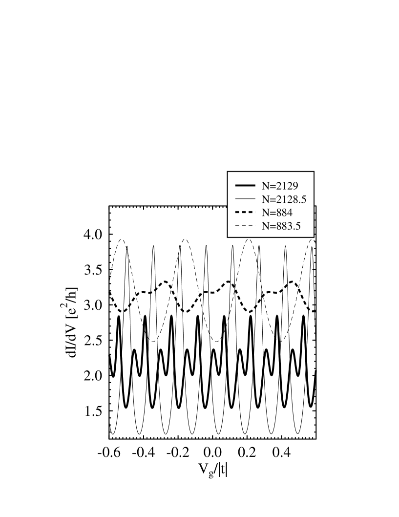
Conductance of a ballistic conductor oscillates as a function of length, but it does not decay (non-ohmic behavior) [16]. The key role played by the length consists in introducing an energy scale determined by the separation of energy levels. This is of crucial importance in the Coulomb blockade and in the Kondo regimes. It is also relevant in the strong coupling limit, and determines the periods in conductance oscillations with and . Another noteworthy point is that armchair SWCNTs show a conductance peak with a period , as their length varies. The physics standing behind this is quite simple and is due to the existence of zero energy eigen-value which coincides with the Fermi energy for such a length (in the ideal case, allowed values for a quantized wave vector include then [13]). We will see that there is a reminiscence of this behavior even when SWCNTs have modified interface parameters and are coupled to external electrodes. Our approach which makes also possible to sample SWCNT lengths equal to odd multiples of (single inter-ring spacing) shows that a fundamental quasi-period is rather then , confirming thereby an earlier observation of Ref. [15] in the context of energy spectra of isolated SWCNT segments. To be more specific, we present our results for nanotubes 884 and 2129 long (220 nm and 530 nm, as in Ref. [7]), which contain an even number of rings (integer number of elementary bi-rings), and also for nanotube lengths incommensurate with the lattice constant (883.5 and 2128.5).
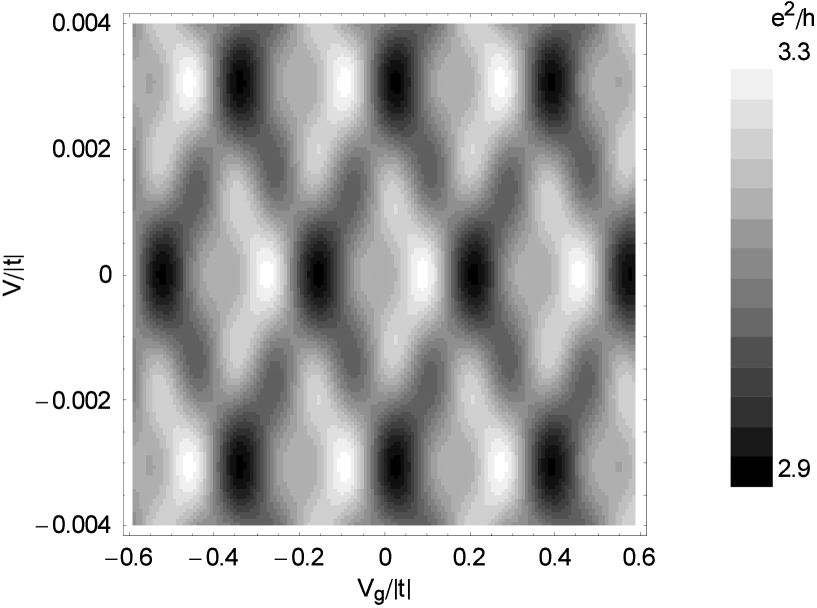
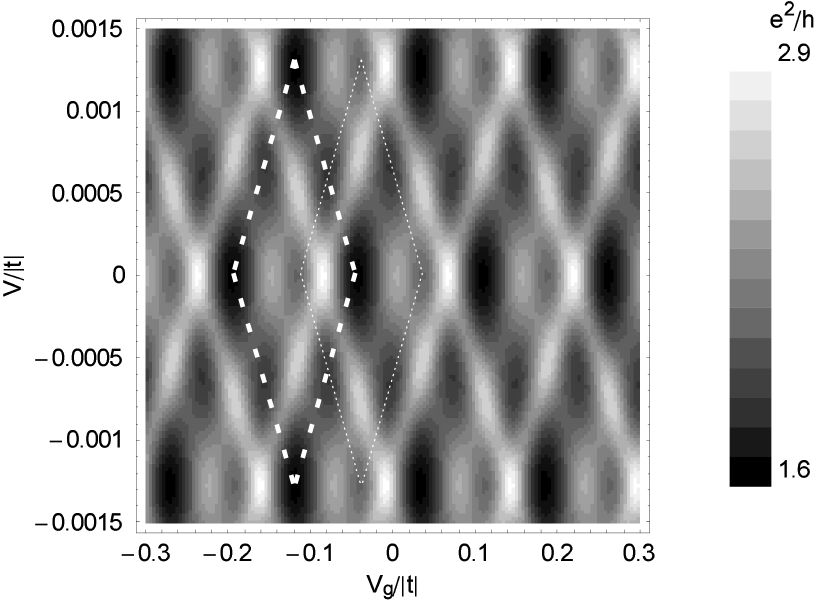
Our main results are presented in Figs 2 and 3 in a form of two-dimensional gray-scale density plots representing the conductance as a function of the bias and gate voltages. In order to convert and to Volts they should be multiplied by in eV (typically 2.7 [17]). We have chosen the parameters for the contact hopping integral across the interfaces and the on-site potential at the inner interface rings of carbon atoms so as to obtain variations of the conductance values similar to those of Ref.[7]. We have found that this would not be possible with only one fitting parameter, no matter whether or . The parameters we use are: and for Fig. 2, and and for Fig. 3. The results presented in Figs 2 and 3 agree with the experimental data in terms of both the conductance values and the periods in and . The large value of conductance indicates an almost perfect ballistic transport. Moreover, the periods in and are determined by the interlevel spacing as expected in the ballistic regime, whereas in the Coulomb blockade regime, the periods would be mainly determined by charging energy. For the periods in the bias voltage, , we have found (for ) 16.7 mV and 6.8 mV, which agree with the estimated values from the positive interference condition, , giving 15.2mV and 6.78mV for the 220 nm and 530 nm SWCNTs, respectively. The corresponding experimental values of Ref.[7] are 13mV and 7mV. Thus, the calculated interference patterns can be indeed interpreted in terms of multiple electron reflections and superposition with the phase change corresponding to the round trip length and the wavelength . Some discrepancies concerning the phases and certain irregularities present in experimental data are probably due to different external electrodes used in Ref.[7] and deviation of real systems from ideal ballistic conductors.
A detailed analysis of our results reveals new features in the diamond structure, like for instance the double-diamond patterns, indicated by dashed lines in Fig. 3. Such patterns originate from reflection conditions at the interfaces and are more pronounced when the contact hopping integral differs considerably from the ideal value , as it can be seen in Fig.3, in contrast to Fig.2 (with smaller ). This is illustrated in more detail in Fig.4. The thick solid line is there a cross-section of Fig. 3 and its main minima are related to the dominant diamonds, whereas the local minima to the faint ones. For a nanotube in length, represented by the thin full line, only main minima are present, implying the appearance of just one type of diamonds. A similar scenario holds for , and long SWNTs (dashed curves in Fig. 4), but then the shallow dips (shoulders) of the thick dashed line are too small for the diamond sub-structure to be visible in Fig. 2. The appearance of the double-diamond structure may be explained in terms of symmetry induced resonant level degeneracy. Our structural models are symmetric by construction (see Fig. 1) even if the contact parameters differ considerably from the reference ones. Now, for varying SWCNT lengths the on-resonance conductance peak (close to ) will be split as a result of lifting of degeneracy by modified boundary conditions at the interfaces. The process will repeat with a quasi-period .
There is no evidence of the double diamond sub-structure in the experimental data of Ref.[7]. However, our results indicate that such a structure may be observable. The experimental data for 530 nm long SWCNTs show clearly a superstructure imposed on the basic diamond structure. Such a superstructure may result from superposition of at least two different oscillation periods in both bias and gate voltages. Since the periods depend on the sample length, one may expect that the superstructure is due to some additional defects inside the sample. Such defects may produce a diamond structure with longer periods. When imposed onto the main pattern, it can then lead to the patterns observed experimentally. This is a possible explanation of the experimental results (for 530 nm SWCNT), but probably not the only one. There might be some other physical mechanisms producing similar effects, which have not been included in our calculations.
In conclusion, our calculations yield correct values of both the conductance oscillation periods and the conductances themselves. Apart from this, our results show that the diamond structure patterns for are very sensitive to conditions at the contacts between the sample and external leads. The off-diagonal disorder, described by a modified hopping integral across the interfaces, acts as moderate energy barriers (strong coupling or weak confinement limit). The periods in the bias and gate voltages are determined by separation of the energy levels, and are inversely proportional to the sample length. The diagonal defects, introduced by setting extra on-site energy on the first ring of the nanotube and on the last one, act as an additional reflecting factor responsible for asymmetry with respect to . These two kinds of defects, only when both taken into account, give satisfactory magnitudes of the conductance values for various SWNT lengths. The double-diamond paterns may be expected in the ”on-resonance” case, i.e. for such a length which makes the density of states have a peak at the Fermi energy.
Acknowledgments We thank the Poznań Supercomputing and Networking Center for the computing time. The support through the Research Project 5 P03B 091 20 is also acknowledged (JM).
REFERENCES
- [1] S. Iijima, Nature 354, 56 (1991).
- [2] M.S. Dresselhaus, G. Dresselhaus, and P. Avouris (eds), Carbon nanotubes – Synthesis, Structure, Properties, and Applications, (Springer, Berlin, 2001).
- [3] C. Dekker, Physics Today May 22 (1999).
- [4] P.L. McEuen, Physics World 13, 21 (2000).
- [5] H.W.Ch. Postma, T. Teepen, M. Grifoni, and C. Dekker, Science 293, 76 (2001).
- [6] J. Nygard, D.H. Cobden, and P.E. Lindelof, Nature 408, 342 (2000).
- [7] W. Liang, M. Bockrath, D. Bozovic, J.H. Hafner, M. Tinkham, and H. Park, Nature 411, 665 (2001).
- [8] A. Umerski, Phys. Rev. B 55, 5266 (1997).
- [9] R. Lake, G. Klimeck, R.C. Bowen, and D. Jovanovic, J. Appl. 81, 7845 (1997).
- [10] L. Chico, L.X. Benedict, S.G. Louie, and M.L. Cohen, Phys. Rev. B 54, 2600 (1996).
- [11] M.P. Anantram and T.R. Govindan, Phys. Rev. B 58, 4882 (1998).
- [12] T. Kostyrko, M. Bartkowiak, and G.D. Mahan, Phys. Rev. B 60, 10735 (1999).
- [13] D. Orlikowski, H. Mehrez, J. Taylor, H. Guo, J.Wang, and G. Roland, Phys. Rev. B 63, 155412 (2001).
- [14] A. Rochefort, P. Avouris, F. Lesage, and D. R. Salalub, Phys. Rev. B 60, 13824 (1999).
- [15] A. Rochefort, D. R. Salalub, and P. Avouris, Phys. Rev. Chem. B 103, 641 (1999).
- [16] S. Datta, ”Electronic transport in mesoscopic systems”, Cambridge University Press, Cambridge (1995), Eds., H. Ahmed, M. Pepper, and A. Broers.
- [17] C.T. White and T.N Todorov, Nature 393, 240 (1998).
List of Figures
lof