Analysis of integrated single-electron memory operation
Abstract
Various aspects of single-electron memory are discussed. In particular, we analyze the single-electron charging by Fowler-Nordheim tunneling, propose the idea of background charge compensation, and discuss the defect-tolerant architecture based on nanofuses.
It is a common wisdom now that because of the size reduction of the components of integrated digital devices, the effects of charge discreteness will eventually become important. And there is a strong belief that the correlated tunneling of single electrons [1, 2] in such ultradense devices can provide the physical basis for the new principle of their operation (see, e.g., Refs. [3, 4]).
There are two main possible areas of prospective digital single-electronics: logic and memory devices. The theoretical analysis shows [3, 4] that the single-electron memory is much easier for the implementation than the logic. The basic reason is that a logic device is necessarily a complex system consisting of many gates interacting in a specific way, while memory cells are independent, each of them being a simple circuit. The operation of the logic requires some kind of voltage amplification (which can be also done parametrically [5]) to pass information from gate to gate. In contrast, in the memory the storage of information can be done in a passive way, and for the readout only some sensing of the storage contents is sufficient (the amplification can be done at the next stage, common for many memory cells).
As an example, the single-electron transistor (SET) can amplify the voltage only at temperatures[6] where is the total capacitance of the SET central island while in the sensing mode it can be used at temperatures up to (the modulation amplitude of the SET is still more than 10% at this temperature). The possibility to use significantly higher temperatures is very important for single-electronics. In addition, the problem of random background charge can be solved for memory (while for the logic no reasonable solutions have been proposed so far) that is also very important for integrated circuits. The basic idea of the background-charge-insensitive operation proposed in Ref. [7] is to use oscillating output of the SET as a response to the ramp-up input signal so that the phase of the oscillations (which can be unpredictably shifted by the background charge) is not important. The input signal is generated during destructive readout of logical “1”, which erases the few-electron charge stored at the floating gate close to the SET, while there is no signal if there was no stored charge (logical “0”). The low-temperature prototype of the background-charge-insensitive single-electron memory has been demonstrated experimentally.[8]
There have also been a considerable number of experiments (including room-temperature experiments) on single-electron memory using different ideas (see, e.g., Refs. [9, 10, 11, 12, 13, 14, 15, 16, 17, 18, 19, 20, 21, 22, 23]). While most of them would have principal difficulties at the realistic level of integration, the experimental success supports the optimistic prospect of technologically practical single-electron memory.
In this paper we discuss various single-electron effects in the memory devices. We consider the DRAM-like and nonvolatile single-electron memories based on the charge storage at the floating gate. (The SRAM-like single-electron memory [6] suffers from the same difficulties as the single-electron logic.) In particular, we discuss the interplay between Coulomb blockade and Fowler-Nordheim tunneling, propose the idea of background charge compensation, and propose the defect-tolerant architecture for single-electron memory based on nanofuses and nanoshorts.
Let us assume that the digital information is stored in the form of an electric charge. Then there are at least three aspects, for which single electrons can be important. First, the digital bit can be represented by few or even only one electron. Second, the Coulomb blockade can be used as a mechanism providing bistability of the memory cell. Third, the readout can be done using a single-electron principle, for example, the stored charge can be sensed by the SET. Let us consider these aspects in more detail.
The bit representation by a single electron provides the lowest energy dissipation for write/erase operations and can in principle be performed even when the “floating gate” has the size as small as one atom. Also, single electron storage is the physical limit of electronics, and in this respect it is technologically and psychologically important. Notice, however, that in this case the bit information can be instantaneously destroyed by only one leakage event. As a consequence, the probability of error is suppressed only linearly with the decrease of the time before the readout (in contrast to almost exponential suppression for continuous leakage). This also leads to impossibility of the information refreshing using simple read-write back procedure, since there is no bit “aging”.
The straightforward way to improve reliability is to use redundancy; for example, to store the bit simultaneously in three memory cells and use the majority principle at readout. However, obviously it is simpler to use redundancy inside the memory cell, which is to represent bit by three stored electrons, so that the leakage of one electron is allowed. This decreases the leakage error probability down to , where is the error probability for the one-electron cell, and makes possible the information refreshing (since scales as a square of retention time). Further increase of the number of stored electrons leads to further reduction of the error probability. One can expect that the optimal number of stored electrons is somewhere between 5 and 30. Notice, however, that this number should be controlled with single-electron accuracy: the usual Poisson distribution is unacceptably wide when .
A different method to improve the reliability of a memory cell with one electron per bit is to readout simultaneously a block of cells and use the idea of “control sums”. For example, using extra cells as control sums for columns and rows of a block of cells, one can easily restore the loss of one bit and, hence, reduce the error probability down to . Additional control sums can restore the loss of more than one bit, that suppresses further the error probability. (Actually, the use of columns, rows, or diagonals of a block for control sums is obviously not the best way of introducing redundancy. Using standard coding algorithms [24] one can restore up to 11% of errors by doubling the numbers of memory cells.) So, for the single-electron representation of a bit, the reliable information storage can also be achieved, however, the few-electron representation of a bit (inside one memory cell) makes it significantly simpler and seems more natural for random access memory.
The charge storage requires very low leakage rate for both logical states while write/erase time should be sufficiently fast. In the present-day DRAMs this is achieved by the use of field-effect transistor (FET) as a switch. Unfortunately, the SET cannot replace FET for this purpose because of significant cotunneling rate,[1] so other principles are necessary. A promising principle is the control of the tunnel barrier by the gate electrode.[25] For single-electron memory a similar principle has been used in the experiments or Refs. [11, 16] (which have been discussed using the terminology of multiple-tunnel-junction SET).
Besides the gated operation of charge write/erase procedure, one can consider non-gated operation similar to that used in the conventional nonvolatile memories.[26] The idea is to use a threshold-like behavior of the charging rate as a function of the voltage between the storage floating gate and the word (or bit) line. Then the long retention time is achieved if the voltage due to charging of floating gate capacitance as well as the half-select write/erase voltage are below the threshold, while fast write/erase operation occurs when the external full-select voltage exceeds the threshold.
A natural for single-electron memory idea is to use the Coulomb blockade for such a threshold. For example, it can be provided by the array of small-capacitance tunnel junctions similar to that used in single-electron traps (see, e.g. Ref. [10] and references therein). Unfortunately, the random background charges lead to unacceptably wide distribution of the Coulomb blockade thresholds and Coulomb blockade barrier heights.[3]
Another way is to use the threshold-like dependence of the conventional Fowler-Nordheim tunneling. The problem is that in this case there is no sharp threshold, and as a consequence the ratio of the retention and write/erase times is not sufficiently large. The situation can be significantly improved by the use of the tunnel barriers of crested shape [7, 27] so that not only the width but also the height of the barrier decreases with the applied voltage. The crested barrier can be fabricated using -doping, composition grading, or layered structure.
We have studied the single-electron charging of the floating gate by Fowler-Nordheim tunneling using the following simple “orthodox” model.[1] The tunneling rate is determined by the effective voltage
| (1) |
where is the contribution due to externally applied write/erase voltage, is the number of extra electrons on the floating gate which changes during charging, is the background charge, and is the storage floating gate capacitance. For the “seed” I-V curve we used the model of Ref. [28] applied to the 4nm/5nm/4nm trilayer crested barrier with parameters corresponding to Si/Si3N4/AlN/Si/Si3N4/Si. The inset in Fig. 1 shows the classical recharging time (defined as ) as a function of the voltage across the barrier.
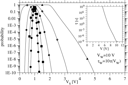
Since the tunneling is a stochastic process, the number of stored electrons after the application of voltage during time , is random. So, after the external voltage is removed, the potential of the floating gate can be characterized by the probability distribution. Fig. 1 shows numerically calculated distribution of for V, , and several values of the single-electron voltage : 0.03 V (dots), 0.1 V (squares), 0.3 V (diamonds), 1 V (crosses), and 3 V (triangles). The symbols correspond to the background charge while the lines show the probability densities after the averaging over random (normalized in a way that the lines go through the symbols).
One can see that the probability distribution is relatively narrow when is small, and in this case there is essentially no difference between the random and well-defined . The distribution width grows with , and in the case the fluctuations are unacceptably strong for the reliable information storage. The curve width continue to grow when becomes larger than typical of the classical charging. However, if is well-defined, the probability distribution collapses into single well-predictable value of . Moreover, the voltage in this case can be considerably larger than for small , that can be useful for the readout. It is important that the effective voltage which determines the retention time is (less than ); so for , large , and one stored electron (the upper triangle in Fig. 1) this voltage is exactly zero that can significantly improve the charge retention. The probability of a “dynamic” error due to finite write/erase time in the symmetric one-electron case () decreases exponentially with , where is determined by the full write voltage . This is obviously an advantage [13] in comparison with the case of small , in which the voltage gradually decreases in the process of charging, gradually decreasing the charging rate.
The analysis above shows that there are two preferable modes of operation. Either the bit should be represented by many ( 10) electrons (then there is no need to control ) or it should be just one electron (and is well-controlled), while in the few-electron regime the fluctuations of the stored charge are very strong. As one can see from Fig. 1, the typical voltage in the one-electron regime should be about few volts that obviously suggests the use of single atoms as “floating gates” (the randomness of the location can be avoided using self-assembly). For single atoms the fluctuations of are naturally small since the chemical environment is well defined. (Actually, for single atoms the “orthodox” theory should be modified [29], and instead of fluctuations we need to consider the variation of the electron affinity.) Using the language more natural for atoms, the best case corresponds to the impurity energy exactly at the Fermi level, so that both occupied and empty states are equally stable. Notice that the use of single atoms can be easily combined with the idea of few-electron bit representation if few atoms (located sufficiently far from each other) per memory cell are used.
Now let us discuss the readout of the stored charge. There is an experimental evidence [14] supported by the theoretical analysis [30] that FET can be used for sensing the charge at the size scale down to 10 nm. Another option (which seems to be preferable only at the size scale below 10 nm) is the use of SET. Besides the problem of low operation temperature which will become less severe when the few-nm technology is available, another principal problem for integrated SET devices is the background charge fluctuations.[3, 4] One proposed solution [7] is the background-charge-insensitive operation. Here we propose a different solution.
The idea is to tune (compensate) individually the background charge of each SET. From the first sight this seems impossible in an integrated circuit. However, the simple uniform architecture of the memory allows the local self-compensation procedure. Instead of tuning the background charge by the voltage applied to an extra gate (that is typically used in present-day single-electron experiments) we propose to use extra floating gate. Fig. 2 shows the memory cell consisting of storage floating gate (it can be replaced by single atoms as discussed above), SET to sense its charge, and -compensating floating gate (CFG). If the dimensionless coupling between the CFG and the central island of the SET is about 0.1, then placing the proper number of electrons on CFG we can control with the accuracy of that is sufficient for predictable readout from the SET.
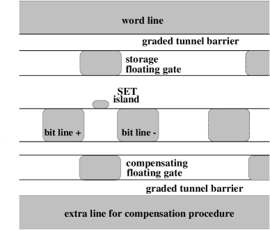
The CFG is charged by the Fowler-Nordheim tunneling from the extra word line (see Fig. 2) and the amount of charge is determined by the voltage applied between this line and bit lines connected to SET. The compensation procedure can be done in the following way. The storage floating gate is prepared in logical state “0”, the SET is biased, and the ramp-up voltage is applied to one of the word lines (or both). The SET output performs the oscillations, the phase of which carries the information about . After amplification by the sense amplifier connected to the bit line, this signal is used to determine the proper magnitude of the voltage pulse to be applied between compensating word line and bit lines (an iterative sequence of trials and tests can be useful). The compensating pulse should be applied to the bit lines to allow simultaneous compensation procedure for all cells connected to the same word line. Since the compensation procedure requires the charge erasure from the storage gate, it can naturally be combined with the information refreshing.
Besides the presence of the CFG and extra word line, the layout and the basic parameters of the -compensated single-electron memory is similar to that of background-charge-insensitive memory of Ref. [7]. In particular, the room temperature operation can also be achieved at 4 nm minimum feature size (20 nm 40 nm total area per cell). The important advantage in comparison with the background-charge-insensitive memory is the possibility of nondestructive readout. This also implies the reduction of the stored charge and/or coupling between the SET and storage gate, because this charge reduced to the SET input should no longer correspond to several Coulomb oscillations but only to a fraction of the period instead.
If the SET operates in the high-temperature “analog” regime () then the destructive readout remains the only reasonable option. The SET should be tuned to the most sensitive operation point of the control characteristic and the output SET current before and after the attempted bit erasure should be compared. It is important that other SETs connected to the same bit line are also biased and contribute to the current noise. The maximum number of SETs per sense amplifier is determined by the bandwidth and acceptable signal to noise ratio, and in this case is comparable to that of background-charge-insensitive memory, i.e. . In the low-temperature regime () the current and noise from half-selected SETs (biased but not selected by proper gate voltage) can be strongly suppressed by the Coulomb blockade, so the SET can essentially operate as a switch. This provides much better signal to noise ratio and allows for a nondestructive readout as well as a significant increase of in -compensated single-electron memory.
The architecture of the single-electron memory should obviously differ from that of conventional memory. First, if the SET is used for the readout, then the relatively high output impedance of the SET requires quite short local bit lines in order to reduce their charging time. Second, with the strong decrease of the feature size and possible use of the molecular electronics technology, one can expect the reduction of the yield per memory cell, [31] so the architecture should be able to tolerate significant fraction of defects. We propose here a novel defect-tolerant memory architecture based on nanofuses and nanoshorts (which can be useful for any ultradense memory).
The main idea is the local physical rerouting of the bit (or word) lines in order to avoid defective cells. In contrast to the logic, the uniform memory organization allows us to test each memory cell (of course, such testing can be done in parallel for many cells). For significant fraction of defects, any long bit line would contain defects. So only rejection of relatively small pieces of the line is possible and the architecture should necessarily be local. The significant fraction of defects also makes it impossible to store the information about the defective cells and then switch the addresses logically, since it could require storage space comparable to the total available memory. The problem can be solved by physical rerouting of bit lines to replace the relatively short defective pieces by good ones from the local reserves. This is done once during the testing procedure while from the outside (global level of hierarchy) all the lines look nondefective.

Fig. 3 illustrates the idea of rerouting. The cells are organized in blocks of the relatively small size , where cells are normally used while cells are “in reserve”. If during the testing a cell is found to be defective, the corresponding line of cells should be replaced by the line from reserve. For this purpose we need two types of switches: nanofuses (which can be blown to disconnect the line) and nanoshorts (which can connect lines). Notice that each switch is used at most once, so it can be a quite simple and therefore reliable nanoscale device. The importance of nanoswitches for any type of nanoelectronics has been previously emphasized in Ref. [31] and the experimental progress has been already reported.[32]
The blown nanofuse disconnects the defective line of cells; instead, the switched nanoshort connects another line of cells to the same global bit line so that from outside the addressing does not change. Since the global bit line should pass through much more than cells, we either need to return to the main bit line after the detour, switching another nanofuse/nanoshort pair, or use the idea of local -long branches connected to the global bit line “in parallel”.
The optimal values of , , and obviously depend on the expected fraction of defective memory cells. Notice that the idea works even if is comparable to unity. (In this case one can use , , and sufficiently large .) If in a bad luck case lines prepared for the replacement are not sufficient for defect-free operation, the rerouting of a longer piece of the bit line can be used at the next level of hierarchy.
The switching of nanofuses and nanoshorts requires extra wires for their selection, which are not discussed here. Also, we assumed perfect wires and nanoswitches. This assumption seems to be reasonable, since the memory cell is a more complex device and, hence, has much larger chance to be defective. The rare defects of wires, nanofuses, and nanoshorts can be treated by conventional means.
In conclusion, we have discussed various aspects of the single-electron memory operation. First, the analysis of the Fowler-Nordheim charging of a floating gate in a single-electron regime shows that the most preferable mode of operation is when two logical states differ by exactly one electron on a floating gate, which itself has the background charge . This suggests the use of single impurity atoms at the Fermi level as floating gates. Second, the operation of the single-electron transistors for memory readout can be significantly improved by using the proposed -compensation procedure employable in integrated design. Third, the proposed defect-tolerant memory architecture based on nanofuses and nanoshorts can provide reliable operation even in the case of significant fraction of defective memory cells. Leaving aside the major present-day obstacle for single-electron memory, which is the need for reliable few-nm technology, the overall prospect of the development of integrated single-electron memory within next 10-20 years seems to be quite optimistic.
The author thanks K. K. Likharev for numerous fruitful discussions. The work was supported by the Semiconductor Research Corporation Contract No. 2000-NJ-746.
REFERENCES
- [1] D. V. Averin and K. K. Likharev, in: Mesoscopic phenomena in solids, ed. by B. Altshuler et al. (Elsevier, Amsterdam, 1991), Ch. 6.
- [2] Single charge tunneling, edited by H. Grabert and M. H. Devoret (Plenum, New York, 1992).
- [3] K. K. Likharev, Proc. IEEE 87, 606 (1999).
- [4] A. N. Korotkov, Int. J. Electronics 86, 511 (1999).
- [5] K. K. Likharev and A. N. Korotkov, Science 273, 763 (1996); J. Appl. Phys. 84, 6114 (1998).
- [6] A. N. Korotkov, R. H. Chen, and K. K. Likharev, J. Appl. Phys. 78, 2520 (1995).
- [7] K. K. Likharev and A. N. Korotkov, in Proceedings of ISDRS’95 (Charlottesville, VA, 1995), p. 355; VLSI Design 6, 341 (1998).
- [8] C. D. Chen, Y. Nakamura, and J. S. Tsai, Appl. Phys. Lett. 71, 2038 (1997).
- [9] K. Yano, T. Ishii, T. Hashimoto, T. Kobayashi, F. Murai, and K. Seki, IEEE Trans. on Electron. Dev. 41, 1628 (1994); K. Yano et al., Proc. IEEE 87, 633 (1999).
- [10] P. D. Dresselhaus, L. Ji, S. Han, J. E. Lukens, and K. K. Likharev, Phys. Rev. Lett. 72, 3226 (1994).
- [11] K. Nakazato, R. J. Blaikie, and H. Ahmed, J. Appl. Phys. 75, 5123 (1994).
- [12] A. Fujiwara, Y. Takahashi, K. Murase, and M. Tabe, Appl. Phys. Lett. 67, 2957 (1995); Y. Takahashi et al., Jpn. J. Appl. Phys., 38 (Part 1), 2457 (1999).
- [13] S. Tiwari, F. Rana, H. Hanai, A. Hartstein, E. F. Crabbe, K. Chan, Appl. Phys. Lett. 68, 1377 (1996); S. Tiwari, F. Rana. K. Chan, L. Shi, and H. Hanafi, Appl. Phys. Lett. 69, 1232 (1996).
- [14] L. Guo, E. Leobandung, and S. Chou, Appl. Phys. Lett. 70, 850 (1997).
- [15] A. Nakajima, T. Futatsugi, and N. Yokoyama, Appl. Phys. Lett. 70, 1742 (1997).
- [16] Z. A. K. Durrani, A. C. Irvine, H. Ahmed, and K. Nakazato, Appl. Phys. Lett. 74, 1293 (1999); A. C. Irvine, Z. A. K. Durrani, and H. Ahmed, J. Appl. Phys., 87, 8594 (2000); H. Mizuta et al., Nanotechnology 12, 155 (2001).
- [17] S. V. Lotkhov, H. Zangerle, A. B. Zorin, and J. Niemeyer, Appl. Phys. Lett. 75, 2665 (1999).
- [18] A. Dutta, S. P Lee, S. Hatatani, and S. Oda, Appl. Phys. Lett. 75, 1422 (1999).
- [19] H. Sunamura, T. Sakamoto, Y. Nakamura, H. Kawaura, J.-S. Tsai, and T. Baba, Appl. Phys. Lett. 74, 3555 (1999).
- [20] I. Kim, S. Han, K. Han, J. Lee, H. Shin, IEEE Electron Dev. Lett. 20, 630 (1999); Jpn. J. Appl. Phys. 40 (Part 1), 447 (2001).
- [21] K. H. Yoo, J. W. Park, J. Kim, K. S. Park, S. C. Oh, J. O. Lee, J. J. Kim, J. B. Choi, and J. J. Lee, Appl. Phys. Lett. 74, 2073 (1999); J. Kim et al., Jpn. J. Appl. Phys. 39 (Part 1), 4826 (2000).
- [22] K. Matsumoto, Y. Gotoh, T. Maeda, J. A. Dagata, and J. S. Harris, Appl. Phys. Lett. 76, 239 (2000).
- [23] E. Kapetanakis, P. Normand, D. Tsoukalas, and K. Beltsios, Appl. Phys. Lett. 80, 2794 (2002).
- [24] R. G. Gallager, Information theory and reliable communication (Wiley, NY, 1968).
- [25] J. Tucker, C. Wang, and P. S. Carney, Appl. Phys. Lett. 65, 618 (1994).
- [26] Nonvolatile semiconductor memories, ed. by C. Hu (IEEE, New York, 1991).
- [27] K. K. Likharev, Appl. Phys. Lett 73, 2137 (1998).
- [28] A. N. Korotkov and K. K. Likharev, Appl. Phys. Lett. 75, 2491 (1999).
- [29] D. V. Averin, A. N. Korotkov, and K. K. Likharev, Phys. Rev. B 44, 6199 (1991).
- [30] Y. Naveh and K. K. Likharev, Superlat. Microstr. 27, 111 (2000).
- [31] J. R. Heath, P. J. Kuekes, G. S. Snider, and R. S. Williams, Science 280 1716 (1998).
- [32] C. P. Collier, E. W. Wong, M. Belohradsky, F. M. Raymo, J. F. Stoddart, P. J. Kuekes, R. S. Williams, and J. R. Heath, Science 285, 391 (1999).