Single Carbon Nanotube–Superconductor
Entangler:
noise correlations and EPR states.
Abstract
We propose a device which implements a solid-state nanostructured electron entangler. It consists of a single-walled carbon nanotube connected at both end to normal state electrodes and coupled in its middle part to a superconducting nanowire. Such a device acts as an electronic beam splitter for correlated electrons originating from the superconductor. We first show that it can be used to detect positive (bosonic–like) noise correlations in an fermionic system. Furthermore, it provides a source for entangled electrons in the two arms of the splitter. For generating entangled electron states, we propose two kinds of setup based either on spin or energy filters. It respectively consists of ferromagnetic pads and of a system of electrostatic gates which define quantum dots. The fabrication of this device would require state-of-the-art nanofabrication techniques, carbon nanotube synthesis and integration, as well as atomic force microscopy imaging and manipulation.
pacs:
PACS 03.65.Ud, 72.70.+m, 74.50.+rI Introduction
In the last decade, photon entanglement has triggered the proposition of new information processing schemes based on quantum mechanics [2]. Indeed emerging fields such as quantum cryptography and quantum communication [3, 4] are based on particle entanglement. On the other hand, concrete proposals for quantum computing, based on electron transport and electron interactions in condensed matter have been recently presented. [5, 6, 7]. Among them, devices taking advantage of the macroscopically coherent wave of superconductivity [8] are promising candidates for the practical realization of a fully solid-state quantum bit [9].
Recently, the proposal of Ref. [7] showed that the generation mechanism for entangled electrons pairs emerging from a superconductor could provide a rather robust alternative to photon entanglement. It was first shown [10] that a normal metal fork attached to a superconductor can exhibit positive correlations. Positive correlations had been attributed to photonic systems in the seminal Hanbury-Brown and Twiss experiment [11]. In our case, positive correlations arise because evanescent Cooper pairs can be emitted on the normal side, due to the proximity effect [12]. These Cooper pairs can either decay in one given lead, which gives a negative contribution to noise correlations, or may split at the junction on the normal side with its two constituent electrons propagating in different leads. This latter effect constitutes the justification for positive noise correlations. Moreover such a mechanism generates entangled and delocalized electron pairs[7]. Two electrons originating from a broken Cooper pair bear entangled energy and spin degrees of freedom. This provides a solid state analog of Einstein-Podolsky-Rosen (EPR) states which were proposed to demonstrate the non-local nature of quantum mechanics [13]. Both theoretical proposals – for positive correlations and for EPR entanglement in electronic systems – are in need for experimental observation. The purpose of the present paper is to define a solid-state device together with a detection setup of these both quantum effects. It is based on a Single Walled Carbon Nanotube (SWNT) coupled to a Superconducting electrode (nicknamed in the following the S-SWNT device).
Troughout the paper a single electron description of transport will be adopted. This choise is motivated in several ways. First, single electron scattering theories have been quite successful so far in describing the transport properties of carbon nanotubes. An example is the seminal Fabry-Perot experiment of Ref. [14] which can be interpreted with a ballistic propagation picture. Second, we intend here to describe a rather complex device: electrons are injected from a superconductor in a nanotube, possibly with additional scattering elements or filters. It therefore makes more sense to first enquire what the transport properties are from the scattering theory point of view, rather than to go immediately to a correlated electron description. Nevertheless, evidence of Luttinger liquid behavior in tunneling geometries involving metallic SWNTs has been proposed [15]. The experimental measurement of the tunneling characteristics [16] yields density of states exponents which are consistent with strong correlations. Below we address briefly when the single electron picture is expected to hold, and what features of Luttinger liquid theory could affect the S-SWNT device.
II Entanglement of electrons tunneling from a superconductor
A perturbative argument supports the claim that two electrons originating from the same Cooper pair are entangled. Consider two quantum dots (Energies ) next to a superconductor. The state of the latter is specified by the BCS wave function . Tunneling to the dots is described by a single electron hopping Hamiltonian:
| (1) |
with creates an electron with spin . Now let assume that the transfer Hamiltonian acts on a single Cooper pair. Using the T-matrix to lowest (nd) order, the wave function contribution of the two particle state with one electron in each dot reads:
| (2) | |||||
| (3) |
where, is the energy of a Bogoliubov quasiparticle. The state of Eq. (3) has entangled spin degrees of freedom, a result of the spin symmetry of the tunneling Hamiltonian. From the superconductor, can only produce singlet states in the dots. We now present a device where this entangled state propagates along metallic wires.
III Noise correlations in the S–SWNT device
Consider a system consisting of a superconducting electrode which is contacted locally to the middle of a single-walled carbon nanotube. (SWNT). Current can in principle be measured at each extremity of the 1D conductor. From the point of view of the Landauer–Buttiker scattering approach to quantum transport [17], it consists of scattering elements, including a “beam splitter”, and a normal superconductor interface (2). A more realistic drawing of this setup is also depicted in Fig. 3. Note that this device is analogous to the one used in the fermion analog of the Hanbury–Brown and Twiss experiment [18, 19], except that the electron source is a superconductor.
The scattering matrix which specifies the amplitudes of the incoming and outgoing states at the junction does not provide any information about entanglement, because of its single-electron character. Yet we argue here (and below) that entanglement is implicit in correlations measurements. The generation of entangled, non-local electronic states requires that a substantial fraction of Cooper pairs distribute their electrons in the two leads, rather than in the same one. A suggested diagnosis of the presence of Cooper pairs in the two arms of a nanotube lies in the noise correlator:
| (4) |
evaluated at zero frequency. Here, denotes the current operator in lead . The positive noise correlations predicted in a single channel NS junction[10] constitute a direct consequence of these tunneling processes. For the SWNT beam splitter, the presence of two propagating channels at the Fermi energy in each lead requires that we address the issue of channel mixing due to impurities/geometrical scattering. The addition of several transverse channels [20] may destroy the positive noise correlations which signal the presence of entangled electron pairs.
Because of the two channels in each lead, a scattering matrix fully characterizes this branched N-S junction (no spin-flip scattering). Denote by the scattering amplitude for a particle (, electron or hole) incident from channel associated with lead , transferred in channel of lead as a particle of type . Using the scattering formulation of quantum transport together with the Bogoliubov–de Gennes transformation [21], the zero frequency noise correlations below the gap become:
| (5) | |||
| (6) | |||
| (7) |
Our model device is depicted in the inset of Fig. 3. It is composed of four scattering elements. Perfect Andreev reflection occurs at the N-S interface (with no channel mixing), and two independent beam splitters (for electrons and holes) describe the connection to the SWNT. The splitters transmission to the two leads is controlled by a single parameter ( for maximal transmission) as in Ref. [10]. Channel mixing is then included within each tube using a numerical random matrix scheme [22], here represented by the two rectangles on the left hand side of Fig. 3. After specifying each S–matrix of the subsystems, those are combined to yield a S–matrix which characterizes the propagation of electrons and holes from to .
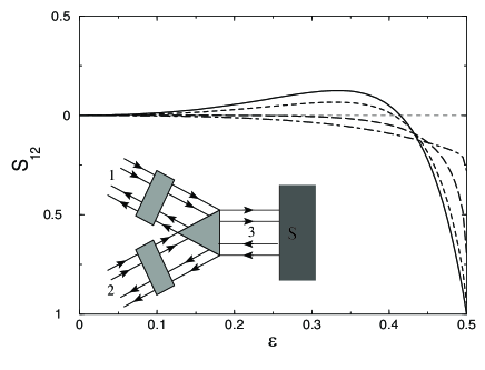
The scheme for including mode mixing and backscattering in a mode quantum wire generates numerically random (unitary) scattering matrices: , where is a random, Hermitian matrix. It only makes sense to compare different samples with the same amount of disorder. A perfect, -channel conductor can be described by a scattering matrix which is a block matrix with identity matrices on the off diagonal blocks, zero otherwise. The corresponding matrix can be found, but is not unique due to the periodicity of the exponential function. We generate unitary, random matrices by adding a small random perturbation to : , where is a random hermitian matrix with a unit norm. The limitation then insures that the S–matrix generated in this manner has an increased amount of disorder starting from . In this manner, samples with a specific conductance, or equivalently, a specific mean free path per sample length, are generated.
The zero frequency noise correlations are obtained using Eq. 7 and averaging over sample configurations. The results are illustrated by the curves of Fig. 2, which show the averaged zero frequency noise correlations as a function of the parameter which parameterizes the connection of the beam splitter to the two nanotube arms. The different curves correspond to varying degrees of channel mixing.
When an infinitesimal mixing or backscattering is included in each nanotube arm (weak disorder), positive noise correlations are observed as in Ref. [10] for a vast majority of the coupling parameter . For non zero , the disorder in the nanotube arms is increased, and it restricts the possibility for positive noise correlations. The positive correlations are mostly reduced in amplitude, while occurring for the same ranges of . The range of with positive correlations is reduced, and eventually vanishes completely for stronger mixing. Note that the disorder parameter lies in the strong scattering regime. Nevertheless, we conclude that this system is sufficiently robust because a weak amount of disorder does not entirely spoils the effect.
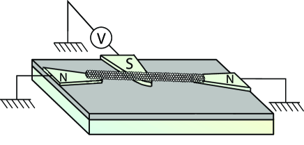
IV The S-SWNT device: a Cooper pair splitter
The practical implementation of this device [10] consists of a superconducting reservoir connected to two normal metal leads (see Fig. 3). Ballistic propagation in these normal leads is optimal for the detection of electron entanglement via a noise correlation measurement. The Single Walled Carbon Nanotube (SWNT) appears to be a good candidate for implementing the normal lead. Indeed SWNTs can be considered as quasi-ideal one dimensional electron waveguides[23, 24, 14], with either metallic or semiconductor behavior depending on their helicity. Metallic SWNTs have two propagating modes with equal velocity at the Fermi level and can exhibit quasi-ballistic transport [25]. On the other hand semiconducting SWNTs can be electrostatically [26, 27] or chemically doped [28] to make a single channel conductor, which is however more sensitive to disorder. Nanotubes also present the advantage that they can be reliably assembled into complex integrated circuits [29, 30] and withstand controlled intra-molecular functionalization [28, 31]. These recent advances were realized using state-of-the art nanofabrication techniques: electron beam lithography, together with the alignment, sensitivity and manipulation abilities provided by Atomic Force Microscopy (AFM). Furthermore, SWNTs can be connected in situ during their synthesis by letting them grow from superconducting electrodes. Such process involves a Chemical Vapor Deposition route [32]. The remaining problem is to create two SWNT–superconductor contacts in order to achieve an “N-S forked”-shaped device. There have already experimental evidence that such contacts can be made with a sufficiently high transparency so that a supercurrent can flow through the device due to the proximity effect [33]. There are two fundamental requirements for this connection. First, the two constituent electrons of a Cooper pair should be transmitted symmetrically in the two leads. Second, the distance between these leads needs to be smaller than the size of a Cooper pair. The fabrication of a connection of two SWNTs with comparable insulating barrier thicknesses at the surface of the superconductor, remains challenging [14]. In fact, the connection to two separate SWNTs at a superconductor surface can be avoided altogether by using only one SWNT coupled to the superconductor in its middle part.
Either it could be bent on the superconductor interface (and the radius of curvature of the bent is small or comparable to the superconductor coherence length), or the nanotube is kept straight while a superconducting finger is placed in contact on top. In the latter case, the width of the finger is chosen to be comparable to the coherence length (Fig. 2) so that electrons/holes injected from one normal contact can be Andreev reflected into holes/electrons in the opposite normal contact.
Several proposals involving the connection of two nanotubes to a superconductor have appeared recently in the literature [6, 34], which aim at generating entangled states in the two separated nanotubes. Such a proposal suffers from the fact that the Andreev amplitude – or equivalently the Cooper pair emission amplitude – is strongly reduced by geometrical factors [6, 35]. Typically, such factors scale like , with the distance between the two nanotube–superconductor contacts and the Fermi wavevector in the superconductor. Due to this geometrical factor, it is necessary for the two nanotubes to be a few nanometers apart. Here, it is argued that first, the manipulation of a single SWNT contacted on the superconductor is likely to be easier to handle experimentally. Second, and more importantly, the deposition of a quasi one–dimensional object in contact with a superconductor, does not suffer from geometrical factors. In fact, an incident electron which arrives in the region where the nanotube is in contact with the superconductor may suffer multiple Andreev reflections (see Fig. 4), provided that the interface transparency is good enough. Consequently, an Andreev reflected hole will be emitted at the other extremity of the tube, even though . This mechanism is somewhat related to the idea of a proximity effect in the nanotube [6], but its description requires further theoretical study.
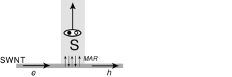
Note that at the two locations (right and left on Fig. 4) where the tube meets the superconductor, normal scattering is likely to occur because bending the nanotubes generates topological defects in the latter [23, 31]. Paradoxically, this scattering is necessary in order to break translational invariance, so that the electron incoming from the left can indeed be “Andreev-transmitted” into a hole on the right (an not be Andreev-reflected on the left). Alternatively, the superconducting material could be evaporated on top of the nanotube.
V Entanglement diagnosis and scattering theory
A “Wavepacket reduction” with selective filters
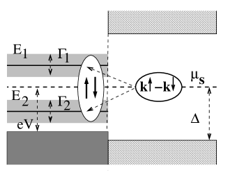
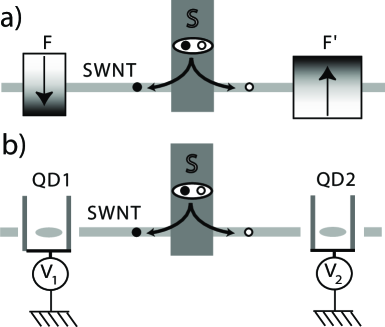
The positive correlations of section III were due to the splitting of a Cooper pair, with the two constituent electrons being redistributed among the two arms of the nanotube. Entanglement will occur if a Cooper pair is prohibited to enter a given lead as a whole. In Fig. 5, two specific setups which implement a selective filtering of the correlated electrons are proposed: a) using two ferromagnetic metal pads (with magnetizations in opposite directions) in each lead (Fig. 5a) which effectively block propagation of electrons bearing the opposite spin, b) exploiting the difference in kinetic energies of electron and hole quasiparticles and thus positioning either a single gate controlling the energy of intramolecular quantum dots which have been defined either by intramolecular scatterers [36, 37] or by defining set of gates on the leads (Fig. 5b) that will act as a Fabry-Perot-like energy filters.
The extension of the setup proposed in Ref. [7] to two–channel leads is straightforward. With filters, this forked superconductor geometry is a two terminal one, where electrons with a given spin from lead are converted into holes with an opposite spin in lead . The noise correlations between normal leads and exactly corresponds to the noise in one of the leads:
| (9) | |||||
with the applied bias. are “transmission eigenvalues” of the matrix , which correspond to the Andreev reflection probabilities in the so-called eigen-channel representation [18]. For ferromagnetic filters (SN-FF) with the spin in F1(2) pointing up (down) and (the propagation of other states is blocked). For the setup selecting quasiparticles and quasi–holes in leads N1 and N2 via Fabry-Perot type filters, we have to sum over spins with and . The decomposition of Eq. (9) leading to the scattering matrix eigenvalues has been exploited recently in the analysis of multiple Andreev reflection phenomenon in atomic point contacts created with break junctions, thus uncovering the “mesoscopic code” of such devices [39]. The spin current which flows in one branch is thus perfectly correlated to the opposite spin current in the other lead [38]: .
The wave function which describes entangled states in this two channel, two lead device is now written for the two types of filters, in the eigen-channel representation [18]. For spin filters,
| (11) | |||||
where the first (second) argument in refers to the quasi-particle state in lead 1 (2) evaluated behind the filters; is the SWNT eigen-channel index and is a spin index; the coefficients and can be tuned by external parameters, e.g., a magnetic field. Note that by projecting the spin degrees of freedom in each lead, the spin entanglement is destroyed. Nevertheless, the energy degrees of freedom are still entangled, and could in principle lead to a measurement of quantum mechanical non locality: a measurement of energy in lead projects the wave function so that the energy has to occur in lead . Such a measurement could be made connecting the device to a set of quantum dots/energy filters. However a direct analogy with Bell–type inequalities for photons with crossed polarizers is not possible here.
On the other hand, the energy filters do preserve spin entanglement:
| (13) | |||||
Note that in principle, the electrons emanating from the energy filters could be analyzed in a similar manner as in Bell type measurements, using now spin filters with variable magnetization orientation as a detection setup. the efficiency of spin filtering by connecting a ferromagnetic electrode on a SWNT has already been pointed out [40], while transport of spin-polarized electrons in a carbon nanotube has been already experimentally observed[41].
B Entanglement detection: Bell inequalities
Strictly speaking, the measurement of perfect noise correlations as illustrated in Eq. (9) only constitutes a proof of charge correlation between the two leads. We now address the correlations of charge and spin. In photon experiments, entanglement is detected in Bell setups, where coincidence measurements count the scattered photons along different polarization directions. Here we exploit the analogy with this bosonic system by specifying energy filters only. As the spin entanglement is preserved by such filters, this opens up the possibility for making current measurements with polarized contacts of various orientation. Indeed, the respective polarization orientation of a set of ferromagnetic nano-electrodes can be controlled by an external magnetic field because the magnetization reversal is a function of the size of the electrode.
Another point that differs from the photon experiments is that transport (average current, or noise correlations averaged over time) are typically measured, while it is possible to detect photons one by one. Nevertheless, at long times, noise correlations at zero frequency can be connected to number counting correlations. Let denote the number of electrons detected in a time interval and the corresponding current noise correlations spectrum . In the limit of large times, the number correlator associated with two different leads reads:
| (14) |
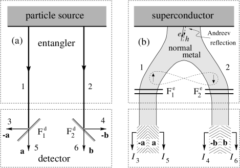
Here, “large” times mean that , where is the lower threshold frequency for noise, and is the upper frequency associated either with the voltage or with the energy width of the filters. It is then possible to transcribe the Bell inequalities expressed usually as correlators of numbers of particles [42] in terms of noise correlators. Care must be taken so that the contribution of the reducible products can be safely neglected. This can be achieved by reducing the transparency of the S-SWNT interface. Here we only mention the main result of Ref. [42]. The typical geometry for testing Bell inequalities, given a source of particles, is depicted in Fig. 6a. The condensed matter implementation which exploits the filters described in the previous sections appears in Fig. 6b. Here it is argued that the measurement of time dependent currents in the different leads of this device, and the subsequent computation of the cross correlation functions, can lead to a Bell inequality test. On general grounds, these noise correlations with arbitrary polarizations in leads and have two contributions:
| (15) |
where, denotes the angle between the magnetization of leads and . is the noise power in the special situation where the orientations of the two ferromagnets are antiparallel (parallel). Let us assume that the energy width of the filters is given by The Bell inequality can be expressed in terms of these two quantities
| (16) |
However, if the only transfer process at the boundary is Andreev reflection (no quasiparticle transmission between the two leads) , so that the Bell inequality is maximally violated. Note that the presence of propagating modes in each arm, and possible channel mixing, does not spoil the detection, because all the quantities are summed over channel numbers. The result of Eq. (16) confirms that a rigorous test for entanglement can be reached within a scattering approach.
Order of estimates for the current and the noise correlations are obtained with the assumption that the Andreev cross-reflection probability is denoted . Neglecting the angle dependence of the filters, and assuming that electron transmission from the superconductor, then through one of the filter is sequential, gives the current estimate . Using the Schottky formula this yields:
| (17) |
Requiring that the reducible number correlator be negligible compared to the irreducible correlator (the one connected to the noise) thus yields, together with and Eq. (14) :
| (18) |
This means that strictly speaking, if a Bell test is to be performed on this electronic subsystem, the acquisition time, or measurement time, is bounded from above. Note that this is no different from the situation with quantum optics [43], in which photons are detected by coincidence counting. In order to probe entanglement, one needs to distinguish between the two photons of an entangled pair generated by parametric down conversion, and two photons which belong to two distinct pairs, which are uncorrelated. In our solid state setting, this would limit our approach to poorly transmitting Andreev interfaces, or alternatively to extremely selective energy filters. Note however that once the assumption is satisfied, the final expression which is to be checked, Eq. (16), contains only zero frequency noise correlators, and is independent on this acquisition time.
The cross–correlation geometry depicted in Fig. 6 may be difficult to implement in experiments, as ideally electrons with both spin orientations are to be collected in the “double” leads. Other experimental geometries with two leads, based on the violation of Clauser–Horne inequalities [44] (a variant of Bell inequalities) can possibly be implemented in a more straightforward manner as each lead is attached to a single ferromagnet.
VI Single electron picture vs. Luttinger liquid picture
We now enquire how the transport properties of the S-SWNT device can be modified if the nanotube is considered to be a strongly correlated one dimensional system. Close to their Fermi level, metallic (armchair) nanotubes have an energy spectrum which can be approximated by two “crosses”, corresponding to two one–dimensional modes. In the presence of Coulomb interactions, from a theoretical point of view the system can be considered as two Luttinger liquids with total (relative) charge (spin) degrees of freedom [45]. Interaction parameters () characterize the strength of the Coulomb interaction in these sectors: for time reversal symmetric situations, the spin interaction parameters (), while in the absence of Coulomb interactions, . Repulsive electron interactions correspond to . Except for tunneling density of states measurements, there exist little data pointing out to Luttinger liquid behavior when charge propagates along the nanotube. Preliminary two-terminal transport measurements on suspended nanotubes with embedded contacts have recently been performed [46]. According to this work, the low shot noise level cannot be fully understood with a single electron picture. Here, there are two fundamental aspects of Luttinger liquid physics which could influence transport in the S-SWNT device.
First, consider the propagation of charge along the nanotube. Does it remain a “good” wave guide in the presence of interactions ? According to tunneling density of states measurements [16], the Luttinger interaction parameter is “strong” (). It is then predicted [47] that at zero temperature, even the presence of weak impurity scattering can lead to insulating behavior – as shown by renormalization group arguments. Thus the presence of the slightest concentration of impurities could impede electron propagation. Fortunately, at finite temperatures the effective impurity barrier strength is reduced: ( is the bare impurity barrier strength). At “high” enough temperatures, one then recovers a linear current–voltage behavior with a conductance . Note that the higher the temperature, the smaller is the deviation from ideal transmission. Except for renormalization of the free conductance by interactions, one should then expect the single electron picture to hold.
The role of Coulomb interactions can also be minimized if the nanotube is placed on top of a metallic or a doped semiconductor substrate, or when it is located close to a metallic gate. The long range Coulomb interaction in the nanotube is then efficiently screened, increasing the interaction parameter close to its non-interacting value (a thin oxide layer should be planned in order to avoid spurious contacts).
Next consider the injection of electrons in the nanotube. The addition of a single electron does not represent an eigenstate of the nanotube : this is explicit in the vanishing of the density of states at the Fermi level. An electron is decomposed into pairs of right and left moving chiral excitations with fractional charges [48] associated with each sector (charge/spin and total/relative). Such charges can in principle be detected via the combination of an autocorrelation noise measurement and of a noise cross-correlation measurement [49]. Such pairs of charges moving in opposite directions then have entangled degrees of freedom.
Next, consider the injection of two electrons in the nanotube. For the S-SWNT device without filters, two electrons are expected to break up into two pairs of entangled chiral quasiparticles, which are themselves entangled because they originate from the same Cooper pair. Nevertheless, in the presence of Fermi liquid contacts [50], one expect to recover the essential features of a single electron system which is only correlated by the superconductor only, due to the multiple reflections of the quasiparticles at the contacts.
In the presence of selective energy filters or coherent quantum dots, which select positive and negative energies as measured from the superconductor chemical potential, the situation will at first be similar. Quantum dots can accomodate electrons only. Quasiparticles excitations generated by superconductor injection will recombine into electrons when reaching the dots. However, further propagation past the dots, along the nanotube extremities will happen once again in a 1D correlated electron system. It is well known that Luttinger liquids exhibit the phenomenon of charge–spin separation. Charge excitations do not propagate with the same velocity as spin excitations. Experimental claims for the observation of such separation of charge and spin degrees of freedom have been made recently with semiconductor quantum wires obtained with cleaved edge overgrowth techniques [51]. Provided that no impurities bother the propagation of these excitations it is likely to operate also in the S-SWNT device. If one places ferromagnetic filters further down the extremities, there will then be a time delay between the detection of a charge excitation and the detection of a spin excitations. While these effects could affect the Bell analysis, they can be minimized by reducing the propagation length between the dots and the ferromagnetic filters.
VII Possible Fabrication processes
We are aware that the S-SWNT device together with its in-situ integrated entanglement detector is rather difficult to fabricate. However tremendous progresses have been made in the last few years to make the electrical contact between a SWNTs and a metallic electrode reliable and reproducible. Indeed, the contact resistance can be reproducibly controlled at values close to ideal threshold of [52, 14]. The observation of superconductivity induced by proximity effect in carbon nanotubes [33] confirms that correlated electrons can effectively propagate over mesoscopic lengths in SWNTs. We present here several possible directions that could be followed to succeed in realizing such experiment.
First like in most reported experiments for which a metal-SWNT-metal junction could be achieved with a resistance lying in the 10 k range, the SWNT position could be localized by scanning probe or by transmission electron microscopy. Contacts could be then performed in a second step either by depositing noble metal on top [37, 31, 29, 30] or by bonding the SWNT with a laser pulse [33]. It will then involve multilevel deposition of metallic thin films, using aligned masks made by electron beam lithography.
Other fabrication schemes could be envisioned even if first published results have concluded to an increased contact resistance with respect to the previously described method: they involve the fabrication of the metallic contacts as the first step with a rather clean top surface. One could then proceed to the SWNT deposition. There are three different possibilities for that last step : 1) deposition of ex-situ synthesized SWNT, followed by AFM manipulation [54, 55, 56], 2) deposition of ex-situ synthesized SWNT with self assembly guided by functionalized electrodes [57] 3) direct in-situ growth of SWNT from contacting catalytic electrodes [32]. These two latter methods allow batch processing and avoid any alignment step. Many sample could be performed in parallel which provide a great advantage with respect to all other fabrication schemes that involves time-consuming alignment steps. Ferromagnet pads and/or control gates could be deposited before or after the SWNT contacting step depending on the process. In the light of the experimental achievements of Refs. [23, 31], it is tempting to make a specific suggestion – however realistic – for the Bell inequalities device of section V B.
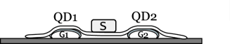
Pursuing the suggestion of section IV, assume that a SWNT has been deposited in good contact with a superconducting island. Now, on each side of the superconductor (Fig. 7), two normal metal islands have also been deposited. Because of the bending of the nanotubes and the resulting barriers due to bending defects, the latter islands allow to define two quantum dots [22,53] which play the role of energy filters. These islands are capacitively coupled to gate electrodes allowing fine tuning of the resonant level in each dot. The resulting device constitutes the Cooper pair splitter with filters. Both ends of the nanotube could therefore be contacted to ferromagnetic leads with varying orientation in order to provide a Bell type test. Finally, note that coincidence measurements for single electron events are likely to be feasible in the near future due to recent improvements in the instrumentation of single electron transistors [53]. An increase of the detection bandwidth of single electron events is still required.
VIII Conclusion
In conclusion, we have proposed a single nanotube which plays the role of a normal superconducting beam splitter. This splitter can be exploited to detect positive (bosonic) correlations in a priori purely Fermionic system. In this first step either metallic of semiconducting nanotubes (with a back-gate) could be used. Moreover, in relation to the ongoing interest in quantum information processing, the addition of filters which select either electron spin or energy could provide a robust scheme for generating entangled pairs electrons at the boundary of a superconductor. This second experiment is likely to be successful using semiconductor nanotubes because excessive screening in metallic nanotubes would render the gates less efficient. This nanotube device combines state of the art technology in both metal/superconductor lithography and manipulation/growth of carbon nanotubes. Complications associated with the correlated nature of the electron state in the nanotube – the Luttinger liquid – have been addressed qualitatively, and indicate that the working temperature should be chosen large enough to minimize the effect of impurities, but low enough to preserve quantum coherence in the device.
On one hand, it would allow for the first time to perform an EPR experiment on massive particles with fermionic statistics. On the other hand, it could become an useful device for quantum information processing.
Acknowledgements.
G.B.L. and N.C acknowledge support from: the Russian science-support foundation, Russian foundation for basic research (grant N 000216617), Russian ministry of science (”Quantum macrophysics” project), Swiss National Foundation, Netherland foundation for collaboration with Russia. N.C. acknowledges support from agreements between Landau Institute and Ecole Normale Supérieure de Paris.REFERENCES
- [1]
- [2] Quantum Computation and Quantum Information, ed. M.A. Nielsen, I.L. Chuang, (Cambridge university press, 2000); The Physics of Quantum Information, D. Bouwmeester, A. Ekert and A. Zeilinger (Springer-Verlag, Berlin, 2000).
- [3] A. Ekert, Phys. Rev. Lett. 67, 661 (1991).
- [4] C.H. Bennett et al., Phys. Rev. Lett. 70, 1895 (1993).
- [5] P. Recher, E.V. Sukhorukov, and D. Loss, Phys. Rev. B 63, 165314 (2001).
- [6] P. Recher and D. Loss, cond-mat/0112298.
- [7] G.B. Lesovik, T. Martin and G.Blatter, Eur. Phys. J. B 24, 287 (2001).
- [8] Y. Makhlin, G. Schön and A. Shnirman, Rev. Mod. Phys., 73,357 (2001).
- [9] Y. Nakamura, Yu.A. Pashkin, and J. S. Tsai, Nature (London) 398, 786 (1999) D. Vion, et al., Science, 296, 886 (1999).
- [10] J. Torrès and T. Martin, Europhys. J. B 12, 319 (1999).
- [11] R. Hanbury–Brown and Q. R. Twiss, Nature 177, 27 (1956).
- [12] V.T. Petrashov et al., Phys. Rev. Lett. 70, 347 (1993); ibid. 74, 5268 (1995); A. Dimoulas et al., ibid. 74, 602 (1995); H. Courtois et al., ibid. 76, 130 (1996); F.B. Müller-Allinger et al., ibid. 84, 3161 (2000).
- [13] A. Einstein, B. Podolsky, and N. Rosen, Phys. Rev. 47, 777 (1935).
- [14] W. Liang et al. Nature 411, 665 (2001).
- [15] C. Kane, L. Balents, and M. P. A. Fisher, Phys. Rev. Lett. 79, 5086 (1997).
- [16] M. Bockrath, D. H. Cobden, A. Rinzler, R.E. Smalley, L. Balents, and P. McEuen, Nature 397, 598 (1999).
- [17] R. Landauer, IBM J. Res. Dev. 1, 223 (1957); R. Landauer, Philos. Mag. 21, 863 (1970); Y. Imry, in Directions of Condensed Matter Physics, G. Grinstein and G. Mazenko eds. (World Scientific, 1987); M. Büttiker, Phys. Rev. Lett. 57, 1761 (1986).
- [18] Th. Martin and R. Landauer, Phys. Rev. B 45, 1742 (1992).
- [19] M. Henny et al., Science 284, 296 (1999); W. Oliver, J. Kim, R. Liu and Y. Yamamoto, ibid, 299 (1999); T. Martin and R. Landauer, Phys. Rev. B 45, 1742 (1992); M. Büttiker, Phys. Rev. B 45, 3807 (1992).
- [20] T. Gramespacher and M. Büttiker, Phys. Rev. B 61, 8125 (2000).
- [21] M.J.M. de Jong and C.W.J. Beenakker, Phys. Rev. B 49, 16070 (1994); B.A. Muzykantskii and D.E. Khmelnitskii, ibid. 50, 3982 (1994); M.P. Anantram and S. Datta, ibid. 53, 16 390 (1996); G. Lesovik, T. Martin, and J. Torrès, ibid. 60, 11935 (1999); J. Torrès, T. Martin and G.B. Lesovik, ibid. 63, 134517 (2001).
- [22] G. Siffert and T. Martin (unpublished).
- [23] A. Bezryadin, A.R.M. Verschueren, S.J. Tans, and C. Dekker Phys. Rev. Lett. 80, 4036 (1998).
- [24] A. Bachtold, M. S. Fuhrer, S. Plyasunov, M. Forero, Erik H. Anderson, A. Zettl and Paul L. McEuen, Phys. Rev. Lett. 84, 6082 (2000).
- [25] C.T. White and T.N. Todorov, Nature 393, 240 (1998).
- [26] S. J. Tans, A.R.M. Verschueren and C. Dekker Nature 393, 49 (1998).
- [27] Xiaolei Liu et al. Appl. Phys. Lett. 79, 3329, (2001).
- [28] Jing Kong, Jien Cao, Hongjie Dai and Erik Anderson Appl. Phys. Lett. 80, 73 (2002).
- [29] A.Bachtold, P. Hadley, T.Nakanishi,and C.Dekker Science 294, 1319 (2001).
- [30] V. Derycke, R. Martel, J. Appenzeller, Ph. Avouris, Nano Lett., published Online 26 August 2001.
- [31] H. W. Ch. Postma, T. Teepen, Z. Yao, M. Grifoni and C. Dekker, Science 293, 76, (2001). D. Bozovic et al., Appl. Phys. Lett. 78, 3693, (2001).
- [32] L. Marty et al., Microelec. Engin., 61 in press (2002).
- [33] A. Yu. Kasumov et al, Science 284, 1508 (1999).
- [34] C. Bena, S. Vishveshwara, L. Balents and M. P. A. Fisher, cond-mat/0202102.
- [35] M. S. Choi, C. Bruder and D. Loss, Phys. Rev. B62, 13569 (2000); G. Falci, D. Feinberg and F. W. J. Hekking, Europhys. Lett. 54, 255 (2001).
- [36] L. Chico, M. P. L. Sancho, M. C. Munõz, Phys. Rev. Lett. 81, 1278 (1998).
- [37] M. Bockrath et al., Science 291, 283 (2001).
- [38] G. Deutscher and D. Feinberg, Appl. Phys. Lett. 76, 487 (2000).
- [39] M. F. Goffman, R. Cron, A. Levy-Yeyati, P; Joyez, M. H. Devoret, D. Esteve, and C.Urbina, Phys. Rev. Lett. 85, 170 (2000); R. Cron, M. F. Goffman, D. Esteve, and C. Urbina, ibid. 86, 4104 (2001).
- [40] D. Orgassa et al., Nanotech., 12, 281, (2001).
- [41] K.Tsukagoshi, B. W. Alphenaar and H. Ago, Nature 401, 572-574 (1999).
- [42] N. Chtchelkatchev, G. Blatter, G. B. Lesovik and T. Martin, cond-mat/0112094.
- [43] A. Aspect, J. Dalibard, and G. Roger, Phys. Rev. Lett. 49, 1804 (1982); Z.Y. Ou and L. Mandel, Phys. Rev. Lett. 61, 50 (1988); Y.H. Shih and C.O. Alley, Phys. Rev. Lett. 61, 2921 (1988); G. Weihs, T. Jennewein, C. Simon , Phys. Rev. Lett. 81, 5039 (1998); A. Aspect, Nature 398, 189 (1999).
- [44] J.F. Clauser and M.A. Horne, Phys. Rev. D 10, 526 (1974).
- [45] R. Egger, A. Bachtold, M. Fuhrer, M. Bockrath, D. Cobden, and P. McEuen, in Interacting Electrons in Nanostructures, edited by R. Haug and H. Schoeller (Springer, 2001).
- [46] P.-E. Roche, M. Kociak, S. Guéron, A. Kasumov, B. Reulet, and H. Bouchiat, Eur. Phys. J. B 28, 217 (2002).
- [47] C. L. Kane and M.P.A. Fisher, Phys. Rev. Lett. 68, 1220 (1992); Phys. Rev. B 46, 15233 (1992).
- [48] K.-V. Pham, M. Gabay, and P. Lederer, Phys. Rev. B 61, 16397 (2000); K.-I. Imura, K.-V. Pham, P. Lederer, and F. Piéchon, Phys. Rev. B 66, 035313 (2002).
- [49] A. Crepieux, R. Guyon, P. Devillard, and T. Martin, cond-mat/0209517.
- [50] I. Safi and H. Schulz, Phys. Rev. B 52, 17040 (1995); D. Maslov and M. Stone, Phys. Rev. B 52, 5539 (1995); V.V. Ponomarenko, Phys. Rev. B 52, 8666 (1995).
- [51] Y. Tserkovnyak, B. I. Halperin, O. M. Auslaender, and A. Yacoby, Phys. Rev. Lett. 89, 136805 (2002).
- [52] B. Reulet et al., Phys. Rev. Lett. 85, 2829 (2000). M. Kociak et al., Phys. Rev. Lett. 86, 2416 (2001);
- [53] R. J. Schoelkopf, P. Wahlgren, A. A. Kozhevnikov, P. Delsing, D. E. Prober, science 280 1238 (1998); A. Aassime et al., Nanotech. 12, 96,(2001) and refs therein.
- [54] H. Postma, A. Sellmeijer, and C. Dekker Adv. Mat. 12, 1299(2000).
- [55] C. Thelander et al, Appl. Phys. Lett. 79,2106 (2001).
- [56] L. Roschier et al, Appl. Phys. Lett. 75,728 (1999)
- [57] K.H. Choi, et al, Surface Science,462,195 (2000).