Spin-dependent properties of a two-dimensional electron gas with ferromagnetic gates
Abstract
A theoretical prediction of the spin-dependent electron self-energy and in-plane transport of a two-dimensional electron gas in proximity with a ferromagnetic gate is presented. The application of the predicted spin-dependent properties is illustrated by the proposal of a device configuration with two neighboring ferromagnetic gates which produces a magnetoresistance effect on the channel current generated by nonmagnetic source and drain contacts. Specific results are shown for a silicon inversion layer with iron gates. The gate leakage current is found to be beneficial to the spin effects.
The generation, control, and measurement of electron spin polarization are the essential ingredients of spintronics. The celebrated giant magnetoresistance effect in metallic multilayers has lead to the realization of remarkable non-volatile magnetic random access memories. A great deal of interest is presently focused on semiconductor spintronics because of the potentially appealing nonlinear functionalities offered by semiconductors review . One particularly relevant system is that with planar confined carriers whose density can be controlled by a gate. Datta and Das Datta proposed a spintronics device consisting of a gated two-dimensional electron gas (2DEG) with magnetic source and drain contacts. The spin valve behavior of the Datta and Das proposal depends on the orientation of the magnetization in the source and drain contacts and is modulated by the Rashba spin-orbit effect rashba induced by the gate. Much recent progress in spin injection review and control of spin-orbit interaction nitta has been made towards the goal of an eventual demonstration of the Datta and Das device.
In this letter, we investigate the spin-dependence of the energies and lifetimes of a two-dimensional electron gas where the ferromagnetic elements are the gates, while the source and drain are nonmagnetic contacts. The spin-dependence of the electronic transport arises out of the proximity to the ferromagnetic gates, in stark contrast to the injection of spin-polarized electrons from the ferromagnetic source. Recent experiments FMimprinting ; FMcoherence have shown that large spontaneous spin polarization can be achieved in an optically excited semiconductor layer in contact with a ferromagnet . This phenomenon is explained in terms of spin-dependent reflection at the semiconductor/ferromagnet interface imprinting . For quantum confined semiconductor electrons, the proximity effect with the ferromagnet is equivalent to multiple reflections. A required condition is that the interface barrier is sufficiently thin to allow for sizeable wave-function coupling. This is analogous to the proximity effect of a metal such as Pd next to Fe ivan . Our scheme avoids the restrictions of the Rashba effect, namely narrow gap semiconductors (for large spin-orbit coupling) and one-dimensional channels (to maximize the favorable directions of spin torque). There is a wider range of appropriate systems for our scheme, such as the inversion layer in Metal-Oxide-Semiconductor (MOS) structures, the 2DEG in a modulation doped III-V quantum well, and the InAs accumulation or inversion layers. The paper is structured as follows. We shall discuss (i) the spin-dependent properties of a 2DEG with a single ferromagnetic gate, (ii) a device proposal of a spin valve with two neighboring gates, (iii) model results for a silicon inversion layer with iron gates.
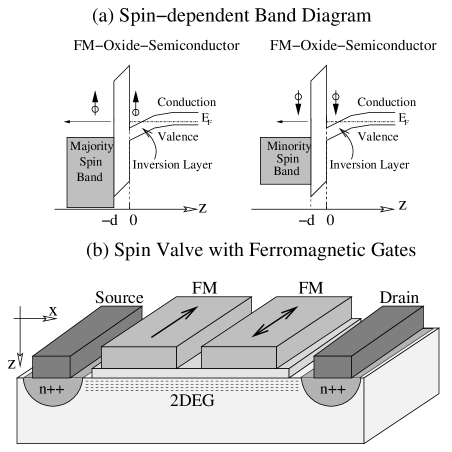
(i) 2DEG with a single ferromagnetic gate
The tunneling coupling
of the electron wave function in the 2DEG to the exchange-split band
states in the metal produces a spin-dependent broadening and shift of the
quantized electron energy in the 2DEG. Namely, we have a complex energy
where () refers to the majority (minority)
spin channel. Note that
describes the escape time of the quasi-bound semiconductor
electrons into the ferromagnet band continuum. Due to the spin-dependent
self-energy, the in-plane transport of the 2DEG is described by the
spin-dependent conductance whose expression is
| (1) |
where is the ordinary spin-independent Drude scattering time, the in-plane effective mass and the spin-dependent density of the 2DEG due to the spin splitting . However, this is not the only aspect of the problem, because a fraction of the channel current is leaked into the gate (implying that drain and source currents are different). The spin-dependent leakage probabilities for non-equilibrium electrons injected into the channel are governed by the transit times where is the length of the gate (along the -direction) and are the spin-dependent drift velocities induced by the source-drain bias . Namely,
| (2) |
In the linear regime, the drift velocity is where is the in-plane field due to the source-drain bias and are the spin-dependent mobilities. When the lateral extension of the 2DEG channel is shorter than the spin mean-free path, the majority and minority spin channels can be considered decoupled in the active region between the source and drain contacts. Hence, the spin-dependent drain current will be , i.e., the channel conductance is renormalized by the leakage probability. Note that the shorter the , the smaller are both and . Hence, the leakage current, which ordinarily reduces the channel current, actually enhances the difference between the renormalized resistances of the two spin channels.
(ii) Spin valve with two ferromagnetic gates
The
spin-dependent in-plane transport due to the proximity of a
ferromagnetic gate can be conveniently exploited to design a spin
valve (see Fig. 1b). If two neighboring ferromagnetic gates are used,
the electron current detected at the drain contact will depend on the
relative orientation of the magnetizations of the two gates, giving
rise to the magnetoresistance ratio where and are the total drain currents for parallel and antiparallel magnetizations respectively. For simplificity, we
consider the case where the two ferromagnetic gates are identical and
the effect of the channel region between the two gates on the current
is negligible. The spin-dependent channel current density,
is driven by
the electrochemical potential and is constrained by
the continuity equation accounting for the leakage of current into the
gates. Combining the two equations leads to a second order
differential equation for . The boundary conditions
are (a) () at the edge
of the gate near the nonmagnetic source (drain) contact, (b)
and vary continuously along .
Under the first gate, . Under the second
gate, in parallel configuration, but
in the antiparallel case. We
have solved exactly this equation both for the parallel and antiparallel
configuration. The analytical expression for the magnetoresistance ratio
is quite involved and will be presented in a longer
publication. However, we have verified that a good approximation
is given by
| (3) |
This formula is obtained by a circuit diagram of the two spin channels in parallel and by properly combining in series the leakage-renormalized conductances for the two gates.
(iii) Model results for a silicon inversion layer
Here we
present reasonable estimates for a
heterostructure. We consider a free-electron Hamiltonian with two
exchange split spin bands in the ferromagnet slon , an insulator
barrier and the electrostatic confinement potential for the inversion
layer. We will focus on the low temperature regime in which only the
first quantized subband in the inversion layer is filled and the
confining potential can be approximated with a triangular shape
(Fig. 1a). As suggested by the recent literature on
tunneling Si2 ; Si3 , the conservation of the in-plane wave-vector is
relaxed and, hence, a one-dimensional calculation can be carried out.
Within this simplified model, the spin-dependent wave-function
of the quasi-bound electron in the inversion layer can be
written in terms of special Airy functions and .
For (the semiconductor region),
| (4) |
where depends on the electric field in the inversion layer and the semiconductor effective mass . The position represents the turning point. For (the insulator barrier region),
| (5) |
where and is the electric field in the barrier region ( and being the dielectric constants) and is the extrapolated turning point. The quantity is the quantization energy of the inversion layer subband and has to be calculated self-consistently. Finally, for ,
| (6) |
where in terms of , the spin-dependent Fermi wave-vector and , the ferromagnet band mass. The term is the mean-free path in the ferromagnet. The coefficients , , , are determined by the usual boundary conditions at the interfaces and . The resultant secular equation for has a complex solution, yielding the spin-dependent complex energy in the inversion layer.
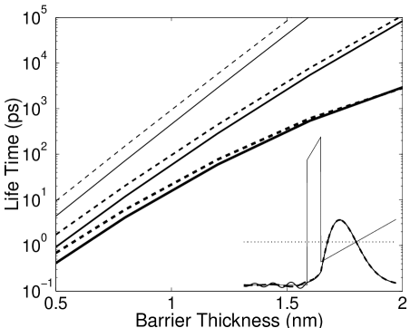
Fig. 2 depicts the majority and minority spin life times (solid lines) and (dashed lines) as functions of the oxide thickness. The ultrathin range of the oxide thickness and the oxide electron effective mass are based on the recent measurements of electron tunneling across the silicon-based MOS junction Situnneling ; Si2 ; Si3 . The spin-dependent life time decreases exponentially with decreasing barrier thickness. The ratio of the times for two spins, , is dependent on the parameters of the ferromagnetic junction and can exceed a factor of 2. An increase of the electric field in the oxide (via the gate voltage) dramatically shorten the lifetimes, approaching the picosecond range. The oxide electric fields from the top to the bottom curves are 2, 7, and 12 V/cm (the highest value approaches the dielectric breakdown). These results show a significant spin-dependence of the channel mobility for ultrathin oxide thickness. The spin splitting (not shown) is comparable to the energy broadening and is about 0.3 meV when the lifetime is of the order 1 ps. Thus, for this specific system, the spin splitting can be disregarded because it is much smaller than the Fermi energy of the 2DEG. The leakage probability depends also on the drift velocity according to Eq. (2). For a gate length m, in-plane field m and Drude scattering time ps, the transit time in the gated region is ps. This means that when the spin-dependent lifetimes are ps and ps, the leakage probabilities are and . With these parameters, we get a magnetoresistance ratio . A decrease of the drift velocity (through a decrease of the source-drain bias) will make the leakage of the channel current more severe (thus reducing the drain current), although it will increase according to Eq. (3).
In summary, we have predicted the spin-dependent properties of a 2DEG system due to the proximity of ferromagnetic gates, showing the potential spintronics applications of this kind of configuration.
Acknowledgements.
This work is supported by DARPA/ONR N0014-99-1-1096 and NSF DMR 0099572. CC is also grateful to the Swiss National Science Foundation for additional support. JPM acknowledges support by the California Institute for Telecommunications and Information Technology. We thank Edward Yu, Daniel Schaadt, and Ivan Schuller for helpful discussions.References
- (1) S. A. Wolf, D. D. Awschalom, R. A. Buhrman, J. M. Daughton, S. von Molnar, M. L. Roukes, A. Y. Chtchelkanova, D. M. Treger, Science 294 1488 (2001).
- (2) S. Datta and B. Das, Appl. Phys. Lett. 56, 665 (1990).
- (3) Yu. A. Bychkov and E. I. Rashba, Sov. Phys. JETP Lett. 39, 78 (1984).
- (4) J. Nitta, T. Akazaki, H. Takayanagi, T. Enoki, Phys. Rev. Lett. 78, 1335 (1997).
- (5) R. K. Kawakami, Y. Kato, M. Hanson, I. Malajovich, J. M. Stephens, E. Johnston-Halperin, G. Salis, A. C. Gossard, D. D. Awschalom, Science 294, 131 (2001).
- (6) R.J. Epstein, I. Malajovich, R. K. Kawakami, Y. Chye, M. Hanson, P. M. Petroff, A. C. Gossard, and D. D. Awschalom, Phys. Rev. B 65, 121202 (2002).
- (7) C. Ciuti, J. P. McGuire, and L. J. Sham, Phys. Rev. Lett. 89, 156601 (2002).
- (8) An up-to-date review is given by J. J. Akerman, I. Guedes, C. Leighton, M. Grimsditch, I. K. Schuller , Phys. Rev. B 65, 104432 (2002).
- (9) J. C. Slonczewski, Phys. Rev. B 39, 6995 (1989).
- (10) S. H. Lo, D. A. Buchanan, Y. Taur, W. Wang, IEEE Electron Device Letters 18, 209 (1997).
- (11) W. K. Shih, E. X. Wang, S. Jallepalli, F. Leon, C. M. Maziar, A. F. Taschjr, Solid-State Electronics 42, 997 (1998).
- (12) B. Brar, G. D. Wilk, and A. C. Seabaugh, Appl. Phys. Lett. 69, 2728 (1996).
- (13) J. Hong and D. L. Mills, Phys. Rev. B 62, 5589 (2000).