Fabrication of Nano-Scale Gaps in Integrated Circuits
Abstract
Nano-size objects like metal clusters present an ideal system for the study of quantum phenomena and for constructing practical quantum devices. Integrating these small objects in a macroscopic circuit is, however, a difficult task. So far the nanoparticles have been contacted and addressed by highly sophisticated techniques which are not suitable for large scale integration in macroscopic circuits. We present an optical lithography method that allows for the fabrication of a network of electrodes which are separated by gaps of controlled nanometer size. The main idea is to control the gap size with subnanometer precision using a structure grown by molecular beam epitaxy.
Recently, there is growing interest in the study of the electrical properties of nano-size objects. In these small scale structures the energy associated with size quantization and the Coulomb energy are considerably enhanced and can exceed the thermal energy at room temperature. Therefore, such systems are ideal for studying quantum phenomena and for constructing practical quantum devices. The single-electron transistor (SET) has emerged as an important experimental platform in both aspects. It consists of a nano-size metal island which is connected through two tunnel barriers to the leads[1]. The SET also presents most of the problems that characterize device physics at this length scale: fabrication of macroscopic leads with a nanometer-size gap, definition of a nano-size island, positioning it between the leads and controlling the tunnel barriers with high precision. The fabrication of the leads has proven to be a particularly challenging task. It requires nano-scale resolution for defining the gap, and the ability to integrate the device in a highly connected and complex macroscopic circuit. A variety of solutions have been suggested to this issue, of which the majority are appropriate for contacting only a single device. These include using the tip of a scanning tunnelling microscope for contacting[2], electromigration[3], breaking thin wires [4], or metal deposition on electron-beam defined structures[5, 6, 7]. Other techniques attempted to use a conducting DNA-based network[8] to solve the connectivity issue. Recently logic circuits with carbon nanotube have been reported[9].
In this paper we present a method that allows us to fabricate a network of electrodes that are separated by gaps of controlled nanometer size using conventional optical lithography. The gap size is determined by the thickness of a molecular beam epitaxy (MBE) grown layer embedded in a sandwich structure. This layer is selectively etched and after metal evaporation a gap is formed exactly where the layer was removed. Controlled positioning of the nanoparticles between the electrodes is done by electrostatic trapping[7]. We show that the device exhibits clear Coulomb blockade (CB) characteristics in the transport measurements and can function as an SET.
The sample fabrication is illustrated in Fig. 1 (a)-(d). A quantum-well (QW) structure is grown on a GaAs substrate by MBE. The thickness of the two undoped AlGaAs layers above and below the QW are 200 nm and 100 nm, respectively. The thickness of the embedded GaAs layer is varied between 5 to 10 nm in various samples. In the first step, 200 nm high mesa structures are defined by optical lithography and a standard wet-etching process such that the GaAs layer is exposed on the side of the mesa (Fig. 1 (a)). Next, the pattern of the electrodes is defined by optical lithography. On the exposed areas a few tens of nanometers of the GaAs layer (from the side) are removed by selective wet-etching [10] using citric acid and H2O2 (5:1), as shown in Fig. 1 (b). The selectivity of the etching between GaAs and AlGaAs is nominally 100:1, hence the width of the etched layer is the QW width. The electrodes are fabricated by thermally evaporating a thin film (5 to 15 nm) of PdAu from a direction perpendicular to the plane of the wafer surface such that a gap is formed exactly where the GaAs was removed (Fig. 1(c)). The size of the gap is determined by the crystal structure (which can be controlled with subnanometer precision), surface roughness of the etched AlGaAs/GaAs interface due to the selective etching (less than one nanometer for short etching times), and by the metal evaporation which can be controlled on the nm scale. We manage to fabricate gaps which are less than 5 nm wide and estimate the minimum gap size that can be achieved by our method to be about one to two nanometers. An important advantage of this method is that since the mesa structure and the electrode pattern are defined by optical lithography, it allows the simultaneous fabrication of many electrodes separated by nano-size gaps on the wafer surface (see illustration in Fig. 1 (f)).
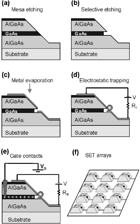
To position the nanoparticles between the electrodes we use the method of electrostatic trapping [7]: the electrodes are immersed in an aqueous or organic solution of Au clusters. The Au clusters can be chemically fabricated with controlled size in the range of 1 to 100 nm diameter[11]. By applying a voltage between the electrodes a dipole moment is induced in the Au cluster and it is attracted to the point of strongest electric field, i.e. the gap, by dipole-dipole interaction. A series resistance, = 1 G, is integrated in the circuit such that when trapping occurs the voltage drops on that resistor and the device cannot trap more clusters. In this way only a single cluster is trapped in the gap. The setup is sketched in Fig. 1 (d). For trapping, we apply an AC voltage of 8 V at 50 kHz for a few seconds. AC voltage is used to increase the impedance of the liquid solvent and to be able to trap also charged particles. After trapping, the liquid is blown off with .
In order to form tunnel barriers between the electrodes and the clusters, the electrodes can be covered with thiol molecules before the trapping[3, 5]. However, we find that if the cluster diameter is only slightly larger than the gap, a tunnel barrier can exist even for uncoated electrodes. This tunnel barrier could arise from organic molecules on the cluster surface that stabilize the Au clusters, or from contamination on the electrodes formed during the trapping process. We note, however, that the strength of this barrier is reasonably reproducible as evidenced by transport measurements. The geometry sketched in Fig. 1 (d) suggests that the contact of the trapped cluster to the lower electrode is better than to the upper one. This asymmetry in the contacts should lead to different tunnel resistances, which is indeed the case as we will see below.
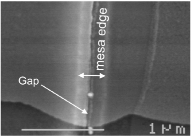
A scanning electron microscope (SEM) image of a single trapped cluster between two metal electrodes is displayed in Fig. 2. In the center of the image we see the mesa edge, with the mesa plateau to the left, and the etched grove separating the electrodes in the vertical direction. The trapped cluster is seen below the center of the image. Two more clusters, which do not bridge the gap, can be observed at the right side of the scale bar. The gap size is slightly larger than 10 nm and the width of the electrodes is a few microns each. To enhance the visibility of the trapped cluster, clusters having a relatively large diameter of 60 nm are displayed.
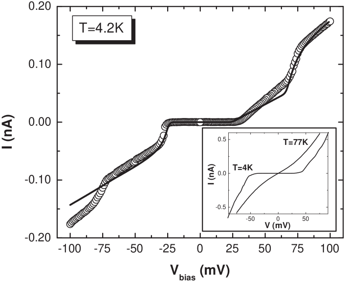
Figure 3 shows an curve measured on a trapped Au clusters with 10 nm diameter at 4.2 K. A clear CB behavior can be observed up to mV. For larger voltages, mV, we observe a strong asymmetry in the curve with respect to positive and negative voltage. For positive bias voltage we find a linear rise in current in the range of 25 mV65 mV, whereas for negative bias we observe a step-like feature at mV, which then saturates in a linear slope. This asymmetric behavior has been discussed by Hanna and Tinkham [12] assuming different tunnel resistances to the electrodes, i.e. . They distinguished four different cases in a phase diagram, each with a qualitatively different onset in conduction. Here and are the capacitances of the trapped cluster to the electrodes and is the residual fractional charge on the cluster. The solid line displayed in Fig. 3 corresponds to the case of and . In order to fit our data [13, 14], we used M, M (which satisfies very well the assumption of ,) and for the capacitances x F, and a stray capacitance to the electrodes of x F. The inset in Fig. 3 shows transport measurements of another sample at different temperatures, where a Au cluster with a diameter of 10 nm was trapped. At K we find the CB region to be slightly larger than in the previous sample. Clearly, also at higher temperatures K a non-linear behavior in the curve can be observed. Measuring the curve of a certain device at different times after the cooling reveals the abrupt occurrence of changes in the characteristics of the conduction onset and slight changes in the size of the Coulomb blockade region. This behavior was also observed by Klein and coworkers [5] and was attributed to changes in the local charge distribution in the vicinity of the cluster. Repeated warming and cooling of the device leads to similar effects.
An important question is how to apply a gate voltage to the trapped cluster in order to get true transistor functionality. This is not trivial and to the best of our knowledge, so far no gated device using metal clusters of nanometer size has been realized. The major problem is the screening of the gate voltage by the comparatively large electrodes in close vicinity to the small cluster. Our design provides a very elegant method to position a gate electrode only a few tens of nanometers away from the cluster. As illustrated in Fig. 1 (e), the GaAs layer, which has been used for the selective etching, can also be heavily doped during the MBE growth and then used as a gate. The great advantage of this method is that due to the mesa design, each cluster can be gated individually. This would allow large scale integration of SETs with true transistor functionality on semiconductor surfaces by optical lithography (Fig. 1 (f)), especially if the series resistor is also integrated in the electric circuit on the wafer. This would enable simultaneous trapping on a large number of devices. Another approach to position a gate electrode in very close proximity to the cluster is to grow the lower AlGaAs layer only a few tens of nanometers thick and to use a n-doped GaAs substrate. In this design the substrate could serve as a gate, however, this setup would not allow the individual gating of each cluster. Experiments to realize a gated structure are in progress and will be reported elsewhere.
In conclusion we presented a fabrication method to define compatible contacts to nanosize objects by optical lithography and selective etching. In transport measurements at low temperatures we demonstrated Coulomb blockade behavior. In order to operate the nanoclusters as SETs we proposed a gate design that allows large scale integration of such devices on semiconductor surfaces.
We want to thank Diana Mahalu for helpful discussions and her assistance in the early stages of this work. The research of R. K. was supported by the ”Fritz Thyssen Stiftung” and the European Commission under contract HPRI-CT-1999-00069. This work was partially supported by a grant from the Israel Science Foundation to J. S.
REFERENCES
- [1] T. A. Fulton and G. J. Dolan, Phys. Rev. Lett. 59, 109 (1987).
- [2] D. Porath, Y. Levi, M. Tarabiah, and O. Millo, Phys. Rev. B 56, 9829 (1997).
- [3] H. Park et al., Appl. Phys. Lett. 75, 301 (1999).
- [4] M. A. Reed et al., Science 278, 278 (1997).
- [5] D. L. Klein et al., Appl. Phys. Lett. 68, 2574 (1996).
- [6] D. Porath, A. Bezryadin, S. de Vries, and C. Dekker, Nature 403, 635 (2000).
- [7] A. Bezryadin, C. Dekker, and G. Schmid, Appl. Phys. Lett. 71, 1273 (1997).
- [8] E. Braun, Y. Eichen, U. Sivan, and G. Ben-Yoseph, Nature 391, 775 (1998).
- [9] A. Bachtold, P. Hadley, T. Nakanishi, and C. Dekker, Science 294, 1317 (2001).
- [10] G. C. de Salvo, W. F. Tseng, and J. Comas, J. Electrochem. Soc. 139, 831 (1992).
- [11] G. Schmid, Clusters and Colloids (VCH, New York, 1994).
- [12] A. E. Hanna and M. Tinkham, Phys. Rev. B 44, 5919 (1991).
- [13] A. Korotkov and Y. Nazarov, Physica B 173, 217 (1991).
- [14] A. Korotkov, http://qt.tn.tudelft.nl/CHARGE/ .