Nonlinear behavior in the Thermopower of Doped Carbon Nanotubes
Due to Strong, Localized States
Abstract
The temperature dependent thermoelectric power (TEP) of boron and nitrogen doped multi-walled carbon nanotube mats has been measured showing that such dopants can be used to modify the majority conduction from p-type to n-type. The TEP of boron doped nanotubes is positive, indicating hole-like carriers. In contrast, the nitrogen doped material exhibits negative TEP over the same temperature range, suggesting electron-like conduction. Therefore, the TEP distinct nonlinearites are primarily due to the formation of donor and acceptor states in the B- and N- doped materials. The sharply varying density of states used in our model can be directly correlated to the scanning tunneling spectroscopy studies of these materials.
pacs:
65.80+n, 61.46+w, 73.63.Fg, 81.07.DeInterest in the electrical transport properties of both single-walled (SWNT) and multi-walled (MWNT) carbon nanotubes stems primarily from anticipated applications of these low-dimensional materials in nanoelectronics dekker . One expects metallic conduits along with heterojunctions, formed from nanomaterials with different carriers (electrons vs. holes), to be necessary. These would play an analogous role to ’bulk’ doped Si devices and metal interconnect lines. However, the direct substitutional doping of carbon nanotubes has proven to be quite difficult. Their low-dimensional structure does not provide an energetically favorable environment for most impurity atoms. Fortunately, there are two promising exceptions, boron red and nitrogen terrones , both of which seem able to reside within the carbon lattice.
In this Letter we report on the effect of donor and acceptor states on the thermoelectric power (TEP) of boron doped and nitrogen doped nanotube mats. TEP is an important and sensitive test of the carrier sign of any material. Because the TEP is a zero current transport coefficient, it can probe the intrinsic conduction properties of individual nanotubes while being less influenced by randomly entangled morphologies and imperfections of the measured mats as compared to standard conductivity measurements kaiser01 . For example, intrinsic-metallic properties were well demonstrated with the TEP of conducting polymer films exhibiting randomly entangled fibrillar morphologies. However, in these systems, the electrical conductivity always showed a semiconducting temperature dependence due to interfibrillar junction resistances park80 . Generally, SWNT and MWNT randomly orientated mats show a positive and moderately large thermoelectric power (TEP) over the temperature range of 0 to 300 K, with temperature dependencies that approach zero as T0 bax . However, earlier studies have shown that ”doping” the SWNT mats by intercalating alkali metals into the nanotube bundles could give rise to significantly different thermoelectric properties grig . Likewise, more recent work has demonstrated an extreme sensitivity of the thermoelectric properties of SWNT mats to oxygen contamination (or doping) brad . In fact, this exposure to various atmospheres has become a central issue in understanding thermoelectric measurements in SWNT systems. In both cases, changes in the sign or magnitude of the TEP arise from modifications of the density of states near the Fermi level of the semiconducting tubes contained in the mat, and relatively little effect is attributed to dopant interactions with the metallic tubes in the sample. Furthermore, these dopants were not included within the lattice structure of the carbon nanotubes, but rather they were attached to the outside of the cylindrical shell grig . Thus, they represent something other than intrinsic behavior to this material.
The behavior of the TEP in multi-walled mats is likely to be somewhat different from that of SWNT mats bax . This is because in SWNT mats the microstructure is composed of an assortment of semiconductors and metals, while in the MWNT mats, the tubes are all semi-metals and small band-gap semiconductors. In fact, many models treat the materials surprisingly the same with a great deal of success model . The theoretical approach to MWNT mats adopted by most researchers has been the inclusion of parallel metallic and semiconducting conduction paths each broken by tube-tube contact barriers. While this view is clearly adequate for understanding pure mats of MWNTs, modifications are required when addressing the TEP of doped materials. Here we demonstrate that while the rather large positive TEP for pure materials might arise from the random orientation of contact barriers within the mat and pure semiconducting pathways, B-doped nanotube mats exhibit a positive TEP, with a more metallic-like thermopower, and derived entirely from the sign of the carrier in the isolated nanotubes. Further, N-doped nanotube mats exhibit a metallic negative TEP that is again a reflection of the isolated nanotube’s behavior. Thus, control over the nature of the carrier in MWNTs has been achieved in direct analogy to bulk semiconductors.
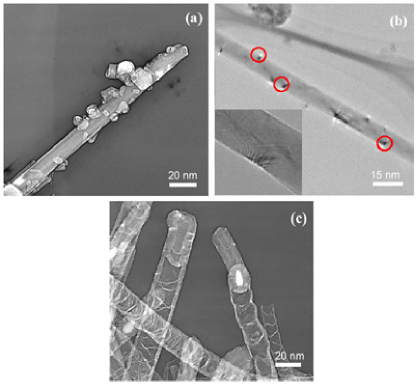
For these studies, a variety of growth and processing techniques had to be used to prepare the pure and doped materials. The pure carbon nanotubes were arc grown using methods described in detail elsewhere ebb . Transmission electron microscopy (TEM) showed a diameter distribution to be centered around 20 nm with tubes as small as 3 nm and as large as 40 nm. Tube lengths were typically 1-3 m and the primary impurities were carbonaceous materials and polyhedral particles, as shown in Fig. 1a. B-doped MWNTs were also grown using arc methods as described in the literature red94 . TEM characterization showed these materials to have typical tube diameters of 20 nm with a range of 5 nm to 40 nm. Selected area diffraction (SAD) confirms that these tubes possess a predominantly zig-zag chirality blase . Previously, tunneling microscopy and spectroscopy, coupled with electron energy loss spectroscopy (EELS), has been used to demonstrate that the boron is incorporated into the lattice as islands of BC3 carroll . A visual indication of these islands could be attributed to the presence of strained regions within the tubes (Fig. 1b dark contrast regions). The impurities in the growth materials were found to be polyhedral particles and small concentrations of amorphous carbon. No catalysts are used in the growth of either of the arc-produced materials.
Finally, the N-doped materials were grown using catalytic decomposition of melamine-ferrocene mixtures terrones . This technique has only been developed recently and the tubes are well formed with a typical diameter of around 20 nm. Our CVD tubes exhibit only small amounts of polyhdra particles and amorphous material. However, much of the material had encapsulated Fe cores at the very tip of the nanotubes that typically would extend 20 - 30 nm in length as seen in Fig. 1c. All of the micrographs in Fig. 1 show the materials “as grown” before filtering of the impurities and prior to the preparation of the mats. We note that while there are few conformational differences between the pure and B-doped MWNTs (except chirality), the N-doped materials exhibit a “bamboo - like” tube morphology. The tubular segments within the N-doped material are approximately 100 nm in length. In the mats, the segment length is generally longer than the average distance between tube-tube contacts.
Nanotube mats were produced by suspending each (as grown) material into chloroform and then ultrasonically agitating until the nanotubes were well dispersed. The suspended materials were found to be relatively undamaged, after the extended ultrasonication, using TEM. Each solution was allowed to settle and then was filtered multiple times using 0.4 mm Teflon filters. The remaining solution was composed of nanotubes with little amorphous materials and few polyhedra. Finally a thick film was built-up from each of the materials using a Teflon filter and a polyimide mold (to insure equal dimensions in each case). This resulted in a random packing of nanotubes in a dense mat. The samples were 3 mm x 5 mm x 0.025 mm in size. Several mats of each material were made, and the measurements performed several times on each to insure reproducibility. In order to carry out thermoelectric power measurements, the mat samples were supported on a Teflon substrate and mounted on top of two coppers blocks. Silver paste was used for the electrical contacts. Chromel-Constantan thermocouples were attached to the back of the copper blocks using GE 7031 varnish. Techniques for the TEP measurement of carbon nanotubes are described with more detail in the literature kim .
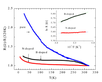
Fig. 2 shows a two-probe measurement of the temperature dependence of R, normalized to 320 K, after degassing in vacuum at 320 K for three days. All three mats exhibited non-metallic behavior over the entire temperature range (dR/dT0). The primary effect of the lattice doping was to reduce the temperature dependence of R. The ratio R20/R320 was reduced from 2.4 in the pristine case to 1.25 and 1.14 in the boron and nitrogen cases, respectively. Similar reductions in the temperature dependence have been reported for I-doped and Cs-doped SWNT mats grig . Fig. 2 inset shows linear fits to an Arrhenius plot of R versus the absolute temperature T. For sufficiently high temperatures, where intrinsic conductivity dominates, one can expect resistivity to follow an Arrhenius type equation of the form:
| (1) |
where Eρ is the activiation energy, is a constant, and k is Boltzman’s constant. For the B-doped mat, the acivation energy (12.2 meV) was found to be larger than the activation energy of the N-doped mats (1.4 meV), but smaller than the activation energy reported for individual B-doped tubes (55-70 meV) wei .
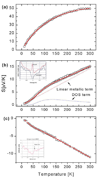
The TEP of the pure mats is shown in Fig. 3a, and the solid line shows the fit using a heterogenous model. Each percolating pathway is assumed to have a randomly oriented set of barriers due to tube-tube contacts, tube defects, etc., It is therefore expected, for such a model, that the TEP will be consistent with the sum of a linear metallic term and an exponentially weighted T1/2 variable range hopping term that reflects the “freezing-out” of semiconducting contributions at low temperatures kaiser99 given by the following equation:
| (2) |
where bT is is the metallic term and q is a constant. However, although this model gives a reasonable fit of the pure data, the TEP is the sum of a very large and un-physical positive metallic term (135 V/K at 300 K), and a correspondingly large negative semiconducting term. The large positive TEP is due in part to oxygen doping of the pure mats. The TEP of the pure MWNT mats in our study was found to decrease by 10.9 V/K at 320 K when the sample was exposed to vacuum for 94 hours. This is in constrast to the boron and nitrogen doped MWNT mats which showed no variation in TEP after similar time exposure to vacuum.
In the case of the doped materials, we suspect nonlinearities are introduced into the linear metallic thermopower by sharply varying and localized states near the fermi level due to the addition of boron or nitrogen into the lattice. Such states have been predicted and subsequently verified experimentally by scanning tunneling spectroscopy (STS) carroll ; czerw . Taking the standard expression for thermopower dugdale :
| (3) |
where is the conductivity, is the chemical potential (assumed to be constant with temperature), (E) the partial conductivity at energy E, and the Fermi function, we approximate the partial conductivity function by a delta function due to the sharply varying density of states near the Fermi level. This gives the following expression for the thermopower kaiser99 :
| (4) |
In this expression, bT is the linear metallic term, q is a constant, and Tp=(E-)/k where E is the energy at which the peak occurs and k is Boltzmann’s constant. As can be seen in Fig. 3b and Fig. 3c, Eq. (4) gives a good fit with E=27 meV and 11 meV for the boron and nitrogen samples, respectively. From the LDOS (Fig. 3b inset), the sign of the TEP for the B-doped materials is not surprising since these nanotubes have strong acceptor states and hole-like conductivity should be expected. In contrast, the N-doped nanotubes show a negative TEP with a similar functional form to that of the B-doped materials. From the large donor state in the LDOS (Fig. 3c inset), it is clear that these materials should be electron rich and thus the sign of the TEP is expected. The shape of the TEP for the doped materials is also very similar to that of the TEP curve for iodine-doped SWNT bundles grig . Since chloroform was used to suspend the tubes during sonication, and chloroform has been shown to result in C-Cl bonds on nanotube surfaces or to react with the amorphous carbon in bundles lee01 , it may be argued that the effects are due to doping by Cl-. However, in the previous study, extremely long sonications and reflux times in the presence of a catalyst were used to form the bonds. It is doubtful that the shorter sonication times in our samples ( 30 min) could result in significant doping by Cl-. Also, the sign of the carrier of the n-doped mats is clearly negative.
In summary, the thermoelectric power in mats of doped MWNT’s reflects the sign of the majority carrier of the individual nanotubes. Further, the behavior of the TEP has been directly correlated with the density of electronic states near Fermi level as determined by STS and gives a positive TEP when acceptor states are present as well as a negative TEP when donor states are present. The TEP of pure MWNT mats has shown some sensitivity to air exposure, while the doped mats are effectively insensitive to “oxygen doping.” The TEP is strongly dominated by the boron and nitrogen doping and the resulting donor and acceptor states near the Fermi level.
The authors gratefully acknowledge support from: KISTEP 98-I-01-04-A-026, MOST (Korea), AFOSR F49620-99-1-0173 (U.S.), DFG (Germany). MT and HT are grateful to CONACYT-Mexico grant W-8001 millennium initiative. NG acknowledges the Royal Society for financial support, and PMA thanks Philip Morris U.S.A. for their financial support.
References
- (1) See for example: C. Dekker, Phys. Today 52, No. 5, 22 (1999).
- (2) P. Redlich, J. Loeffler, P.M. Ajayan, J. Bill, F. Aldinger, and M. Rühle, Chem Phys. Lett.260, 465 (1994).
- (3) M. Terrones et al., Appl. Phys. Lett. 75, 3932 (1999); W.Q. Han et al., Appl. Phys. Lett. 77, 1807 (2000).
- (4) A. B. Kaiser, Adv. Mater. 13, no. 12-13, 927 (2001).
- (5) Y. W. Park, A. J. Heeger, M. A. Druy, and A. G. MacDiarmid, J. Chem. Phys. 73, 946 (1980).
- (6) M. Baxendale, K.G. Lim, and G. A. J. Amaratunga, Phys. Rev. B, 61, 12705 (2000).
- (7) L. Grigorian, G. U. Sumanasekera, A. L. Loper, S. Fang, J.L. Allen, and P.C. Eklund, Phys. Rev. B 58, R4195 (1998).
- (8) K. Bradley, S.-H. Jhi, P. G. Collins, J. Hone, M. L. Cohen, S. G. Louie, and A. Zettl, Phys. Rev. Lett. 85, 4361 (2000).
- (9) Compare for example, the model of Ref. 6 with that of A.B. Kaiser et al., Phys. Rev. B 57, 1418 (1998).
- (10) T. W. Ebbesen and P. M. Ajayan Nature 358, 220 (1992).
- (11) P. Redlich et al., Chem Phys. Lett. 260, 465 (1994).
- (12) X. Blase et al., Phys. Rev. Lett. 83, 5078 (1999).
- (13) D. L. Carroll, P. Redlich, X. Blase, J. C. Charlier, S. Curran, P.M. Ajayan, S. Roth, and M. Rühle, Phys. Rev. Lett. 81, 2332 (1998).
- (14) Y.-W. Park, Synth Met. 45, 173 (1991).
- (15) B. Wei, R. Spolenak, P. K. Redlich, M. Ruhle, and E. Arzt, Appl. Phys. Lett. 74, 3149 (1999).
- (16) A. B. Kaiser, Y. W. Park, G. T. Kim, E. S. Choi, G. Düsberg, and S. Roth, Synth. Met. 103, 2547 (1999).
- (17) R. Czerw et al., Nano Lett. 1, 457 (2001).
- (18) J. S. Dugdale, The Electrical Properties of Metals and Alloys, Edward Arnold, Paris, (1977).
- (19) W. H. Lee, S. J. Kim, W. J. Lee, J. G. Lee, R. C. Haddon, and P. J. Reucroft, Appl. Surf. Sci. 181, 121 (2001).