Memory effects in ac hopping conductance in the quantum Hall effect regime: Possible manifestation of DX- centers
Abstract
Using simultaneous measurements of the attenuation and velocity of surface acoustic waves propagating along GaAs/Al0.3Ga0.7As heterostructures, complex ac conductance of the latters has been determined. In the magnetic fields corresponding to the middles of the Hall plateaus both the ac conductance, , and the sheet electron density, , in the two-dimensional conducting layer turn out to be dependent on the samples’ cooling rate. As a result, the sample “remembers” the cooling conditions. The complex conductance is strongly dependent on an infrared illumination which also changes both and . Remarkably, the correlation between and is universal, i. e. it is independent of the way to change these quantities. The results are attributed to two-electron defects (so-called centers) located in the Si doped layer.
pacs:
72.20.-i; 72.30.+q; 72.50.+b; 73.43.-f; 73.63.-bI Introduction
As well known, book in the quantum Hall effect (QHE) regime magnetic field dependences of off-diagonal, , and diagonal, , components of dc conductivity tensor are very much different. Namely, shows a set of flat plateaus with abrupt steps taking place at half-integer values of the filling factor where is sheet density of two-dimensional electron gas (2DEG) while is the quantum magnetic length. On the contrary, is extremely small at the plateaus and has sharp maxima at the steps between the Hall plateaus, i. e. at half-integer filling factors. The conventional explanation is that at a half-integer electronic states the Fermi level are extended while apart of the half-integer values of they are localized.
A powerful way to investigate the interplay between extended and localized states is an analysis of ac conductivity by acoustical methods. gen_ref A surface acoustic wave (SAW) propagating in a vicinity of a 2DEG layer produces a wave of electric field penetrating the 2DEG. This wave creates currents which, in turn, produce a feedback to the SAW. As a result, both SAW attenuation and velocity depend on the properties of the 2DEG. In particular, simultaneous measurements of attenuation and velocity of SAW provide a unique possibility to determine complex ac conductivity, , as a function of external magnetic field and SAW frequency . Furthermore, the magnetic field dependence of complex conductivity provides an information both on the extended and localized states, as well as on metal-to-insulator transition.
As we observed earlier, 1 ; 2 near the steps on Hall conductance, i. e. at half-integer , imaginary part of the complex ac conductance is small while its real part coincides with the dc transverse conductance, . However, in the magnetic fields corresponding to regions near the middles of the Hall plateaus, i. e. at small integer , the difference between and turns out to be crucial. Namely, is extremely small while both and are measurable quantities and . Furthermore, up to our experimental accuracy, the dissipative conductivity, is proportional to SAW frequency and weakly dependent on the temperature. According to Ref. 3, , these facts lead to the conclusion that the mechanism of ac conductance is hopping.
In our experiment, the SAW is induced by inter-digital transducers at the surface of a piezoelectric LiNbO3 plate. Samples are layered structures placed on the plate, so the interface layer is located at some distance from the piezoelectric surface. If the conductance of the interface layer is low, then the ac electric field produced by the SAW decays as where is the SAW wave vector while is the distance from the propagation surface. In the following we assume that both the piezoelectric plate and the samples’ layers are parallel to the -plane and magnetic field is directed along -axis. Consequently, it is the region of the thickness that contributes to acoustic properties of the system. However, a perfectly conducting layer placed at a distance above the surface screens the ac electric field and confines the electric current inside the layer. As a result, in this case both SAW attenuation and velocity are determined mostly by the processes inside the interface layer. An estimate for the dimensionless parameter discriminating between the cases of weak and strong screening is the ratio . Since is a strong function of magnetic field, variation of the magnetic field changes the screening of the ac electric field. As a result, at different magnetic fields different layers of the sample provide the dominant contribution to . In particular, at the Hall plateaus “shunting” of the interface layer by a doped one can be dominant. A more detailed analysis 4 for Si -doped GaAs/Al0.3Ga0.7As heterostructures has shown that it is the case. Namely, at the Hall plateaus the doped layer’s contribution to turns out to be important. At the same time, its contribution to the dc transverse conductance remains negligibly small.
A procedure outlined in Ref. 4, allowed us to separate the contribution in the ac conductance in QHE regime of the interface layer and the doped layer using their different magnetic field dependences. What we found is that the second contribution significantly fluctuates from one experimental run to another. A preliminary analysis has lead us to a conclusion that what we observe is a systematic dependence on cooling procedure rather than random fluctuations - the sample somehow “remembers” the experiment preparation conditions. Furthermore, the doped layer contribution appears also sensitive to the sample illumination.
The aim of the present paper is a systematic study of the “memory effects” in Si -doped and modulated doped GaAs/Al0.3Ga0.7As heterostructures by the acoustic method for different cooling and illumination procedures. We will show that both the ac conductivity and sheet electron density in the interface layer, , are influenced by the above mentioned procedures. However, in a rather wide region of parameters there exists a universal correlation between and irrespectively of the way to produce a given . A consistent qualitative explanation of the observed phenomena can be achieved by a suggestion that the memory effects are due to the so-called centers 6 ; 6a which are two-electron localized states bound by a negative correlation energy, see, e. g., Ref. 5, for a review.
II Experiment
II.1 Experimental setup
A SAW has been induced in a LiNbO3 crystal on top of which the sample has been placed and fixed by a spring. Details of experimental setup are given in Ref. 1, . Its important feature is that there is no direct mechanical coupling between the LiNbO3 substrate and the sample because some finite clearance. Consequently, only electrical coupling is present that makes determining of simpler and more reliable.
Simultaneous measurements of the attenuation, , and relative variation of the sound velocity, of SAWs in the frequency range MHz were performed in magnetic fields up to 7 T at two temperatures 4.2 and 1.5 K. Two sorts of MBE grown GaAs/Al0.3Ga0.7As heterostructures we studied: (i) Si -doped with cm-2 and (ii) Si modulated-doped heterostructures with cm-2. The electron densities were determined from the periods of Shubnikov-de Haas-type oscillations of and at 4.2 and 1.5 K. The structure of the samples is schematically shown in Fig. 1
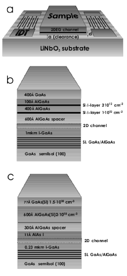
The heterostructure was considered as a multilayer system containing a thin conductive layer with complex sheet conductance at some distance from the bottom plane. Since the distance between the interface and the doped layer is much less than the SAW penetration depth the quantity is actually the effective conductance of the region including interface and doped layers, connected “in parallel”. Dielectric constants of two other layers (GaAs and Al0.3Ga0.7As, respectively) are assumed to be equal and denoted as . The heterostructure is placed on top of the LiNbO3 platelet with effective dielectric constant , the vacuum clearance between the heterostructure and the plate being denoted as . The clearance remains finite despite of the fact that the heterostructure was pressed to the piezoelectric platelet because of some roughness of both surfaces. Since the actual clearance is hardly controlled, the quantity is treated as an adjustable parameter. It is determined by fitting the experimental data at the steps between the Hall plateaus where the conductance is metallic and essentially frequency independent in the frequency region of our experiments. The values of are slightly different for different sample setups. For our experimental setup, cm.
According to the above model, components of the complex conductivity have been extracted from the experimental data from the expressions 4
| (1) | |||||
| (3) | |||||
Here is the electromechanical coupling constant for LiNbO3 (Y-cut), and are dimensionless functions allowing for electrical and geometrical properties of the sample, 4
II.2 Dependence of cooling rate
The acoustic measurements require the sample to be placed either in vacuum, or in a dilute gas. Otherwise SAW are strongly damped by the cooling liquid. In our experiment, the system consisting of the sample mounted on the LiNbO3 plate was placed on a cooling finger located in a chamber. The chamber was, in turn, placed in a He4 cryostat which can be pumped out to decrease its temperature. The superconductor solenoid in the cryostat was cooled by liquid nitrogen. To reach the temperatures K a dilute exchange gas (He4, 0.1 Torr) was inserted into the chamber, and that was the way to control the cooling rate.
The cooling procedure was as follows. The chamber containing the experimental setup has been initially cooled inside the cryostat by cold gaseous He4, and then liquid He has been poured into the cryostat.
Different cooling regimes were studied, and in the following they will be referred to as slow and rapid cooling. In the first case the exchange gas has been inserted from the very beginning, at the room temperature. Then the chamber was cooled during 1.5 - 2 hours by cold gaseous He4 down to 7 - 8 K, and finally liquid He was poured. In the second case, the chamber was initially evacuated and cooled first by gaseous and then by liquid He4, the sample temperature being monitored by a carbon thermometer. At some temperature , which actually depends on the pressure in the chamber, the exchange gas was inserted, and the sample cooled down to the cryostat temperature during 5-10 minutes. As a result, the cooling rate is an increasing function of , the maximum cooling rate being at K.
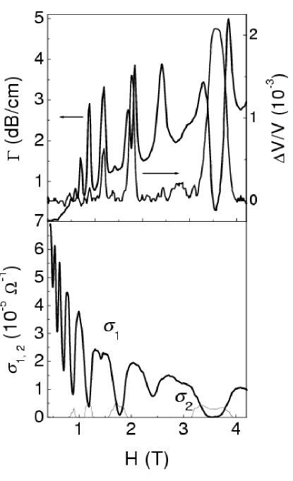
The results for a slowly-cooled of the Si -doped sample with the initial sheet electron density cm-2 are shown in the bottom panel of Fig. 2. They are extracted from the raw data shown in the top panel.
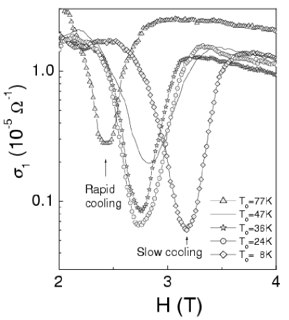
Magnetic field dependences for different cooling rates extracted at the same acoustic frequency, MHz, are shown in Fig. 3. One can observe that, depending on , (i) minimum values of are different, and (ii) minima occur at different values of magnetic field. Since all the minima correspond to the filling factor , it follows that the sheet electron density, , is a function of . The behavior of for and is similar.
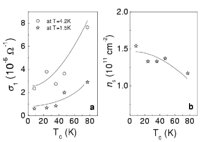
In Fig. 4, the values of and are plotted versus the pre-cooling temperature, . The first quantity increases with increase of , while the second one decreases. For all , imaginary part of the conductivity, , remains greater that that indicates hopping conductance. is also dependent on , however its dependence is much slower than that of . The general behavior of the ac conductance in the modulated-doped samples is similar.
The dependence of the sheet electron density turns out to be correlated with the initial value of ; the larger the initial the slower its dependence on . For the sample with cm-2 the relative variation of is 30%, for cm-2 is 10%, while cm-2 the dependence on is essentially absent. In the last sample the first band of size quantization is almost full.
It is worth noting that the state reached by fast cooling does not change for a long time. In particular, characteristics of the sample with cm-2 after maximally fast cooling from K did not change during at least 28 hours.
II.3 Dependence on illumination
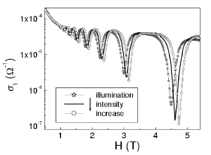
As well known, dc conductance of Al0.3Ga0.7As thin film 6 and GaAs/Al0.3Ga0.7As heterostructures Buks is sensitive to infrared (IR) illumination. To investigate combined effect of slow cooling and IR illumination on ac conductance light emitting diodes (LEDs) producing IR radiation with the wavelength and m were placed into the chamber Matveev . Choosing the illumination dose we were able to change the sheet electron density, as well as the ac conductance, by controllable portions. The persistent ac photoconductance is observed only if the illumination frequency exceeds some threshold located between 0.92 and 0.49 eV ( and m, respectively). The magnetic field dependence of after successive illumination of a -doped sample with cm-2 is shown in Fig. 5. One can see that successive pulsed illumination (pulse duration s) leads to a shift in the location of the corresponding minimum. The shift indicates an increase in the 2DEG density, . At the same time the minimum value of decreases.
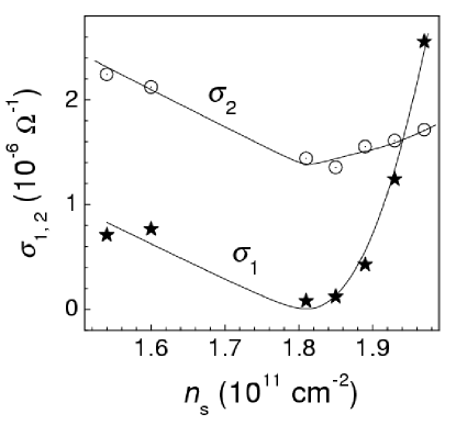
The effect of the illumination in a Si doped structure is illustrated in Fig. 6. Here and are plotted as functions of the sheet electron density , tuned by successive illumination. All three quantities are extracted from acoustic measurements at K. One can see that increase in is accompanied by decrease of down to to some value after which a rapid increase occurs. In this regime the successive illumination leads to an increase in leaving almost constant.
III Discussion
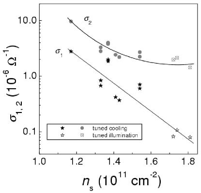
As we expected, 4 the set of experimental results indicates a significant role of the doped layer in the “memory” effects. Indeed, a remarkable feature of the experimental results is that, being presented as and versus , they are more-or-less universal. Namely, the data obtained for different cooling and illumination procedures collapse to almost same curves. To demonstrate this feature, in Fig. 7 we plot and versus for a Si -doped sample with initial electron concentration cm-2. Here the results both for different pre-cool temperatures and different illumination doses are included.
We believe that such property, as well as the threshold in ac photoconductance support the idea that the electron states in the doped layer are just the so-called centers. 6 These states are actually two-electron bound states stabilized by local lattice distortion. centers were observed both in GaAs/Al0.3Ga0.7As heterostructures and in AlxGa1-xAs films with . They are considered to be responsible for dc persistent photoconductance in these systems, which has also a threshold in the illumination quanta energy located between 0.66 and 0.8 eV 7 .
In general, the defects responsible for the -centers have three charge states which differ by number of electrons occupying the center. Due to a local lattice distortion the two-electron state has the lowest energy if the two electron correlation energy exceeds the thermal energy .comment As a result, at the the defects are either occupied by two electrons and negatively charged (-centers) or empty and positively charged (-centers) . The -centers can be treated as small bipolarons. The real situation is more complicated than the one discussed above since there is no unique opinion on the microscopic nature of excited states of the defect. In particular, there are several intermediate states of the defect each containing one electron, but differing by the amount of lattice distortion. In the following we will not discriminate between these states since detailed theory of acoustically-stimulated electron tunneling is beyond the scope of the present work. To simplify the discussion, following Ref. 8, , we assume that a set of equal number of and states form the ground state which is the only state occupied at very low temperature. The one-electron (neutral) state has the energy higher than the ground state energy by the correlation energy o.
In heterostructures, one can imagine several processes taking place during a cooling from the room temperature to 1.5 K. Among them are freeze-out of the carriers in the Si-doped layer of Al0.3Ga0.7As to occupy first deep states and then shallow states,9 carriers exchange between the doped and the interface layers, etc. We believe that under rapid cooling the electron distribution at the pre-cooling temperature is frozen - it does not significantly change during the cooling below . This statement is compatible with a crude estimate of the activation energy based on the expression eV which has been obtained for AlxGa1-xAs films for . 9 For our samples, this estimate yields meV. Consequently, varies from to as varies from 300 to 100 K.
Acoustic methods under conditions of the QHE provide a unique possibility to separate the contributions of the interface and doped layers. Indeed, at the QHE plateaus the electronic states in the interface layer are localized, and their contribution to are small. As a result, the contribution of the electron hopping in the doped layer becomes measurable. 4 We believe that the main mechanism leading to this contribution is due to tunneling transition of electron pairs (bipolarons) between a center and an adjacent one. At low temperatures sequential tunneling via the neutral states is probably not important since the energy difference between and the ground state is of the order of eV. However, states play an important role in the formation of the tunneling barrier between and centers. A theory of ac hopping conductance due to -centers in three-dimensional amorphous materials has been developed in Ref. 8, . According to this theory, is is rather difficult to discriminate between single-electron and two-electron tunneling from frequency and temperature dependences of . We are not aware of a theory of ac hopping conductance relevant to pair tunneling in GaAs/Al0.3Ga0.7As heterostructures. However, one can expect that the differences in frequency and temperature dependences are very small also in this case.
Assuming that the doped layer’s thickness is much less than we can use for an estimate similar to the well-known expression for the single-electron tunneling, 3
Here is the density of states for bipolarons, is their localization length, while is the electron charge. We believe that it is the density of states, , that is influenced by cooling and illumination procedures. In particular, the IR illumination causes ionization of the centers in the doped layer. Part of released electrons tunnels into the interface layer that results in the increase in the sheet density . A similar effect occurs during a rapid cooling due to quenching of the electron transfer between the defects and 2D layer. The higher the pre-cooling temperature the less time left for the electrons to tunnel into the interface layer. As a result, is a decreasing function of .
It worth mentioning that there is an important difference between the dc persistent photoconductance and the effect we observe. Indeed, in the first case the conductance is possibly due to extended electron states either in the 2DEG-layer or in the conduction band in Al0.3Ga0.7As layer. Contrary, the states responsible for the ac conductance are localized that follows from the relation . Illumination leads to a decrease in the number of occupied bound states. As a result, the ac conductance decreases with illumination. At very high illumination dose the centers become ionized, and all the ac conductance is due to extended states.
We have employed the procedure of Ref. 4, to separate the contributions of the doped layer and of the 2D layer in the ac hopping conductance and then analyzed the latter using a picture of single electron nearest-neighbor tunneling. Tuning the 2DEG density by illumination after slow cooling to change the magnetic field corresponding from 2.7 to 3.8 T we have found that the localization length in this region behaves as . This dependence is compatible with the assumption of the single electron nearest neighbor tunneling. Unfortunately, we were not able to carry out a similar analysis for since at large the components and are of the same order of magnitude, and the mechanism of ac conductance is mixed.
IV Conclusions
Main conclusions from the present work can be formulated as follows.
-
(i)
Both ac hopping conductance and sheet electron density in Si -doped and modulation doped GaAs/Al0.3Ga0.7As heterostructures at the quantum Hall effect plateaus depend on the samples’ cooling rate.
-
(ii)
Successive IR illumination leads to a persistent ac hopping photoconductance which decreases with the illumination dose. At the same time, the sheet electron concentration, , in the interface layer increases. The persistent ac photoconductance occurs only if the illumination frequency exceeds some threshold located between 0.5 and 0.9 eV.
-
(iii)
The above set of results can be qualitatively interpreted within the framework of the concept of centers – localized two-electron states bounded by local lattice distortion – located in the doped layer of the heterostructure. We believe that the doped layer ac hopping conductance is due to tunneling of electron pairs (bipolarons) between adjacent doubly occupied and empty defects.
-
(iv)
The contribution of tunneling between localized states in the interface layer can be extracted and used to estimate the electron localization length, . Within the experimentally-accessible range, which is compatible with single-electron nearest neighbor tunneling.
Acknowledgements.
One of the authors (ILD) is thankful B. A. Volkov and D. R. Khokhlov for discussions. The work is supported by RFFI 01-02-17891, MinNauki, Presidium RAN grants and Russia-Ukraine Program Nanophysics and Nanoelectronics.References
- (1) The Quantum Hall Effect, ed. by R. E. Prange and S. M. Girvin (Springer-Verlag, New York 1987).
- (2) A. Wixforth, J. Scriba, M. Wassermeier, J. P. Kotthaus, G. Weimann, and W. Schlapp, Phys. Rev. B40, 7874 (1989). R. L. Willett, R. R. Ruel, K. W. West, and L. N. Pfeiffer, Phys. Rev. Lett. 71, 3846 (1993). A. Schenstrom, Y. J. Quian, M. F. Xu, H. P. Baum, H. Levy, and B. K. Sarma, Sol. State Comm. 65, 739 (1988).
- (3) I. L. Drichko, A. M. D’yakonov, A. M. Kreshchuk, T. A. Polyanskaya, I. G. Savel’ev, I. Yu. Smirnov and A. V. Suslov, Fiz. Tekh. Poluprov. 31, 451 (1997) [Semiconductors 31, 384 (1997)].
- (4) I. L. Drichko, A. M. D’yakonov, V. D. Kagan, I. Yu. Smirnov, and A. I. Toropov, Proc. of 24th ICPS, Jerusalem, on CD-ROM (1998).
- (5) A. L. Efros, Zh. Eksp. Teor. Fiz. 89, 1834 (1985) [JETP 89, 1057 (1985)].
- (6) I. L. Drichko, A. M. Diakonov, I. Yu. Smirnov, Y. M. Galperin, and A. I. Toropov, Phys. Rev. B62, 7470 (2000).
- (7) D. V. Lang, R. A. Logan, Phys. Rev. Lett. 39, 635 (1977).
- (8) D. J. Chadi and K. J. Chang, Phys. Rev. B39, 10063 (1989).
- (9) P. M. Mooney, J. Appl. Phys. 67, R1 (1990).
- (10) E. Buks, M. Heiblum, and Hadas Shtrikman, Phys. Rev. B49, 14790.
- (11) N. V. Zotova, S. A. Karandashev, B. A. Matveev, A. V. Pentsov, S. V. Slobodchikov, N. N. Smirnova, N. M. Stus’, G. N. Talalakin, and I. I. Markov. Optoelectronic sensors based on narrow band A3B5 alloys, SPIE 1587 Chemical, Biochemical and Environmental Fiber Sensors III. pp. 334-345, Boston 1991.
- (12) A. E. Beljaev, Kh. Yu. von Bardeleben, E. I. Oborina, Yu. S. Riabchenko, A. I. Savchuk, M. L. Fije, M. K. Sheinkman, Fiz. Tekh. Poluprov. 28, 1544 (1994) [Semiconductors 28, 1544 (1994)].
- (13) Since the lattice distortion stimulates an attraction of two electrons at the center, the correlation energy is negative. Sometimes is called the Hubbard energy, and -centers are referred to as the centers with negative Hubbard energy.
- (14) M. Foygel, A. G. Petukhov, A. S.Andreyev, Phys. Rev. B48, 17018 (1993).
- (15) N. Chand, T. Henderson, J. Klem, W. T. Masselink, Russ Fisher, Yia-Chung Chang, H. Morkoc, Phys. Rev. B30, 4481 (1984).