Structure of Bi nanolines: using tight-binding to search parameter space
Abstract
We describe how we have used tight binding calculations as a quick, efficient tool to search for possible structures of Bi nanolines on Si(001). After identifying promising candidate structures, we have concentrated on these with ab initio electronic structure techniques. The energetics of the tight binding are shown to be in good agreement with the density functional calculations and with experimental observations, and have proved invaluable in the search for a structure, validating the use of tightbinding as a search tool.
I Introduction
When confronted with a new structure observed in experiment, or when trying to find possible pathways for reactions or diffusion events, there is often a need for performing electronic structure calculations on many different structures rather quickly, in order to search through parameter space efficiently. However, the need is not just for speed, but also for reasonable accuracy, as possible candidates must not be discarded out of hand. In this paper, we explore the use of tight binding as a tool to perform a search for the structure of Bi nanolines on Si(001), and consider future directions for these types of search using techniques developed over the last few years.
If a Bi-covered Si(001) surface is annealed at 570-600∘C, most of the Bi desorbs, but a small amount self-assembles to form nanolines, 1.5 nm wide and often over 400 nm longK.Miki et al. (1999a, b). These nanolines have great promise as templates for nanowiresJ.H.G.Owen et al. (2002a), when metals such as Al or Ga are deposited on them. However, to understand and control these processes and the growth of the nanolines, it is important to know their atomic structure; earlier proposals for the structureK.Miki et al. (1999a); D.R.Bowler (2000); M.Naitoh et al. (2000) have been shown to be wrong by recent experimental results, and a valid structure has only recently been found using a combination of STM and electronic structure modellingJ.H.G.Owen et al. (2002b). We describe the search for the structure, and the tools used for that search, in this paper.
Tight bindingC.M.Goringe et al. (1997) is a compromise between accuracy (it makes approximations, but preserves quantum mechanics) and computational efficiency (simulations of several hundred atoms can be run on a typical desktop workstation in a few hours). On semiconductor surfaces, where a rich variety of reconstructions exist, depending on a subtle interplay of electronic and geometric effects, the use of a quantum mechanical technique is vital if correct answers are to be found. We have developed parameterisations for Si(001), H on Si(001)D.R.Bowler et al. (1998a) and Bi on Si(001)D.R.Bowler (2000), and performed simulations on hydrogen diffusionJ.H.G.Owen et al. (1996); D.R.Bowler et al. (1998b, 2000a), gas-source growth of Si(001)J.H.G.Owen et al. (1997a, b, c); D.R.Bowler and M.G.Bowler (1998); D.R.Bowler and C.M.Goringe (1998) and Bi on Si(001)K.Miki et al. (1999a, b); D.R.Bowler (2000); J.H.G.Owen et al. (2002b) and have found that tight binding produces results which are in good agreement with both experiment and first principles techniques. In this paper, we further explore the use of tight binding as a tool to search through parameter space.
The problem we were faced with was that of finding the structure of the Bi nanolines. Various criteria had been found from experiment which possible candidates needed to fulfil: the lines must have a high kinking energy; the lines must occupy four Si dimers but lie between the substrate dimers; they must be more stable than the Bi-(2n) high coverage phase; and they must repel missing dimer defects and steps down. We needed an accurate, quantum mechanical technique that would allow us to test many possible structures quickly, allow us to have confidence in new reconstructions and distorted bonds, and that would also allow us to model large unit cells (to test kinking and defect repulsion) – a linear scaling or tight binding technique was found to be perfect. The rest of the paper describes the search: we start by describing the technical details of the modelling; we then consider the problem of modelling Bi on Si(001) and comparing structures with different amounts of Bi, and look at the stability of the Bi-(2n) high coverage phase; we present the details of various more or less successful models, and compare their energies to first principles calculations, and then we conclude.
II Technical Details
We performed tight binding simulations using a linear scaling technique (where the computational effort scales linearly with the number of atoms, not with its cube as is true for traditional techniquesS.Goedecker (1999)) as large cells, of up to several thousand atoms, were necessary to test the kinking and dimer repulsion properties of the nanoline structures. Specifically, we used an implementation of the Density Matrix Method (DMM)X.-P.Li et al. (1993) by GoringeC.M.Goringe (1995). We used tight binding parameterisations for Si-Si bonds developed specifically for Si(001)D.R.Bowler et al. (1998a) and for Bi on Si(001)D.R.Bowler (2000). The unit cells were always ten layers deep, with the bottom two layers constrained to lie in bulk-like positions, and terminated in hydrogen. For simple structure calculations, each cell was one dimer row wide (using the p() reconstruction) and sixteen dimers long (i.e. 384 atoms). When calculating kinking energies we used the same size cell, but four dimer rows wide (i.e. 1536 atoms). These methods have been used before with great success for calculations of many thousands of atoms (e.g. for calculation of step kinking energies on Si(001)D.R.Bowler and M.G.Bowler (1998)).
For an accurate assessment of promising candidates, we performed first principles density functional (DFT) simulations within the local density approximation (LDA) using the VASP codeG.Kresse and J.Furthmüller (1996). We used ultrasoft pseudopotentials, a plane wave cutoff of 150 eV (which gave energy difference and force convergence) and a Monkhorst-PackH.J.Monkhorst and J.D.Pack (1976) grid of k-points. Each unit cell was the same depth and width as the tight binding cells, but only eight dimers long, again with the bottom two layers held fixed in bulk-like positions and terminated in hydrogen. The change in energy caused by the shorter cell was found to be less than 0.1 eV; the longer tight binding cells were used to investigate nanoline-dimer repulsion, which could not be done using LDA.
A key question to consider when modelling the stability of structures with different chemical elements is how to compare structures with different stoichiometries. As the experiments we are considering were performed at high temperature on a Si(001) substrate, we can use the energy of bulk silicon to correct for different numbers of silicon atoms (though this raises questions about k-point sampling and error cancellation for the LDA calculations that will be considered below). For bismuth, however, we are faced with a harder problem. In the next section, we detail the approach used for calculating the periodicity of the high coverage Bi-(n) phase, and extract a sensible reference energy for Bi dimers on Si(001).
III Energetics of Bi on Si(001)
At high coverages, Bi forms rows of dimers on Si(001), relieving the strain due to the large difference in lattice constants by having missing dimer defects at regular intervals, forming a high coverage, Bi-(2n) reconstruction. As we see Bi nanolines forming within this (2n) surface (and we also see that the nanolines are more stable than it – they form while it is desorbing) we start by describing it. We approach this problem, which will involve different amounts of Bi, and hence different stoichiometries, in the same way that we have approached modelling of the Ge/Si(001) surfaceJ.Oviedo et al. (2002). It is perfectly easy to calculate the energy of formation of trenches of missing dimers simply by removing Bi dimers, but to make contact with experimental results we need to find an energy for these Bi dimers that we have removed. We shall assume that the Bi-covered surface is in thermal equilibrium (which is easy to arrange experimentally), so that for a given number of Bi atoms we can write the probability of any given arrangement of these atoms as proportional to , where is the energy of the arrangement. The assumption of thermal equilibrium greatly simplifies the system that we are considering, while being perfectly legitimate at a number of different temperatures.
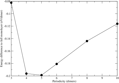
Now, as we are in thermal equilibrium, we only need know the relative energetics of different arrangements of the given number of Bi atoms. It will be useful to define a reference arrangement which we take to be a non-defective, lattice-matched layer of Bi covering a certain area of the Si(001) surface (with a boundary which we assume to be rectangular, but whose shape is arbitrary). Now we consider arrangements where we form regularly spaced trenches of missing dimers; conceptually we start by adding a number of dimers to the reference system equal to the number that we will remove and then forming the missing dimer trenches and relaxing. This conceptual approach allows us to compare different spacings by using the energy of Bi dimers in the perfect monolayer to correct for different amounts of Bi, which we find by calculating the difference in energy between a clean Si(001) surface and the same surface covered by a monolayer of Bi. Using our tight binding parameterisation we find this number to be -11.41 eV per Bi dimer.
We show the difference in energy per Bi dimer between a full, strained monolayer and the reconstructed surface for various values of period, n, in Fig. 1. There is a well defined minimum for periods of four and five (i.e. three and four Bi dimers) which is in excellent agreement with experimental observationsK.Miki et al. (1999a); Park et al. (1993). The modelling of this reconstruction gives us further confidence in our parameterisation, and presents a limit for the energetics of the Bi nanoline (which must be more stable than the Bi-(n) surface). Our tight binding simulations find that the energy per Bi dimer (adsorption energy and surface energy) in this reconstruction is -11.6 eV at n and n.
When considering structures with different amounts of Bi, we can use the fact that the nanolines are observed to form in the high coverage Bi-(2n) phase to extract a sensible reference energy for Bi dimers. We have chosen the energy to be -11.4 eV per dimer, the energy of the reference phase, and used this where necessary. As mentioned above, we use the bulk Si energy to correct for differing numbers of Si atoms.
IV Details of Successful Models
In this section, we present details of various of the models considered, and discuss how well tight binding has performed as a tool to discriminate between these models in the light of subsequent DFT modelling. First, we start by summarising the requirements placed on the models by experimental observations.
IV.1 Experimental Constraints
We have been able to distil a number of requirements for the nanoline structure from our experimentsK.Miki et al. (1999a, b); J.H.G.Owen et al. (2002a, b):
-
•
Stability: The lines form at a temperature where the high coverage (2n) Bi islands are evaporating, which implies that the energy per Bi dimer must be larger than these islands (in tight binding, more than -11.6 eV/dimer as given above). In RHEED experiments, the difference in desorption barrier for Bi from the islands and from the nanolines was determined to be 0.25 eVK.Miki et al. (1999a).
-
•
Width, Registration and Appearance: The nanolines run perpendicular to the Si(001) surface dimer rows, occupying the space of four Si dimers (15.36 Å). They consist of two dimer-like features separated by 6.3 Åwhich lie between the Si(001) dimers, but are in line with the dimer rows.
-
•
Straightness: Over many hundred observations of many lines (for instance in previous papersK.Miki et al. (1999a, b)), a kink has never been seen. Given the high temperature at which these nanolines form, it seems likely that a large thermodynamic kink energy is required, though a kinetic barrier cannot be ruled out.
-
•
Defect Exclusion Zone: The nanolines are observedJ.H.G.Owen et al. (2002b) to repel defects and down step edges to a distance of 3-4 nm. As the defects and steps have a tensile stress field, we expect that the nanoline model should also have a tensile stress field.
IV.2 Energetics from tight binding and DFT
Over the course of approximately a year, we have considered many different models. In general, we have first calculated the energy and kinking energy of possible models using tight binding. Only if these looked promising were they modelled with the more expensive DFT.
Within this section we present details of five unsuccessful models and what we believe to be the correct modelJ.H.G.Owen et al. (2002b), giving energies found with both tight binding and DFT. These results show that the tight binding calculations certainly ordered the structures correctly in terms of energy compared to DFT calculations (to within 0.1 eV) even though the absolute energies were sometimes rather too large, and thus confirm the use of this method as extremely valuable when searching a large configuration space. It is also worth noting that the tight binding simulations were computationally cheap (running in a matter of hours on a desktop workstation) and also that they deepened the collaboration between experiment and theory (many tight binding simulations were run by an experimentalist (JHGO), enabling detailed discussions of the remaining promising candidates). As an illustration, we found that tight binding relaxation calculations on a large unit cell used for kinking calculation (1536 atoms) took 2 hours and 4 minutes on a PowerMac G4/867MHz (using open-source g77 and ATLAS BLAS routines optimised for AltiVec) and 1 hour and 45 minutes on a Pentium 3/800MHz (using the Intel Fortran compiler for Linux and either ATLAS BLAS routines or the Intel Math Kernel library).
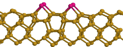
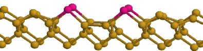
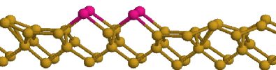
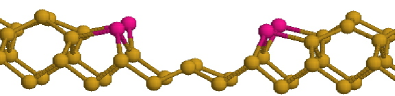
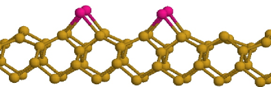
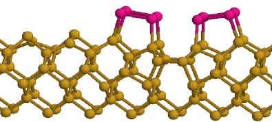
In Fig. 2 we show the ball-and-stick models of five unsuccessful candidates, and in Fig. 3 we show the final candidateJ.H.G.Owen et al. (2002b) (shown in off-axis views as the structures are rather complex). The five unsuccessful models shown are: the original structure proposedK.Miki et al. (1999a, b); D.R.Bowler (2000), which fitted original STM data but is only 3 Si dimers wide and has a very low kinking energy (labelled “Original”); the model proposed by Naitoh et al.M.Naitoh et al. (2000), which has the wrong spacing between features, is energetically poor and has a very low kinking energy (labelled “Two1DVs”); a structure made from back-to-back rebonded B-type steps, with Bi substituted in the second layer, which has the wrong appearance and is not energetically good enough (labelled “Btype4DV”); two Bi ad-dimers, which have no kinking energy and are energetically poor, and have no incentive to remain in this configuration (labelled “TwoAdDimers”); and two squares of Bi on top of a reconstruction similar to the final structureJ.H.G.Owen et al. (2002b) and to the structure of steps on As-covered Ge(001)S.B.Zhang et al. (2001).
| Model | TB (eV) | DFT (eV) |
|---|---|---|
| TwoSquares | 1.179 | 1.363 |
| TwoAdDimers | 1.565 | 0.848 |
| Two1DVs | 1.232 | 0.759 |
| Btype4DV | 0.611 | 0.564 |
| Btype3DV | 0.473 | 0.279 |
| Original | 0.000 | 0.000 |
| DoubleCore | -1.904 | -0.720 |
We give the energies for these models, along with a variation on the Btype4DV structure (the same structure but with only a 3 dimer width, which is energetically rather better, but has the wrong spacing and a low kinking energy, labelled “Btype3DV” and not illustrated) and the final candidate (labelled “DoubleCore”) in Table 1. Where the number of silicon atoms has differed from the clean surface, we have corrected using an appropriate value for the bulk energy for silicon. In the DFT calculations, it is questionable to use simply an energy calculated from a bulk Si cell, as the k-point sampling will differ unless fully converged in both cells; we also expect error cancellation to be better in the same sized unit cells. We approached the problem from two directions: first, we calculated the total energy of a clean Si(001) surface using both an eight layer and a ten layer slab, and used the energy difference to give us a value for the energy of bulk Si. We compared this to calculations of a bulk Si cell which were fully converged with respect to k-point sampling (we used a mesh, and checked with an mesh), and found that the energy difference less than 0.05 eV per atom. The energy that we used was 5.96 eV/atom.
From these energies, we can see that the tight binding calculations have correctly ordered almost all of the structures, though the energies are sometimes too large. It is extremely pleasing that it has performed so well for such a large variety of structures, especially the final candidate which contains a large stress and significant reconstruction. In particular, it can be seen that there are a wide range of bond lengths (Bi-Bi are generally about 2.9 Å, but Bi-Si vary from 2.60 to 2.82 Å) and angles (from to ) which the tight binding calculations have modelled correctly. Bi seems to favour bonding, with 90∘ bond angles and a pair of electrons in an s orbital – and the tight binding calculations have modelled this well. The only point where the ordering is wrong is for the TwoSquares structure, which tight binding found to be more stable than it should have been. The Bi-Bi bonds are generally shorter than found in DFT calculations (3.0-3.1 Å), suggesting that the Bi-Bi bond in TB might be too strong, accounting for the increased stability of this structure. The magnitudes of the TB energies are too large, probably because the model was fitted to bulk Bi-Bi and Bi-Si bonds, and this environment is at the surface, allowing Bi to form bonds with angles close to (its preferred bonding angle).
The unsuccessful models were rejected for a number of reasons: they were energetically poor (Two1DVs, TwoAdDimers, TwoSquares); they had the wrong appearance (Btype4DV and Btype3DV); they had a low kinking energy (Original, Two1DVs, TwoAdDimers, Btype3DV); they had the wrong spacing of Bi dimers (Two1DVs, Btype3DV, Btype4DV); they had the wrong registry of Bi dimers relative to the substrate (Original, Two1DVs); and they were less stable than the high coverage Bi-(2n) surface (Two1DVs, TwoAdDimers, Btype3DV, Btype4DV, TwoSquares).
The final candidate (DoubleCore) has the correct appearance, a high kinking energy (3.75 eV from tight binding calculations), the correct spacing of features (6.3 Å), a high repulsion for defects and down step edges (out to 6 or 8 dimers or 3 nm), and is more stable than the high coverage Bi-(n) surface. We have discussed this structure in more detail elsewhereJ.H.G.Owen et al. (2002b).
V Discussion and Conclusions
The key drawback with tight binding is that a parameterisation must be created for every interaction, and this is frequently a time-consuming procedure. Another extremely important problem for tight binding is that of transferrability: how well a parameterisation describes interactions that are dissimilar to the environment used for fitting. The Bi-Bi and Bi-Si parameterisation used was created simply and quicklyD.R.Bowler (2000), using the universal tight binding parameters of Harrison for Bi-Bi hoppingW.A.Harrison (1980) and fitting the scaling to the bulk modulus only; the parameterisations have only been used in environments close to those used for fitting. This simple procedure (which has also been applied to Ge-Ge and Ge-SiD.R.Bowler (2002)) has been shown here to be remarkably effective.
However, there is clearly a need for more reliable ways to explore parameter space in situations such as that encountered in this paper, and developments in the field known as ab initio tight binding are providing the answers. Starting with the Harris-Foulkes theoryJ.Harris (1985); W.Foulkes and R.Haydock (1989), the link between DFT methods using local, atomic-like orbitals and tight binding was shown. This was quantified in an elegant demonstration that tight binding could be derived from DFT via a well-defined series of approximationsA.P.Sutton et al. (1988). Ideas such as these have led to different approaches to improving and generalising tight binding.
Typically, confined atomic orbitals (found by solving the Schrödinger equation within a confining potential)O.F.Sankey and D.J.Niklewski (1989) are used as a basis set, adding orbitals beyond the minimal set as necessary for completeness. The problem with any approach like this is to decide where to make approximations. There are two key strands to these approximations: to neglect self consistency (but to retain three-centre integrals)O.F.Sankey and D.J.Niklewski (1989); and to add self-consistency but to neglect three-centre termsD.Porezag et al. (1995). Of course, there have been developments such as adding self-consistency to the three-centre approachA.A.Demkov et al. (1995).
The ultimate generalisation of these ideas lies in local orbital-based DFT methods such as SiestaD.Sánchez-Portal et al. (1997), PlatoA.P.Horsfield (1997); S.D.Kenny et al. (2000) and ConquestD.R.Bowler et al. (2000b), which point the way forward, as they enable the creation of the matrix elements (equivalent to a parameterisation) accurately, both in advance and in real time: the link between tight binding methods and DFT-based methods is becoming ever stronger. Clearly the level of approximation chosen needs to trade off against the size and complexity of the system being modelled.
In conclusion, we have presented tight binding and DFT calculations for the high coverage Bi-(n) surface which are in good agreement with experiment, and we have explored a variety of possible structures for Bi nanolines. Tight binding calculations have been shown to agree well with DFT calculations in terms of ordering structures, and enabled us to perform quick, efficient searches of parameter space. In particular, it has enabled us to find an extraordinary structure for the Bi nanoline, which in turn sheds light on the role of surface stress in self-assembly of nanostructures on semiconductor surfaces.
Acknowledgements.
DRB thanks the UK Engineering and Physical Sciences Research Council and the Royal Society for support through fellowships. JHGO is supported by the Japanese Science and Technology Agency (JST) as an STA Fellow. This study was performed through Special Coordination Funds of the Ministry of Education, Culture, Sports, Science and Technology of the Japanese Government (Research Project on active atom-wire interconnects). We are happy to acknowledge useful discussions with Dr. K.Miki, Prof. G.A.D.Briggs, Dr. W.McMahon and Prof. M.J.Gillan. DFT calculations were carried out in the HiPerSPACE Centre at UCL.References
- K.Miki et al. (1999a) K.Miki, J.H.G.Owen, D.R.Bowler, G.A.D.Briggs, and K.Sakamoto, Surf. Sci. 421, 397 (1999a).
- K.Miki et al. (1999b) K.Miki, D.R.Bowler, J.H.G.Owen, G.A.D.Briggs, and K.Sakamoto, Phys. Rev. B 59, 14868 (1999b).
- J.H.G.Owen et al. (2002a) J.H.G.Owen, D.R.Bowler, and K.Miki, Surf. Sci. Lett. 499, L124 (2002a).
- M.Naitoh et al. (2000) M.Naitoh, M. Takei, S. Nishigaki, N. Oishi, and F. Shoji, Jpn. J. Appl. Phys. Pt.1 39, 2793 (2000).
- D.R.Bowler (2000) D.R.Bowler, Phys. Rev. B 62, 7237 (2000).
- J.H.G.Owen et al. (2002b) J.H.G.Owen, K.Miki, and D.R.Bowler, Phys. Rev. Lett. submitted (2002b).
- C.M.Goringe et al. (1997) C.M.Goringe, D.R.Bowler, and E.H.Hernández, Rep. Prog. Phys. 60, 1447 (1997).
- D.R.Bowler et al. (1998a) D.R.Bowler, M.Fearn, C.M.Goringe, A.P.Horsfield, and D.G.Pettifor, J. Phys.: Condens. Matter 10, 3719 (1998a).
- J.H.G.Owen et al. (1996) J.H.G.Owen, D.R.Bowler, C.M.Goringe, K.Miki, and G.A.D.Briggs, Phys. Rev. B 54, 14153 (1996).
- D.R.Bowler et al. (1998b) D.R.Bowler, J.H.G.Owen, K.Miki, and G.A.D.Briggs, Phys. Rev. B 57, 8790 (1998b).
- D.R.Bowler et al. (2000a) D.R.Bowler, J.H.G.Owen, C.M.Goringe, K.Miki, and G.A.D.Briggs, J. Phys.: Condens. Matter 12, 7655 (2000a).
- J.H.G.Owen et al. (1997a) J.H.G.Owen, D.R.Bowler, C.M.Goringe, K.Miki, and G.A.D.Briggs, Surf. Sci. Lett. 382, L678 (1997a).
- J.H.G.Owen et al. (1997b) J.H.G.Owen, K.Miki, D.R.Bowler, C.M.Goringe, I.Goldfarb, and G.A.D.Briggs, Surf. Sci. 394, 79 (1997b).
- J.H.G.Owen et al. (1997c) J.H.G.Owen, K.Miki, D.R.Bowler, C.M.Goringe, I.Goldfarb, and G.A.D.Briggs, Surf. Sci. 394, 91 (1997c).
- D.R.Bowler and M.G.Bowler (1998) D.R.Bowler and M.G.Bowler, Phys. Rev. B 57, 15385 (1998).
- D.R.Bowler and C.M.Goringe (1998) D.R.Bowler and C.M.Goringe, Phys. Rev. B 58, 3937 (1998).
- S.Goedecker (1999) S.Goedecker, Rev. Mod. Phys. 71, 1085 (1999).
- X.-P.Li et al. (1993) X.-P.Li, R.W.Nunes, and D.Vanderbilt, Phys. Rev. B 47, 10891 (1993).
- C.M.Goringe (1995) C.M.Goringe, Ph.D. thesis, Oxford University (1995).
- G.Kresse and J.Furthmüller (1996) G.Kresse and J.Furthmüller, Comp. Mat. Sci. 6, 15 (1996).
- H.J.Monkhorst and J.D.Pack (1976) H.J.Monkhorst and J.D.Pack, Phys. Rev. B 13, 5188 (1976).
- J.Oviedo et al. (2002) J.Oviedo, D.R.Bowler, and M.J.Gillan, Phys. Rev. B submitted (2002).
- Park et al. (1993) C. Park, R. Bakhtizin, T. Hashizume, and T. Sakurai, Jpn. J. Appl. Phys. 32, L528 (1993).
- S.B.Zhang et al. (2001) S.B.Zhang, W.E.McMahon, J.M.Olson, and S.-H. Wei, Phys. Rev. Lett. 87, 166104 (2001).
- W.A.Harrison (1980) W.A.Harrison, Electronic Structure and the Properties of Solids (Freeman, San Francisco, 1980).
- D.R.Bowler (2002) D.R.Bowler, J. Phys.:Condens. Matter in press (2002).
- J.Harris (1985) J.Harris, Phys. Rev. B 31, 1770 (1985).
- W.Foulkes and R.Haydock (1989) W.Foulkes and R.Haydock, Phys. Rev. B 39, 12520 (1989).
- A.P.Sutton et al. (1988) A.P.Sutton, M.W.Finnis, Y.Ohta, and D.G.Pettifor, J. Phys. C 21, 35 (1988).
- O.F.Sankey and D.J.Niklewski (1989) O.F.Sankey and D.J.Niklewski, Phys. Rev. B 40, 3979 (1989).
- D.Porezag et al. (1995) D.Porezag, Th.Frauenheim, Th.Köhler, G.Seifert, and R.Kaschner, Phys. Rev. B 51, 12947 (1995).
- A.A.Demkov et al. (1995) A.A.Demkov, J.Ortega, O.F.Sankey, and M.P.Grumbach, Phys. Rev. B 52, 1618 (1995).
- D.Sánchez-Portal et al. (1997) D.Sánchez-Portal, P.Ordejón, E.Artacho, and J.M.Soler, Int. J. Quant. Chem. 65, 453 (1997).
- A.P.Horsfield (1997) A.P.Horsfield, Phys. Rev. B 56, 6594 (1997).
- S.D.Kenny et al. (2000) S.D.Kenny, A.P.Horsfield, and H.Fujitani, Phys. Rev. B 62, 4899 (2000).
- D.R.Bowler et al. (2000b) D.R.Bowler, I.J.Bush, and M.J.Gillan, Int. J. Quant. Chem. 77, 831 (2000b).