Stress relief as the driving force for self-assembled Bi nanolines
Abstract
Stress resulting from mismatch between a substrate and an adsorbed material has often been thought to be the driving force for the self-assembly of nanoscale structures. Bi nanolines self-assemble on Si(001), and are remarkable for their straightness and length – they are often more than 400 nm long, and a kink in a nanoline has never been observed. Through electronic structure calculations, we have found an energetically favourable structure for these nanolines that agrees with our scanning tunneling microscopy and photoemission experiments; the structure has an extremely unusual subsurface structure, comprising a double core of 7-membered rings of silicon. Our proposed structure explains all the observed features of the nanolines, and shows that surface stress resulting from the mismatch between the Bi and the Si substrate are responsible for their self-assembly. This has wider implications for the controlled growth of nanostructures on semiconductor surfaces.
Nanowires are of enormous importance for nanoelectronics: recently, various devices have been constructed from semiconductor nanowiresY.Huang et al. (2001) and carbon nanotubesA.Bachtold et al. (2001), to name but two. These approaches require assembly on the surface, whether by fluidics and patterning or use of scanning probes; self-assembled nanowires would be a compelling alternative for fabricating a large number of devices. However, the microscopic understanding of the underlying physical and chemical mechanisms for self-assembly of nanoscale features has been limited. Surface stress resulting from lattice mismatch in heteroepitaxial growth has often been thought to be responsible for self-assembly of nanoscale features (such as the growth of Ge ”hut” clustersD.J.Eaglesham and M.Cerullo (1990)). For the case of self-assembled nanowires on semiconductor surfaces, there has been much recent work on rare-earth silicides (e.g. ErSi2), where there is a large strain along one axis () and almost none along another, leading to the formation of extended nanowiresChen et al. (2000). These wires, however, are far from being uniform or perfect at the atomic scale. In contrast, Bi nanolines, formed when a Bi-covered Si(001) surface is annealed at around CK.Miki et al. (1999a, b), are quite striking in their uniformity. These nanolines are always 1.5 nm wide, and extend for hundreds of nanometres without a kink or a defect. As well as this, they repel defects and down B-type step edges to a distance of 3-4nm. Further, they are resistant to attack by radical hydrogen or oxygen (hence hydrogen can be used as a mask and oxygen used to isolate them electrically from the substrate)J.H.G.Owen et al. (2002), making them promising as templates for nanowires of other materials. However, the structure of these Bi nanolines, a prerequisite to a microscopic understanding of their unique properties and hence control of their nucleation and growth, remains unknown.
Earlier, we proposed a structure based upon a 3-dimer wide modelK.Miki et al. (1999a); D.R.Bowler (2000). However, recent atomic resolution scanning tunneling microscopy (STM) images of the Bi nanolineJ.H.G.Owen et al. (2002); M.Naitoh et al. (2000), have revealed that the structure in fact occupies the space of 4 dimers in the Si(001) surface. A proposed four dimer modelM.Naitoh et al. (2000) has the wrong spacing of features in the nanoline (ca. 5.4 Å), and is energetically very poor (more than 0.6 eV/Bi dimer worse than the 3-dimer modelD.R.Bowler (2000)). Moreover, neither model has a large kinking energy. Accordingly, we have conducted an exhaustive search for a new structure and tested many candidates against experimental criteria, which we detail below. For this purpose, semi-empirical tight binding (tb) calculations are invaluable, as they allow us to run large simulations of hundreds of atoms quickly on modest hardware(a desktop computer), while achieving relaxed energies very close to those obtained from ab initio density functional theory (DFT) calculationsD.R.Bowler (2000); D.R.Bowler and J.H.G.Owen (2002). In this paper, we propose a new structure for these nanolines that is energetically favourable and agrees with all experimental observations (size, stability, registry with Si dimers, straightness, repulsion of defects). We note that it is related to a structure recently proposed for B-type steps on As-terminated Ge(001) surfaces, and that our findings may well have implications for group V elements on group IV surfaces in general.
The Si(001) substrate was cleaned using a standard processK.Miki et al. (1998) before being transferred into vacuum. The Si surface was prepared by flashing repeatedly to 1100∘C for a few seconds, until there was only a small pressure rise. The clean surface was checked with STM before Bi deposition began. Bi was evaporated from an effusion cell, a typical dose being Bi at 470∘C for 10 mins. STM images were taken at the deposition temperature between 570-600∘C, and at room temperature, using a JEOL 4500 XT UHV STM. The high-resolution Bi 5d core-level photoemission spectra, taken at 65 eV photon energy, were measured on the new high-resolution vacuum ultraviolet beam line BL-1C at Photon Factory, KEK, Japan. The overall energy resolution was better than 100 meV. The relative stabilities of the proposed structures were calculated using two electronic structure techniques: for a swift search of possible motifs, tight binding; for accurate energies and structures, density functional theory(DFT). The tight binding calculations were performed with a linear scaling code (an implementation of the Density Matrix MethodX.-P.Li et al. (1993)) using a parameterisation which has been previously validated for Bi-Si interactionsD.R.Bowler (2000); this allowed the large unit cells necessary to model the long range strain effects seen in our STM data. The DFT calculations were performed using the VASP codeG.Kresse and J.Furthmüller (1996), using ultrasoft pseudopotentials, a plane wave cutoff of 150 eV (sufficient for energy difference convergence) and a Monkhurst-Pack k-point mesh with 441 points. The unit cell used had ten layers of Si, with sixteen atoms in each layer (forming a single dimer row with the p(22) reconstruction) with the bottom two layers constrained to remain fixed and dangling bonds terminated in hydrogen. When comparing energies with different amounts of Bi, we use unit cells of the same surface area, and compare the excess surface energy plus bismuth adsorption energy per Bi dimerD.R.Bowler (2000).
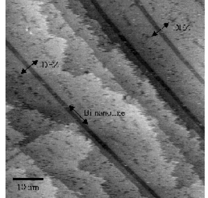
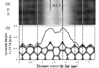
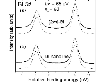
The Bi nanolines have several notable and unusual features. First, their straightness and perfection. Hundreds of lines have been observed, many over 400 nm long, without a kink being seen, and defects are extremely rare (their straightness can be seen in Fig. 1 and also in previous workK.Miki et al. (1999a, b)). This would suggest that the nanoline has a large kinking energy. Second, the “defect exclusion zone” (DEZ). Low concentrations of Bi embedded in the top layer of Si(001) cause compressive surface stress, and ordered trenches of missing dimer defects form every 8-12 dimers to relieve the stress. Despite being highly mobile at high temperatures, these defects do not come within 3-4 nm of the nanolines – the DEZ. Since the strain field of a missing dimer defect is tensile, the repulsive interaction between the defect and the nanolines suggests that the nanoline strain field should also be tensile, and hence is also a source of stress relief for the embedded Bi. It is likely therefore that the stress induced by the Bi in the top layer of the Si is the driving force for the formation of this unusual structure. Having formed, the nanolines remain after epitaxial islands of Bi have evaporated, indicating increased stability (RHEED experiments found the difference in desorption barrier to be 0.25eVK.Miki et al. (1999a)). However, the local structure of the Bi in the nanoline appears to be in a simple dimerized form, in the top surface layer. Recent high resolution STM images, such as in Fig.2 (a), and previous workM.Naitoh et al. (2000); J.H.G.Owen et al. (2002) show that the nanolines are 4 dimers or 15.4Åwide. The bright dimer-like features making up the nanoline lie between the underlying Si dimers, in line with the Si dimer rows. As marked, the spacing between the nanoline features is 6.3 Å. Photoemission spectroscopy experiments, shown in Fig.3, find that the Bi 5d core-level spectra of the Bi nanowire is essentially identical to the spectra of the (2n) phase composed of Bi ad-dimers, with a single well defined spin-orbit doublet. This suggests that the local chemical state and registry of Bi adsorbates for both phases are the same, i.e. that the Bi is in the form of dimers in the top layer of the structure. X-ray photo-electron diffraction (XPD) experimentsM.Shimomura et al. (2000) confirm the presence of Bi dimers parallel to the Si dimers and find the spacing between them to be 6.3Å. Hence, the observed properties of the Bi nanoline must result not from a novel Bi structure, such as a square of Bi atoms, but from an unusual Si substructure, stabilised by the presence of Bi.
A simple model for the line, with two Bi ad-dimers sitting on top of the dimer row, but between two Si dimers, as shown in Fig. 4(a), reproduces most of the aspects of the detailed STM data, and is consistent with the PES and XPD data, but is 0.53 eV/Bi dimer less stable than the (2n) phase, and has no energetic reason to grow long and straight; nor, indeed, is there any reason for the two ad-dimers to remain adjacent. However, our proposed structure may be reached from this simple structure by rearrangement of only a few atoms, illustrated in Fig. 4. A simple 2-dimer wide core (equivalent to half of our proposed structure) can be formed by rotation of the 2nd/3rd layer atoms, so that they lie on the same level. The resulting 2-dimer structure is quite similar to that proposed for the structure of As-Ge double-height B-type stepsS.B.Zhang et al. (2001). The energy of this structure is lower than the simple ad-dimer model, but the strain field of the core is compressive, the wrong sign for stress relief, and two such cores close together, necessary to form a 4-dimer unit, as shown in Fig. 4(b), repel each other. Removal of four central atoms and rebonding of 1st and 4th-layer Si atoms makes the overall strain field tensile, while keeping all bonds saturated (The terminating species is important; replacement of the two Bi ad-dimers by Si ad-dimers raises the total energy by 2eV/dimer). This gives our new proposed structure, shown in Fig. 4(c).
Our proposed structure is energetically very favourable and gives good agreement with all aspects of our experimental findings. In DFT calculations, the energy/Bi dimer is -10.9 eV/Bi dimer, 0.25 eV/Bi dimer lower than the high coverage Bi-(n) phase. This energy difference agrees very well with the difference in stability as measured by RHEED. Comparison of the structure to an STM profile yields extremely good agreement. A cross-section of the nanoline matched up with the ball-and-stick model is shown in Fig. 2(b). The position of the peaks of the Bi dimers line up perfectly with the STM profile. The spacing found from our calculations (6.25Å) and the direction of the Bi dimers (parallel to Si dimers) agree extremely well with photoemission spectroscopy and with XPD resultsM.Shimomura et al. (2000). Moreover, our proposed structure stands out from others that we have tested, in that it explains the other observed features of the Bi nanolines very naturally. The importance of surface strain relief in the formation of this structure is underlined by its increased stability in a surface terminated by Bi dimers. In this case, the total energy of a long tightbinding unit cell was further lowered by 0.1 eV/dimer, due to relaxation of the compressive stress in the surface Bi dimers. As expected, the tensile strain field of the nanoline also provides a driving force for the DEZ. Tightbinding calculations on a 32-dimer cell found that single missing dimer defects and step edges interact repulsively with the nanoline out to a range of 3 nm, in agreement with the observed DEZ width of 3-4 nm. The extensive distortion down to the fifth layer leads to a large kinking energy (3.75 eV/kink (tb)) and destabilises the dimers adjacent to the end of the line. The excess energy is 2.6 eV/line end in tightbinding calculations for an isolated line segment. We plan to report detailed calculations on all these features of the nanolines in future work.
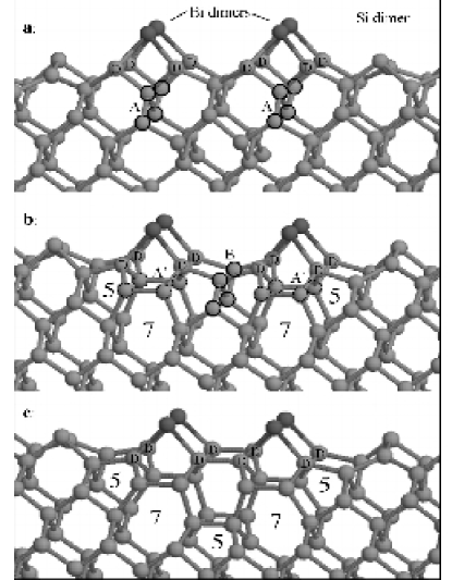
In conclusion, we have found an extraordinary structure for the Bi nanoline, which involves extensive reconstruction down to the fifth layer below the surface. Not only is this structure more stable than any other we have calculated, and matches extremely well with criteria drawn from a variety of experimental data, it also has an impressive ability to explain the notable and unusual properties of the Bi nanolines, such as the straightness (high kinking energy) and the defect repulsion (DEZ). The large tensile strain in one direction and zero strain in the other is very similar to the situation seen in the silicide nanowiresChen et al. (2000), and accounts for the invariant width and extreme length of the nanowire. Also of note are the 5-membered and 7-membered rings of Si, marked in Fig. 4 (b) and (c). Such odd-membered rings are also present in the proposed As-Ge step structure, suggesting that this structural motif may be of general interest in structures involving Group V layers on Group IV surfaces, particularly in situations where there is either compressive or tensile stress. Finally, the properties of these nanolines demonstrate the importance of surface stress in the formation and phenomenonology of nanoscale structures.
Acknowledgements.
The authors would like to thank Prof. Andrew Briggs(Oxford University) for useful discussions, and Bill McMahon for help with understanding the As-Ge structures. We are also happy to acknowledge Dr. Masaru Shimomura and Prof. Shozo Kono(Tohoku University) for detailed discussions about their XPD experiments. DRB acknowledges support from the EPSRC and from the Royal Society through fellowships, and the HiPerSPACE Centre (UCL) for computer time for DFT calculations. JHGO is supported by the Japanese Science and Technology Agency (JST) as an STA Fellow. This study was performed through Special Coordination Funds of the Ministry of Education, Culture, Sports, Science and Technology of the Japanese Government (Research Project on active atom-wire interconnects).References
- Y.Huang et al. (2001) Y.Huang, X.Duan, Y.Cui, L.J.Lauhon, K.-H.Kim, and C.M.Lieber, Science 294 (2001).
- A.Bachtold et al. (2001) A.Bachtold, P.Hadley, T.Nakanishi, and C.Dekker, Science 294 (2001).
- D.J.Eaglesham and M.Cerullo (1990) D.J.Eaglesham and M.Cerullo, Phys. Rev. Lett. 64 (1990).
- Chen et al. (2000) Y. Chen, D.A.A.Ohlberg, G. Medeiros-Ribeiro, Y.A.Chang, and R.S.Williams, Appl. Phys. Lett. 76, 4004 (2000).
- K.Miki et al. (1999a) K.Miki, J.H.G.Owen, D.R.Bowler, G.A.D.Briggs, and K.Sakamoto, Surf. Sci. 421, 397 (1999a).
- K.Miki et al. (1999b) K.Miki, D.R.Bowler, J.H.G.Owen, G.A.D.Briggs, and K.Sakamoto, Phys. Rev. B 59, 14868 (1999b).
- J.H.G.Owen et al. (2002) J.H.G.Owen, D.R.Bowler, and K.Miki, Surf. Sci. Lett. in press (2002).
- D.R.Bowler (2000) D.R.Bowler, Phys. Rev. B 62, 7237 (2000).
- M.Naitoh et al. (2000) M.Naitoh, M. Takei, S. Nishigaki, N. Oishi, and F. Shoji, Jpn. J. Appl. Phys. Pt.1 39, 2793 (2000).
- D.R.Bowler and J.H.G.Owen (2002) D.R.Bowler and J.H.G.Owen, Phys. Rev. B p. submitted (2002).
- K.Miki et al. (1998) K.Miki, K.Sakamoto, and T. Sakamoto, Surf. Sci. 406, 312 (1998).
- X.-P.Li et al. (1993) X.-P.Li, R.W.Nunes, and D.Vanderbilt, Phys. Rev. B 47, 10891 (1993).
- G.Kresse and J.Furthmüller (1996) G.Kresse and J.Furthmüller, Comp. Mat. Sci. 6, 15 (1996).
- M.Shimomura et al. (2000) M.Shimomura, K.Miki, T.Abukawa, and S. Kono, Surf. Sci. Lett 47, L169 (2000).
- S.B.Zhang et al. (2001) S.B.Zhang, W.E.McMahon, J.M.Olson, and S.-H. Wei, Phys. Rev. Lett. 87, 166104 (2001).