Spin-dependent Transparency of Ferromagnet/Superconductor Interfaces
Abstract
Because the physical interpretation of the spin-polarization of a ferromagnet determined by point-contact Andreev reflection (PCAR) is non-trivial, we have carried out parameter-free calculations of PCAR spectra based upon a scattering-theory formulation of Andreev reflection generalized to spin-polarized systems and a tight-binding linear muffin tin orbital method for calculating the corresponding scattering matrices. PCAR is found to measure the spin-dependent interface transparency rather than the bulk polarization of the ferromagnet which is strongly overestimated by free electron model fitting.
pacs:
72.25.Ba, 74.80.Fp, 71.15.Ap]
The spin-polarization of a ferromagnet at the Fermi energy (not to be confused with the total magnetic moment) is a parameter of crucial importance entering all models of magneto-electronic phenomena such as tunneling magnetoresistance (TMR). Although Moodera et al.’s TMR experiments [1] could be interpreted in terms of bulk spin-polarizations using a very simple model due to Julliere [2], subsequent experiments on a wider variety of materials cast doubt on the general validity of the model [3, 4, 5]. They also led to the need to find simpler ways of measuring spin-polarizations than the benchmark determinations by Tedrow and Mersevey [6] using tunneling spectroscopy at ferromagnetinsulatorsuperconductor (SIF) junctions. These are difficult to make and characterize, especially for complex materials. Andreev reflection spectroscopy at ferromagnet-superconductor (FS) interfaces in ballistic point contacts (PCAR) has been proposed as a simpler and complementary method to measure spin polarizations [7, 8, 9]. When the diameter of the point contact is smaller than the mean free path but larger than the Fermi wavelength, transport is governed by the Sharvin resistance [10], appropriately modified to take into account the interface “transparency”. In the Blonder-Tinkham-Klapwijk (BTK) theory [11], this is done by representing the interface as a planar -function barrier between free-electron materials. The Bogoliubov-de Gennes equation [12] for a normal-superconducting (NS) interface is readily solved for this model and the essential physics expressed in terms of a dimensionless barrier strength and the superconducting energy gap . At the interface to a ferromagnetic material, the Andreev reflection is suppressed by the difference between majority and minority electronic band structures [13]. Using the parabolic-band Stoner-Wohlfarth model for ferromagnetic materials, BTK theory can easily be generalized to spin-polarized systems. With only a single additional parameter , the spin polarization of the ferromagnet, a good fit to experimental data is apparently achieved [7, 9].
In spite of this, doubts have been raised about the definition and physical significance of the parameter derived from different experiments for all but 100% polarized ferromagnets [14]. Apart from concerns about the relevant Fermi surface averaged quantity to be used to describe different transport regimes, transport through an interface should not depend solely on parameters characteristic of bulk materials. The representation of an interface between materials with quite different electronic structures as a -function barrier can only be justified in terms of analytical simplicity. The free-electron Stoner model does not describe itinerant ferromagnetism in transition metals in an internally consistent manner and the probability of Andreev reflection is overestimated by such models; complex transition metal Fermi surfaces lead to a reduction of the phase space available to an electron to pair with a spin-flipped retro-reflected hole.
In this letter we present a generalized scattering formalism of Andreev reflection [15, 16] to spin-polarized systems and calculate the PCAR spectra with and without interface disorder. By basing our study on ab-initio calculations we can treat the full complexity of the transition metal band structure without introducing any arbitrary parameters and make contact with experiments for a number of systems of current experimental interest. We will be forced to conclude that the generalized BTK model omits an important aspect of the problem, basically because the bimodal distribution of the transmission probabilities of real interfaces are inaccurately modelled using a -function potential.
We start with the Bogoliubov-de Gennes [12] equation for the electron and hole wave functions of a superconductor
| (1) |
where . is the single-electron Hamiltonian matrix for majority and minority spins. are the coefficient-vectors of the wave functions of electrons (holes) in some convenient basis. The excitation energy is measured relative to the Fermi energy. Following Beenakker [15], wave-function matching at the FS interface is achieved by inserting between F and S a fictitious region in which S assumes its normal state (disregarding the proximity effect). At the FN interface, the scattering of the Bloch states for electrons and holes can be written
| (2) |
where denotes right(left) going waves and
| (3) |
is the normal-state scattering matrix. The subscript 1 refers to F, 2 to N. At the (fictitious) NS interface there is only Andreev scattering:
| (4) | |||||
| (5) |
where for , describes the phase shift due to the penetration of the wave function into the superconductor and for , , . The incoming and reflected waves are related on the F side by
| (6) |
| (7) | |||||
| (8) |
| (9) |
are the reflection coefficients for the total system. In terms of the spectral conductance
| (10) |
and the Fermi-Dirac distribution function , the current-voltage relation is . The charge transport in the presence of Andreev reflection is thus expressed in terms of the scattering matrix for the normal state. This expression is the spin polarized generalization of Beenakker’s formula [15] and reduces to the BTK equivalent if we use the scattering matrix of a -function potential and the parabolic band model. Note that the expressions also hold for energies above the superconducting gap.
The parameter-free calculation of the reflection matrices [17] and the conductance (10) is based on the surface Green’s function method [18] implemented with a tight-binding linear muffin tin orbital basis[19]. Because a minimal basis set is used, we are able to carry out calculations for large lateral supercells and model disorder very flexibly within such supercells without using any adjustable parameters. The electronic structure is determined self-consistently within the local spin density approximation. For disordered layers the potentials are calculated using the layer CPA approximation [18].
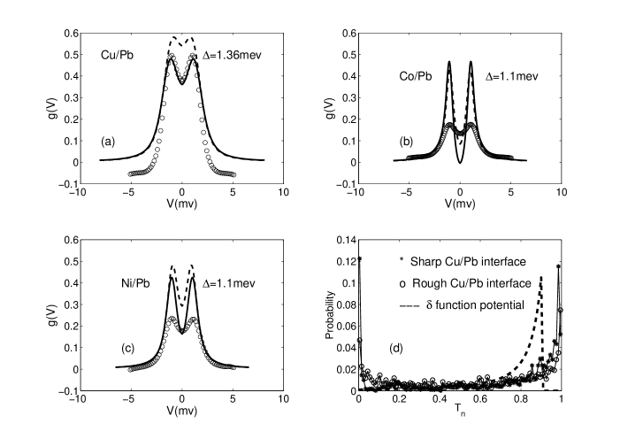
We focus our attention here on the Cu/Pb, Co/Pb and Ni/Pb systems investigated experimentally in [7] which were grown with an fcc(111) orientation in point contacts. We encounter the practical difficulty that the lattice constants of Pb are quite different from those of Cu, Co and Ni. Lattice matching is modelled using lateral supercells containing Cu (Co or Ni) atoms on one side of the interface and Pb atoms/monolayer on the other side or Cu, Co or Ni and Pb atoms/monolayer which gives better matching but is computationally more expensive. Disorder is taken into account by introducing a two monolayer-thick 50% interface alloy [17]. The results are not very sensitive to moderate variations in the alloy concentration in this range. Experiments [7] have been carried out at slightly elevated temperatures to suppress a possible proximity effect. Our computations are therefore carried out using the corresponding values of kT in the Fermi function: 4.2 K for Cu/Pb, 1.4 K for Co/Pb and 2.5 K for Ni/Pb. The only parameter in the calculations is the superconducting energy gap which is taken from experiment and is very close to the bulk value.
For an ideal NS interface Andreev reflection leads to a doubling of the conductance. In Table I the zero bias values , calculated for clean and alloy interfaces, are compared with the experimental values of Ref.[7]. Suppression of the Andreev reflection is apparent in all three cases but is smallest for non-ferromagnetic Cu. Even there, however, bandstructure mismatch between Cu and Pb gives rise to a significant reduction of the interface transparency and suppression of AR. The agreement with experiment is remarkably good and only in the case of Co/Pb is there any indication of a discrepancy. This picture changes when we compare the calculated and experimental spectra in Fig. 1 shown in terms of where is the normal state conductance and is the differential conductance for an FS interface at finite temperature and finite bias.
Let us first focus on the paramagnetic Cu/Pb point contact, Fig. 1(a). Whereas results for a specular interface deviate significantly from the measured data, the decreased conductance of a rough interface leads to essentially perfect agreement with experiment. Aspects of the problem not taken into account, like spin-orbit scattering and strong-coupling superconductivity in Pb are apparently not very important.
The agreement with the PCAR spectra for the ferromagnetic systems (Figs. 1(b) and (c)) is not satisfactory close to the band edge of quasi-particle excitations, where the theoretical results appear to strongly exaggerate the Andreev reflection [20]. Since we have no parameters with which we could improve the agreement the deviations should be sought in deficiencies of the model. For example, the close proximity of the ferromagnet might smear out the peaked density of states of the superconductor at the band edges [21]. Whereas this point deserves attention, we focus in the following on the zero-bias conductance.
The spin-polarization of the interface conductance, , will in general differ from that of the bulk ferromagnetic material. For example, for Ni/Pb, for a specular interface and for a rough interface. This should be compared to the BTK fit obtained in Ref. [7] of . Our prediction of a small spin-dependence of the interface conductance could be tested directly by measuring the magnetoresistance of a Ni/Pb/Ni trilayer (or multilayer) in the current-perpendicular-to-the-plane configuration with the layer thickness chosen sufficiently thin that the total resistance is dominated by the interface contribution. Using the expression given by Schep et al.[22] for diffuse systems, we predict interface resistances of and for a rough Ni/Pb (111) interface.
We emphasize the difference between the single-channel BTK model and the multichannel scattering theory generalization by focusing on the zero-voltage, zero-temperature conductance (10) for a non-magnetic system:
| (11) |
is expressed in terms of the eigenvalues of the transmission matrix, , and the sum is over the propagating channels [15]. For the Cu/Pb interface, the distribution function of transmission matrix eigenvalues, , is shown in Fig. 1(d). It turns out to be a bi-modal function with a clear dependence on interface roughness and on the constituent materials. Obviously, strongly affects the Andreev reflection probability with the main contribution coming from the highly transmitting part, whereas the average conductance is much more affected by the low transmission channels. Using the Andreev conductance to derive an average transmission is therefore misleading. For a -function potential and free electrons the transmission probability as a function of the in-plane wave vector has the form . The distribution function for , the value which must be taken to reproduce the average conductance, is plotted as a dashed curve in Fig. 1(d) and is seen to be qualitatively incorrect compared to the realistic distributions.
For the FS interface the situation is more complicated. Since Cooper pairs are phase sensitive, the conductance is governed by the full scattering matrix, ı.e. by the scattering amplitudes and not just the transmission probabilities. We therefore cannot use a single distribution function to characterize the interface because the Andreev reflection probability contains terms like which cannot be expressed by and . Still, it should be clear that the deficiencies of the function barrier potential will not vanish.
In summary we calculate the PCAR spectra of Co/Pb, Ni/Pb, and Cu/Pb point contacts and the spin-polarization of Co/Pb, Ni/Pb interfaces from first principles which allows us to remove what is a dubious approximation made when applying the BTK model to transition metals. We find good agreement with experimental results by the Cornell group for the full spectrum of Cu/Pb and for the zero bias conductance in the ferromagnetic systems. Qualitative differences are revealed by comparing our results with that of a simple BTK model. The physical significance of parameters obtained by fitting experiments with this simple model is doubtful.
This work is supported by the Stichting FOM, the NEDO International Joint Research Grant Program “Nano-magnetoelectronics”, the Grant Agency of the Czech Republic (202/00/0122), the European Commission’s TMR Research Network on “Interface Magnetism” (contract No. FMRX-CT96-0089) and RT Network “Computational Magnetoelectronics” (contract No. HPRN-CT-2000-00143). We acknowledge fruitful discussions with W. Belzig, A. Brataas, Yu. Nazarov, and J. Kudrnovsky and thank R.A. Buhrman for providing us with the experimental data shown in Figure 1.
REFERENCES
- [1] J. S. Moodera et al., Phys. Rev. Lett. 74, 3273 (1995); Phys. Rev. Lett. 80, 2941 (1998).
- [2] M. Julliere, Phys. Lett. 54A, 225 (1975).
- [3] M. Sharma, S. X. Wang, and J. H. Nickel, Phys. Rev. Lett. 82, 616 (1999).
- [4] J. M. De Teresa et al., Phys. Rev. Lett. 82, 4288 (1999); Science, 286, 507 (1999).
- [5] P. LeClair et al., Phys. Rev. Lett. 84, 2933 (2000); Phys. Rev. Lett. 86, 1066 (2001).
- [6] R. Meservey and P. M. Tedrow, Phys. Rep. 238, 173 (1994) and references therein.
- [7] S. K. Upadhyay et al. Phys. Rev. Lett. 81, 3247 (1998); Appl. Phys. Lett. 74, 3881 (1999).
- [8] R. J. Soulen et al., Science 282, 85 (1998); B. Nadgorny et al. Phys. Rev. B 61, R3788 (2000).
- [9] Y. Ji et al., Phys. Rev. Lett. 86, 5585 (2001).
- [10] Y.V. Sharvin, Zh. Eksp. Teor. Fiz. 48, 984 (1965) [Sov. Phys. JETP 21, 655 (1965)].
- [11] G. E. Blonder, M. Tinkham, and T. M. Klapwijk, Phys. Rev. B 25, 4515(1982).
- [12] P.G. de Gennes, Superconductivity of Metals and Alloys, (Addison Wesley, 1966)
- [13] M.J.M. de Jong and C.W.J.Beenakker, Phys. Rev. Lett. 74, 1657 (1995).
- [14] I. I. Mazin, Phys. Rev. Lett. 83, 1427 (1999).
- [15] C.W.J. Beenakker, Rev. Mod. Phys. 69, 731 (1997).
- [16] G.B. Lesovik, A.L. Fauchere, and G. Blatter, Phys. Rev. B 55, 3146(1997).
- [17] K. Xia et al., Phys. Rev. B 63, 064407 (2001).
- [18] I. Turek et al., Electronic Structure of Disordered Alloys, Surfaces and Interfaces (Kluwer, Boston-London-Dordrecht, 1997).
- [19] O.K. Andersen, O. Jepsen, and D. Glötzel, in Highlights in Condensed Matter Theory, edited by F. Bassani, F. Fumi and M. P. Tosi (North-Holland, Amsterdam, 1985), p. 59.
- [20] Similar results for clean Cu/Pb and Co/Pb interfaces have been reported by F. Taddei, S. Sanvito, and C.J. Lambert in J. of Low Temp. Phys. 124, 305 (2001) using a multiband tight-binding model. In our self-consistent calculations for Co/Pb we find no evidence for an enhancement of the exchange splitting at the interface which these authors invoke to obtain agreement with experiment for Co/Pb.
- [21] K. Halterman and O.T. Valls, Phys. Rev. B 65, 014509 (2002).
- [22] K.M. Schep et al., Phys. Rev. B 56, 10805 (1997).
| Cu/Pb | Ni/Pb | Co/Pb | |
|---|---|---|---|
| Clean Interface | 1.54 | 1.29 | 1.08 |
| Alloy Interface | 1.36 | 1.16 | 1.00 |
| Experiment | 1.38 | 1.18 | 1.13 |