Magnetic and Transport Properties of Trilayers
Abstract
Magnetic coupling between double thin films separated by an insulating spacer layer is investigated with structural measurements, cross sectional imaging, magnetization measurements (BH loop) and transport under the conditions of variable spacer thickness ranging from 0 to 5000 Angstroms. We investigate several models to explain the coercivity variation with spacer thickness as well as the transport measurements.
pacs:
75.00.00, 73.43.Qt, 74.25.Ha, 85.70.-w, 85.70.KhI. INTRODUCTION
Mass Storage, Sensing, Spintronics, Quantum computing and other applications
of magnetic thin-film devices are driving the current interest in
understanding the nature and extent of magnetic exchange interactions and
coupling effects arising between layers and nanostructures. While most
investigations have focused on metal-sandwiched multilayer systems like
Fe/Cr and Co/Cu where the thickness of the metallic material between the
ferromagnetic layers determines whether the interlayer coupling will be
ferromagnetic or antiferromagnetic, this work is focused on ferromagnetic
layers sandwiching an insulating or semiconducting spacer of variable
thickness. These systems are of interest in the study of e.g. read heads
made from multilayered films laminated with insulators (usually
) to prevent eddy currents or magnetic tunnel junctions using
two magnetic layers with different coercivities, separated by a thin
insulating layer (1 to 2 nm thick). One of the most striking effects of this
coupling, is the reduction of coercivity of a single layer, attributed to
reduced domain wall energy, that may alter drastically the device behavior.
Several possibilities exist and have been studied to describe interactions
between two ferromagnetic layers across an insulating or semiconducting
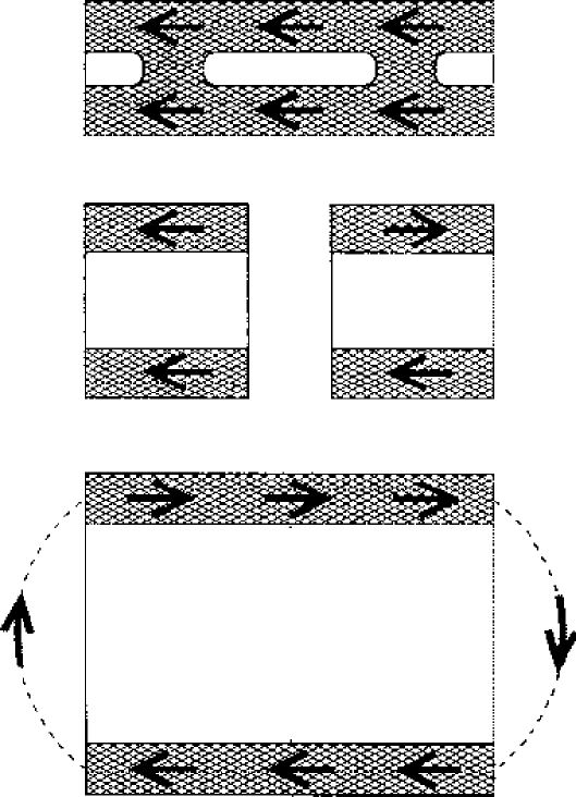
layer platt (see Fig. 1). Pinholes generally mediate direct ferromagnetic
coupling between neighbouring multilayers. They are viewed like shorts
across the insulating or semiconducting layer. Néel proposed that conformal
roughness (orange-peel model) at interfaces can result in ferromagnetic
coupling for a moderate thickness of spacer material. Recently, an
uncorrelated roughness model for biquadratic coupling has been proposed as
well strijkers . In Néel model, roughness features on the surface of the bottom
ferromagnetic layer propagate through the uppermost layers as they are
deposited platt .
Magnetostatic coupling occurs between the roughness features or between
domain walls in the two magnetic layers. In this case, stray flux fields
from walls in one film can influence the magnetization reversal process in
the other.
Slonczewski loose-spin model strijkers is based on the change in angular momentum experienced by spin-polarized electrons tunneling across a spacer barrier resulting in a magnetic exchange coupling. The magnitude and sign of the coupling oscillates depending on the interfacial barrier properties.
This work aim is to collect various structural, layer morphology, magnetic (mainly BH loop and coercive field measurements) and transport evidences in order to discriminate among all these different models.
II. SAMPLE PREPARATION
The trilayer samples in this study were grown by RF sputtering onto Corning 7059 Glass substrates at nominal room temperature. The wafers were mounted on a rotating substrate table that passes the wafers over individual sputtering guns. The sputtering gas used is mbar of Ar in a background pressure of mbar and an RF power density of 1W/cm2. The base magnetic layer is 480 Å of Permalloy ( alloy denoted as Py) with as the spacer material, and another top layer of Py 480 Å thick. Each magnetic film was sputtered from a composite target. The was also RF sputtered from an oxide target at a power density of 1W/cm2. The thickness of the Py layers was monitored precisely and kept constant. Its value was carefully chosen in order to minimise Hc for this type of structure (In Fig.2 the morphology of the trilayer is shown with a special High Resolution TEM technique). The magnetization of all the Py films was planar in all the samples studied.
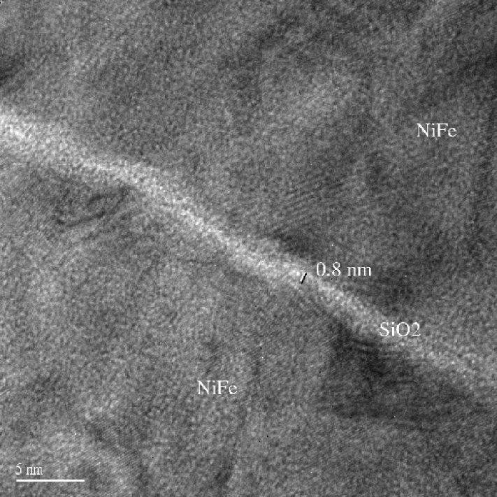
Clearly, a small undulation is visible in the TEM image (with an average amplitude h 1 nm and wavelengh 30 nm) indicating that the roughness of the layer at the two interfaces with the Py layers is conformal and might play a role in the physical properties as discussed later.

The amorphous nature of the structure is demonstrated by the X-Ray diagram shown in Fig.3. The sharp feature appearing in the diagram corresponds to the presence of microcrystallites of Py type with a textured growth along (111) direction.
III. HYSTERESIS LOOP MEASUREMENT
The trilayers showed marked anisotropic magnetization behavior in hysteresis
BH loop measurements. On the average, the anisotropy field observed in the
the hard axis configuration of the BH loop was about 4 Oe. That is not the
case of the easy axis coercivity as described in the next section. We
believe that our samples possess a uniaxial anisotropy character as shown by
Platt et al. platt whose high-field torque measurements confirm the presence
of a uniaxial anisotropy, under similar conditions.
Several sets of BH loop measurements were performed in addition to understand and assess the true nature of the coupling between the layers. We performed measurements on raw films, uncoupled layers, saturated layers and finally fully coupled layers.
IV. COERCIVITY MEASUREMENTS
Magnetic coupling between double thin films separated by the insulating
spacer layer is investigated with magnetization measurements (BH
loop) under the conditions of variable spacer thickness ranging
from 0 to 5000 Å.
The easy axis coercive field Hc displayed in Fig. 4 decreases, then shows a fine structure in the form of damped oscillations to increase again with the thickness of the spacer layer. The drop of the coercivity Hc compared to the free Py layer may attain a factor of 15 under certain conditions. For larger values of thickness, the magnetization reversal becomes sharper. In addition, when the spacer layer is thicker than 100 Å, separate reversal of the magnetic layers is observed in the hysteresis loop.

V. TRANSPORT MEASUREMENTS
Magnetoresistive devices have transport properties that depend on the
relative orientation of magnetic moments in neighboring grains or thin
films. Application of an external magnetic field along different axes (easy
and hard axes of Py) and with respect to the injected current direction
J results in a specific dependence of scattering on spacer
thickness. The key to understanding of the scattering is based on domain
wall orientation in the layers viret .
The in-layer magnetic domain wall structure is the source of scattering for the injected electrical current in the structure. Fig. 5 displays, respectively, the easy axis (EA) coercive field Hc with a damped oscillating fine structure (for an thickness 0.6 to 3 nm) and the corresponding magnetoresistance ratio MR values defined as where et are measured with and without the saturation magnetic field. Magneto-transport data were taken with a high resolution four-point probe with the current J flowing either parallel to the domain wall, i.e. parallel to the easy axis (EA) or perpendicular to the domain wall, i.e. parallel to the hard axis (HA). The magnetic field B is applied either parallel to the current J direction (B J) or perpendicular to J (B J). The coupling between the layers alters the domain wall configuration and thus modulates the scattering affecting the magnetoresistance. Different orientation of the domain walls for different thickness has been studied extensively in the past feldtkeller and the transport data correlate well with Hc fine structure as discussed next.

VI. DISCUSSION AND CONCLUSIONS
Our study reveals that the EA coercivity field is a powerful probe to test
magnetization reversal processes in magnetically ordered and artificially
structured magnetic materials. For any given material Hc depends on
coupling reflecting the average properties of the sample as well as local
interactions such as wall-wall interaction or magnetization anisotropy
dispersion (ripples), in addition to some intrinsic quantities (such as the
effective anisotropy and saturation magnetization). This paves the way to
manufacture ultra-soft artificial magnetic nanostructures, e.g. our
structure was so soft (in comparison with a single layer of same thickness)
that the fine structure in Hc may be viewed as some kind of magnetic
imaging of wall topography in coupled thin films.
The observed decrease in Hc is more pronounced for the EA field direction, where the magnetization process is determined by domain wall motion. The internal flux closure of the Néel-wall like structures leads to a reduced interaction in the film and between walls in coupled layers, resulting in a drop of Hc. In addition, we believe that wall character changes are driven by coupling in the following way. If the magnetization is reversed by wall motion, the effect of the coupling will be that both Py film magnetizations are reversed simultaneously. This means that a wall in one film is always close to another in the other film. Because of the dipolar magnetic moment of the Néel-walls there will be a magnetostatic interaction between the walls (in addition to an eventual coupling in the case of loose spins at the interface or pinhole presence). Following feldtkeller , the resulting configurations are shown in Fig. 6.
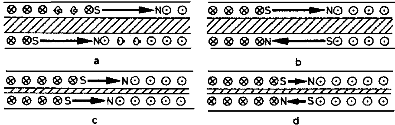
Two principally different configurations must be considered, one with the
magnetization of both walls parallel (Fig. 6a and c), and another with
anti-parallel magnetizations. When the coupling is weak, the arrangement
will be governed by magnetostatic interaction yielding the configuration
shown in Fig. 6a and b. For a stronger coupling (due to a thinner
intermediate layer (or with loose spins at interfaces or pinholes), the
configurations shown in Fig. 6c and d must be expected. The configuration of
Fig. 6c and d will have a wall energy larger than those of Fig. 6a and b. In
addition, specific energy conditions in the film (generally of magnetostatic
origin), favor a local ferro or antiferromagnetic-like coupling (see Fig.
5). We estimate following bobo and by looking at Fig.2 that
orange-peel coupling, induced by the roughness of the layers is
negligible in our case.
In conclusion, our work illustrates the detailed study of the nature of the
coupling between two magnetic layers separated by an insulator spacer of
variable thickness.
Acknowledgements: The authors thank J. Ostorero, F. Michaud and X. Castel for the X-Ray measurements and E. Snoeck for the cross section TEM microscopy.
References
- (1) C.L. Platt, M.R. Mc Cartney, F.T. Parker and A.E. Berkowitz, Phys. Rev. B 61, 9633 (2000), F.J. Himpsel, J.E. Ortega, G.J. Mankey and R.F. Willis, Adv. in Phys. 47, 511 (1998).
- (2) G.J. Strijkers, J.T. Kohlhepp, H.J.M. Swagten and W.J.M. de Jonge, Phys. Rev. Lett. 84, 8 (2000).
- (3) E. Feldtkeller, K.U. Stein and H. Harms, Proc. Intermag. Conf. 1965, p8.4-1 (1965).
- (4) M. Viret, Y. Samson, P. Warin, A. Marty, F. Ott, E. Søndergård, O. Klein, and C. Fermon, Phys. Rev. Lett. 85, 3962 (2000).
- (5) J.F. Bobo, H. Kikuchi, O. Redon, E. Snoeck, M. Piecuch and R.L. White, Phys. Rev. B, vol. 60, 6, 4131 (1999).