The electroclinic effect and modulated phases in smectic liquid crystals
Abstract
We explore the possibility that the unusually large electroclinic effect observed in the smectic–A phase of a ferroelectric liquid crystal arises from the presence of an ordered array of disclination lines and walls in a smectic– phase. If the spacing of these defects is in the subvisible range, this modulated smectic– phase would be similar macroscopically to a smectic–A phase. The application of an electric field distorts the array, producing a large polarization, and hence a large electroclinic effect. We show that with suitable elastic parameters and sufficiently large chirality, the modulated phase is favored over the smectic–A and helically twisted smectic– phases. We propose various experimental tests of this scenario.
pacs:
61.30.Cz, 61.30Gd, 61.30MpI Introduction
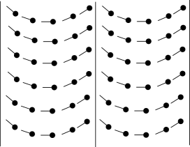
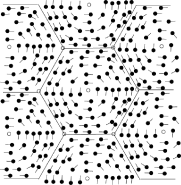
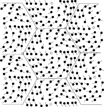
Chiral liquid crystals exhibit a variety of interesting phenomena Kamien . Chiral molecules tend to pack at a slight angle with respect to their neighbors. This preferred packing leads to spontaneous twist in the molecular orientation, producing phases such as the cholesteric and helically twisted smectic– (Sm–). In the case of two–dimensional Sm– films, the chiral modulation of the molecular orientation cannot occur in a defect–free fashion. Instead, for large chirality, the system will form a modulated phase consisting of a regular network of defect walls and possibly points. One possible modulated phase is a “striped” phase consisting of a regular array of parallel domain walls (Fig. 1). In between these walls the c director rotates in the sense preferred by the chirality. Another possible modulated phase consists of a hexagonal array of domain walls, with point defects located at the centers and corners of the hexagonal cells (Fig. 2).
Chirality also leads to unusual effects in orientationally disordered phases. As shown by Garoff and Meyer Garoff using symmetry arguments, if an electric field is applied to a system of chiral molecules in the Sm–A phase, an average molecular tilt will be produced, a response termed the electroclinic effect. These symmetry arguments do not, however, indicate the microscopic basis of the electroclinic effect. To date, two microscopic models have been proposed. In the first, the long axes of the molecules are assumed to be perpendicular to the smectic layers in the Sm–A phase. The electric field causes the molecules to tilt, with an accompanying significant change in the smectic layer spacing. In the second scenario suggested by de Vries deVries , the molecules in the Sm–A phase are assumed to be tilted even in the absence of the electric field, but azimuthally disordered. The electric field then induces azimuthal order, with no significant change in the smectic layer spacing. Experimental studies have shown evidence for both models, at least in terms of the field–induced layer contraction. Recently Selinger et al. Selinger noted that the optical birefringence of the liquid crystal will also distinguish between the two microscopic pictures. Because the field induces orientational order in the second model while simply tilting the already aligned molecules in the first, the birefringence should change dramatically in the former model, but not the latter. It appears that each of these models has experimental validity, namely there are materials with substantial layer contraction and weak field dependence in the birefringence, and other materials with the opposite properties. However, even a detailed theory based on the second model Selinger is unable to fully describe the experimental data. Furthermore, many materials show an unusually large electroclinic effect, well into the Sm–A phase. While it is tempting to associate this large effect with strong critical fluctuations Selinger , a completely different molecular mechanism may be relevant.
In this paper we propose a new model for the microscopic origin of the electroclinic effect, one that shares some of the macroscopic characteristics of the de Vries scenario, specifically, no layer contraction and field dependent birefringence. We postulate that what is assumed to be a Sm–A phase in some materials close to the Sm– transition, could in fact be a modulated version of the smectic– phase, a network of defects, walls and lines, but one where the spacing between the defects is in the subvisible range. This modulated phase would have no long–range azimuthal order or net polarization in the absence of an electric field. Thus, “to the eye”, this phase would appear to be a Sm–A phase. However, the application of an electric field distorts the structure of the defect array and leads to a large electroclinic effect. We now describe our proposed modulated phase and its response to an electric field in detail.
A bulk chiral Sm– can be described by the following elastic free energy deGennes :
| (1) | |||||
where is the projection of the nematic director on the plane of the layers. We assume that the molecular tilt is uniform and thus is assumed to be of fixed length. Chirality appears in two terms in this free energy. First, chirality induces a spontaneous twist of the director as indicated in the second term on the right hand side of Eq. (1), which is minimized in a helical state with pitch . Second, chirality induces spontaneous bend within each smectic layer as indicated by the last term in the free energy, where we assume . The free energy as written is zero for the perfect helical state with pitch . Because the smectic– phase is ferroelectric, with the spontaneous polarization perpendicular to , we must add to this free energy an electrostatic term arising from space charge density proportional to . We ignore this term for now, since we will find that in our proposed modulated phase, it adds only a constant to the free energy density, independent of the detailed structure of our model.
Considerable work has been done on analyzing Eq. (1) in two–dimensional chiral smectic liquid crystals, where the terms proportional to and in the free energy above are absent, and thus, there will be no competition between the two chiral terms. While only one chiral term is present, it is impossible to impose a spontaneous bend throughout the system. Defects must be introduced which separate domains of spontaneous bend, thus leading to a modulated phase. Two types of modulated phases have been proposed, a “striped” phase (Fig. 1) with a one–dimensional modulation Langer ; Petschek1 ; Petschek2 , and a hexagonal phase (Fig. 2) with a two–dimensional modulation. In the former case, parallel domain walls separate regions of spontaneous bend, while the latter consists of a two–dimensional array of domain walls and point disclinations. A point disclination lies at the center of each hexagonal cell, while the boundaries of the cell are domain walls where the director rotates by (a description of internal structures of these walls in terms of a nonfixed length director field is given in Petschek1 ; Petschek2 ). A point disclination is located at each corner of the cell. The hexagonal phase which involves nearly pure bend is favored over the striped phase when . The size of the unit cell is inversely proportional to the strength of the chirality parameter . The free energy of the hexagonal lattice includes (see Eq. (5) below) an attractive logarithmic interaction between the disclination at the center of the cell and the disclinations at the corners. Thus, strongly chiral materials, where the unit cell is small, will favor this interaction, and hence the hexagonal phase Kamien .
Returning to the full three–dimensional free energy, Eq. (1), we consider the possibility of a modulated phase. A bulk modulated phase must somehow compromise between the two competing chirality–induced tendencies: spontaneous in–layer bend and spontaneous twist about the layer normal. To describe the electroclinic effect in our proposed scenario the bulk modulated phase must have zero net polarization. Thus, a bulk modulated phase produced by simply extending the two–dimensional striped phase in the third direction is not acceptable, even if the pitch of the spontaneous twist were assumed to be infinitely large. A three–dimensional model for a thick chiral smectic film was proposed in Ref. Gorecka , where the in–plane modulation and domain walls are confined to surface regions, and the director twists in the interior of the film. Here we consider a space–filling modulated structure, with no need for surface structures.
Our starting point in constructing a suitable bulk modulated phase is the director configuration of the point disclination at the center of the two–dimensional hexagonal cell (Fig. 2). Expressing the director as , the angle is given by:
| (2) |
where the polar angle is given by , and (for the sign of the chirality appropriate to the structure shown in Fig. 2; for the opposite sign of chirality, , and the director circulation will be clockwise). This configuration represents pure bend and describes the director configuration away from the domain walls which bound the unit hexagonal cell. We now form a three–dimensional simple hexagonal lattice, with a unit cell of height , and cross–sectional area as in the two–dimensional case. We specify the director configuration as follows. In the midplane of the unit cell (taken to be the plane) we assume the perfect bend director configuration of Eq. (2). We then introduce twist in the direction, by writing the angle of the director as follows:
| (3) |
with
| (4) |
The pitch of this helical structure will be determined by minimizing the free energy density of the unit cell. With this model for the modulated phase, the and terms in the free energy, Eq. (1), can be combined into a term like the term with . We find that is so large that for simplicity we set .
Thus the unit cell has a disclination line running along the central axis of the cell and parallel disclination lines along the edges of the cell. Within the cell the director twists along the axis, in the sense preferred by the chirality (see Fig. 3). The top and bottom faces of the cell (perpendicular to the axis) are domain walls where the director undergoes a rotation by . The six other faces of the cell are walls where the director rotates by .
The free energy density of the hexagonal unit cell (of side ) relative to the helical state is given by:
| (5) |
where we have assumed that to simplify the elastic energy expression associated with the disclination lines. The core size of the disclination lines is denoted by , and we represent the domain wall energy per unit area of the top and bottom faces of the cell by , and the wall energy per unit area of each side face by . The term proportional to includes the elastic energy per unit cell associated with the disclination line at the center of the cell and the surrounding disclination Petschek2 . The term represents the remainder of the splay–bend elastic energy per unit cell. The term proportional to is obtained by integrating the corresponding term in Eq. (1) over the hexagonal unit cell using the director profile Eq. (3), thus ignoring the distortion of this profile near the edges of the cell.
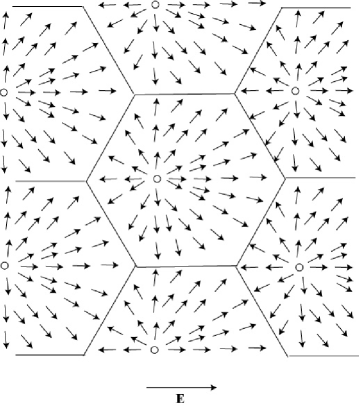
Before minimizing this free energy density we consider the response of the modulated state to an electric field, i.e., the electroclinic effect. We assume that the direction of the molecular dipole moment is given by . In the two–dimensional hexagonal modulated phase (see Fig. 2), the molecular dipole moments near the center of the cell will point radially outward, given the bend configuration of the director. Thus, an electric field applied in the direction will shift each disclination in the opposite direction, inducing a net polarization in the direction, as shown in Fig. 4.
For the three–dimensional cell we assume that the disclination lines at the cell centers also shift rigidly in the opposite direction to the field, ignoring any possible bending of the line due to the twist of the director in each cell (this should be a higher–order effect in the electric susceptibility). Assuming that the disclination lines shift by a distance in the direction, we find that the polarization (the net dipole moment of a cell divided by its volume ) is given to leading order in by:
| (6) |
where is the molecular dipole moment and is the average intermolecular spacing. In deriving we have assumed that the unit cell is a cylinder of radius centered on the original position of the line; ignoring the hexagonal shape of the cell merely changes the numerical prefactor appearing in the above expression.
The distance is determined by minimizing the change in the free energy density due to the presence of the field. Displacing the disclination line by a distance costs elastic energy proportional to . Thus, is given by:
| (7) |
the polarization by:
| (8) |
and the susceptibility by:
| (9) |
We now consider the minimization of , which is a function of and . Minimizing first with respect to , we find the following condition:
| (10) |
where
| (11) |
and
| (12) |
Eq.(10) has a solution for providing . This condition is physically equivalent Petschek1 to requiring that the domain wall energy of the side walls of the cell be negative in a non–fixed length director model, where the wall energy includes surface contributions, i.e., contributions from the total gradient term . Numerical minimization of the free energy density, Eq. (5), with respect to and , (choosing ) indicates that for values of that yield , (i.e., when the modulated state is favored over the helical state), , and:
| (13) |
The condition is sensible, because in that case the director pattern in each cell will be nearly pure bend. In this limit the condition implies that .
With very large, the polarization space charge density, proportional to varies in each cell as , with the distance from the central disclination, and is almost independent of . This produces an electric field which is almost purely radial, and constant in magnitude, considering the cell to be approximated by a cylinder. At the outer boundary of the cell there is a surface charge which precisely cancels the charge in the interior of the cell, so that there is no electric field outside each cell due to the charge distribution within the cell and on its boundaries. Thus the electrostatic energy density can be evaluated in a single cell, and is proportional to , independent of the radius or height of the cell. Although there are also ionic charges present in liquid crystals, typical estimates of their screening length indicate that they would not alter the electric fields at the length scales we are considering.
Assuming that is large, as indicated by the numerical minimization of Eq. (5), (specifically, ), and using Eq. (13), the free energy density Eq. (5) can be approximated as:
| (14) |
in which the electrostatic term, with spontaneous polarization density and dielectric constant , has been included.
We determine by numerically solving Eq. (10), using Eq. (13), and choosing and ; the results are shown in Fig. 5.
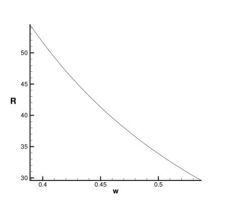
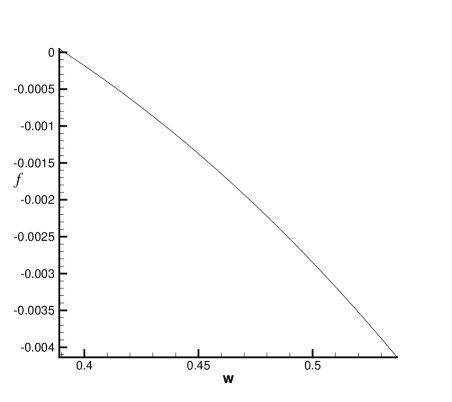
Using these results for we obtain the approximate free energy density, Eq. (14), as a function of (as shown in Fig. 6, choosing ). We see that if , the hexagonal phase is favored over the helical state. The numerical minimization of the full expression for the free energy, Eq. (5), indicates that in this phase , in units of an intermolecular spacing. Thus, the hexagonal phase in a real system would likely consist of a single lattice plane of hexagonal cells, i.e., the system is effectively two–dimensional.
II Conclusions
Returning now to the observations that motivated this work, we can see that if is a sub-visible length, then the modulated phase would resemble a Sm–A phase, optically. In our model, the apparent Sm–A to Sm– transition, as temperature is lowered, would actually be mimicked by the gradual change of physical parameters, so that below the transition temperature, the helical Sm– phase would have lower free energy than the modulated phase.
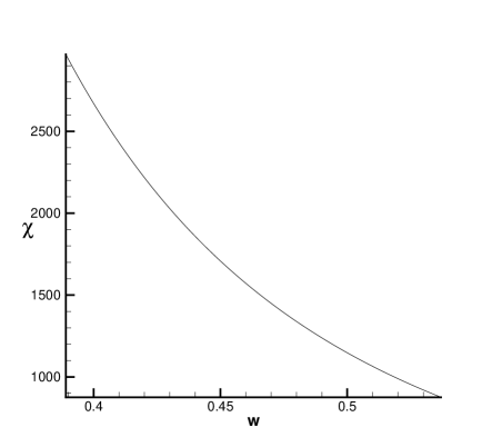
In our model, this would be a first order transition. Since the driving term in the free energy density, Eq. (5), favoring the modulated phase is the term proportional to , one could say that if decreases as temperature is lowered while all other parameters remain constant, then when passes through a particular value (about 0.39 in our calculated example) a first order transition to the helical Sm– phase would occur. Approaching this transition, would be increasing, as would the susceptibility, , as seen in the figures above.
The value of could well remain sub-visible throughout the range of the modulated phase. The electroclinic effect could be large throughout the temperature range of the modulated phase, with a rapid increase as the transition to the helical Sm– phase is approached. The mean smectic layer spacing would be almost constant through the phase transition. In the modulated phase it would be governed by an average between the layer spacing in the bulk and that in the side walls of the hexagonal cells, in which it is probably larger, due to a smaller molecular tilt angle. Therefore, at the phase transition, when the walls disappear, a very slight decrease in mean layer spacing would result. Qualitatively, these features agree with observations.
One could try to orchestrate a more physically appealing model of how the parameters of the free energy might change with temperature. For instance, steadily increasing would have essentially the same result as steadily decreasing. More generally, any combination of increasing and/or decreasing with falling temperature could produce the qualitative features of the apparent Sm–A phase and the phase transition.
The most valuable test for the validity of this model in real materials would be the direct observation of the periodic structure of the modulated phase. The first appropriate sub-optical probe that comes to mind is small angle X-ray diffraction, especially resonant X-ray diffraction that is most sensitive to variations of molecular orientation in a structure resonant . Hiroshi Yokoyama HY has pointed out to us that atomic force microscopy might also be a suitable probe, if the modulated phase structure is preserved in a thin layer deposited on a substrate.
Remarkably, in a recent paper bookshelf on one of the materials whose properties stimulated this work, optical observations consistent with a modulated phase, just at the transition from the Sm–A to the Sm– phase, are reported. In a thin layer of material in the “bookshelf” geometry, i.e., the smectic layers viewed edge-on, thin parallel stripes are observed running perpendicular to the smectic layers. These stripes are possibly consistent with the long thin hexagonal cells that we propose here.
Acknowledgments
We thank R. Pindak for helpful discussions. This work was supported by the National Science Foundation under grants DMR–9873849 and DMR–9974388.
References
- (1) For a recent review, see R. D. Kamien and J. V. Selinger, J. Phys.: Condens. Matter 13, R1 (2001).
- (2) S. Garoff and R. B. Meyer, Phys. Rev. Lett. 38, 848 (1977).
- (3) A. de Vries, A. Ekachai, and N. Spielberg, Mol. Cryst. Liq. Cryst. Lett. 49, 143 (1979); A. de Vries, Mol. Cryst. Liq. Cryst. Lett. 49, 179 (1979).
- (4) J. V. Selinger, P. J. Collings, and R. Shashidhar, Phys. Rev. E 64, 061705 (2001).
- (5) P. G. de Gennes and J. Prost, The Physics of Liquid Crystals (Clarendon Press, Oxford, 1993).
- (6) S. A. Langer and J. P. Sethna, Phys. Rev. A 34, 5035 (1986).
- (7) G. A. Hinshaw, R. G. Petschek, and R. A. Pelcovits, Phys. Rev. Lett. 60, 1864 (1988)
- (8) G. A. Hinshaw and R. G. Petschek, Phys. Rev. A 39, 5914 (1989).
- (9) E. Gorecka, M. Glogarová, L. Lejček, and H. Sverenyák, Phys. Rev. Lett. 75, 4047 (1995).
- (10) L.S.Matkin, S.J.Watson, H.F.Gleeson, R.Pindak, J.Pitney, P.Barois, A.M.Levelut, G. Srajer and J.Pollmann., Phys. Rev. E 64, 21705 (2001), L.S.Matkin, H.F.Gleeson, P.Mach, C.C.Huang, R.Pindak, G.Srajer, J.Pollmann, J.W.Goodby, M.Hird, and A.Seed, Appl. Phys. Lett. 76, 1863 (2000).
- (11) Private communication.
- (12) A.Tang, D.Konovalov, J.Naciri, B.R.Ratna, and S.Sprunt, Phys. Rev. E 65, 010703(R) (2002).