High-Frequency Impedance of Driven Superlattices
Abstract
The complex impedance of a semiconductor superlattice biased into the regime of negative differential conductivity and driven by an additional GHz ac voltage is computed. From a simulation of the nonlinear spatio-temporal dynamics of traveling field domains we obtain strong variations of the amplitude and phase of the impedance with increasing driving frequency. These serve as fingerprints of the underlying quasiperiodic or frequency locking behavior. An anomalous phase shift appears as a result of phase synchronization of the traveling domains. If the imaginary part of the impedance is compensated by an external inductor, both the frequency and the intensity of the oscillations strongly increase.
pacs:
72.20.Ht,73.61.-rSemiconductor superlattices (SL) show pronounced negative differential conductivity (NDC) [1]. If the total bias is chosen such that the average electric field is in the NDC region, stable inhomogeneous field distributions (field domains)[2] or self-sustained oscillations [3] with frequencies up to 150 GHz at room temperature[4] appear. Which of these scenarios occurs depends on bias, doping, temperature, and the properties of the injecting contact [5, 6, 7, 8, 9, 10]. For a recent overview see Ref. [11].
In order to apply the self-sustained oscillations as a high–frequency generator in an electronic device, it is crucial to know the response of the SL in an external circuit. A key ingredient for the analysis is the complex impedance of the SL in the respective frequency range. This is the subject of this paper where the complex impedance is evaluated numerically by imposing an additional ac bias to the SL. The interplay of the self-sustained oscillations and the external frequency causes a variety of interesting phenomena such as frequency locking, quasi-periodic and chaotic behavior which has been extensively studied both theoretically [12, 13, 14] and experimentally [15, 16]. In contrast to those studies we focus on the response to the circuit and concurrent phase synchronization phenomena in this work.
We describe the dynamical evolution of the SL by rate equations for the electron densities in the quantum wells, together with Poisson’s equation for the electric fields. The current densities between adjacent quantum wells are evaluated within the model of sequential tunneling, and Ohmic boundary conditions with a contact conductivity are used. For details see Refs. [10, 11]. Here we apply a periodic bias signal and study the total current . In particular we consider the Fourier component which gives the complex impedance
| (1) |
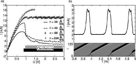
As an example we consider the SL structure studied in Ref. [16]. It consists of GaAs wells of width 4.9 nm separated by 1.3 nm AlAs barriers. The sample is n-doped with a density of per period and the sample cross section is . We estimate the energy broadening meV, which effectively gives the sum of phonon, impurity and interface roughness scattering rates. All calculations are performed at room temperature.
In Fig. 1a we display the calculated current–voltage characteristic for . While for large values of the contact conductivity stationary field domains occur, self-sustained current oscillations (where pairs of accumulation and depletion fronts travel through the sample) are found for lower (Fig. 1b). This scenario is quite general for moderately doped samples [7, 11]. In the following we use A/Vm giving best agreement with the measured current-voltage characteristic.
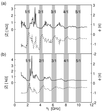
At V, the self-sustained oscillations exhibit a frequency of GHz. Now we study the change in the current signal by imposing an additional ac-bias amplitude with frequency . Fig. 2 displays the absolute value and the phase of the complex impedance given by Eq. (1). For both strengths of the ac amplitude one observes strong variations in the amplitude and phase of . In particular one observes pronounced minima in and a corresponding monotonic increase in around frequencies which are approximately integer multiples of . This is due to frequency locking [17], where the external frequency modifies the main oscillation frequency to such that is a rational number. While locking occurs in a rather wide frequency range for , locking into rational numbers with larger denominators are less easy to observe (The corresponding widths of the locking intervals roughly follow the position in the Farey-tree of the rational numbers, see [17]. The width of the locking ranges also increases with .) A more detailed examination indicates that the local minima in correspond to the locking regions, and increases with in those intervals, while a decrease is frequently observed outside these ranges where quasi-periodic or possibly chaotic behavior occurs. Thus the presence of several locking intervals[16] explains the variety of peaks.
For high frequencies the variations of become less pronounced and and is observed. This corresponds to a capacitive current with an effective frequency-dependent capacitance . At GHz this gives fF. This capacitance results from the interaction with the internal front dynamics in the SL structure; the intrinsic sample capacitance fF is significantly smaller.
While we have only shown results for V and A/Vm here, we checked that the features discussed above neither change for different biases nor different contact conductivities, albeit the main oscillation frequency and the locking ranges change slightly.
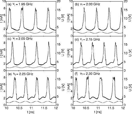
Now we focus on the 1/1 locking region which is of interest if the device is used as an oscillator. In Fig. 3 we show the current and bias signal for different frequencies . In parts (a) ( GHz) and (f) ( GHz) no complete locking occurs and the current does not exhibit a periodic signal. Between these frequencies the current signal is periodic with a frequency imposed by the external bias. While the current peaks occur around the minima of the external bias for GHz (corresponding to ), the delay between the current peaks and the bias maxima decreases with frequency until they are approximately in phase at the upper boundary of the locking range at GHz (corresponding to ). It is intriguing to note that this behavior is opposite to the response of a damped linear oscillator, where the phase between the driving signal and the response shifts from to with increasing driving frequency. The current peaks correspond to the formation of a domain at the emitter, while during the current minima the domain traverses the sample. The domain transit velocity is larger for smaller voltage. The phase shift between current and voltage adjusts such that the domain velocity increases with increasing driving frequency during the whole locking interval. This is a phase synchronization effect induced by the domain dynamics.
Let us analyze the behavior close to the onset of the locking interval in detail, see Fig. 4. The main frequency component of the current signal is given by . In the locking region it is equal to the frequency of the driving bias such that vanishes in a finite range of . In contrast, far away from the locking is essentially given by the free oscillation frequency , thus exhibits a linear relation. Close to the boundaries of the locking region a square root behavior can be detected, which is a general feature of frequency locking, see, e.g., [18].
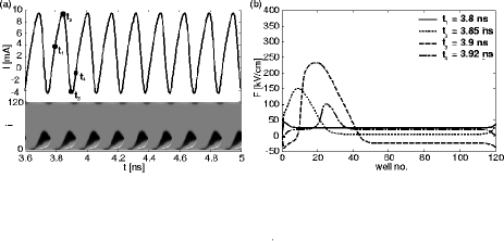
Fig. 4b shows the amplitude and the monotonically increasing phase of the impedance over the whole locking interval. We extract an impedance for . Now we compensate this impedance by an external circuit with an inductor of nH and a resistor of 25 in series with the SL. (The resistor may result both from connecting wires or due to radiation damping in a real device.) Fig. 5 shows that the oscillation mode is strongly affected: The frequency is increased to GHz, the oscillation is more sinusoidal, and the current amplitude increases. Thus the device performance of the SL is strongly improved. This effect is due to a different oscillation mode, where the domains are quenched such that they only traverse a small part of the SL. As the domain velocity is almost constant, the frequency increases.
We have shown that the amplitude and the phase of the complex impedance exhibit strong variations with the driving frequency . The distinct minima of the amplitude of the impedance correspond directly to the frequency locking intervals. In these regions the frequency components of the current at are particularly large, leading to small . The phase of the impedance is monotonically increasing with frequency from to zero in the locking intervals, which constitutes a phase shift of compared to the standard behavior of a driven oscillator. These effects are caused by phase synchronization of the spatio-temporal dynamics of the traveling field domains in the NDC regime. Compensating the imaginary part of the impedance in an external circuit strongly improves the device performance of the SL.
Partial support from Sfb 555 is acknowledged.
REFERENCES
- [1] L. Esaki and R. Tsu, IBM J. Res. Develop. 14, 61 (1970).
- [2] L. Esaki and L. L. Chang, Phys. Rev. Lett. 33, 495 (1974).
- [3] J. Kastrup, R. Klann, H. T. Grahn, K. Ploog, L. L. Bonilla, J. Galán, M. Kindelan, M. Moscoso, and R. Merlin, Phys. Rev. B 52, 13761 (1995).
- [4] E. Schomburg, R. Scheurer, S. Brandl, K. F. Renk, D. G. Pavel’ev, Y. Koschurinov, V. Ustinov, A. Zhukov, A. Kovsh, and P. S. Kop’ev, Electronics Letters 35, 1491 (1999).
- [5] A. Wacker, M. Moscoso, M. Kindelan, and L. L. Bonilla, Phys. Rev. B 55, 2466 (1997).
- [6] M. Patra, G. Schwarz, and E. Schöll, Phys. Rev. B 57, 1824 (1998).
- [7] D. Sánchez, M. Moscoso, L. L. Bonilla, G. Platero, and R. Aguado, Phys. Rev. B 60, 4489 (1999).
- [8] J. Wang, B. Q. Sun, X. Wang, Y. Wang, W. Ge, and H. Wang, Appl. Phys. Lett. 75, 2620 (1999).
- [9] H. Steuer, A. Wacker, E. Schöll, M. Ellmauer, E. Schomburg, and K. F. Renk, Appl. Phys. Lett. 76, 2059 (2000).
- [10] A. Amann, A. Wacker, L. L. Bonilla, and E. Schöll, Phys. Rev. E 63, 066207 (2001).
- [11] A. Wacker, Phys. Rep. 357, 1 (2002).
- [12] O. M. Bulashenko and L. L. Bonilla, Phys. Rev. B 52, 7849 (1995).
- [13] J. C. Cao and X. L. Lei, Phys. Rev. B 60, 1871 (1999).
- [14] D. Sánchez, G. Platero, and L. L. Bonilla, Phys. Rev. B 63, 201306 (2001).
- [15] Y. Zhang, J. Kastrup, R. Klann, K. Ploog, and H. T. Grahn, Phys. Rev. Lett. 77, 3001 (1996).
- [16] E. Schomburg, K. Hofbeck, R. Scheurer, M. Haeussler, K. F. Renk, A.-K. Jappsen, A. Amann, A. Wacker, E. Schöll, D. G. Pavel’ev, and Y. Koschurinov, Phys. Rev. B submitted (2002).
- [17] H. G. Schuster, Deterministic Chaos, 2 ed. (VCH Verlagsgesellschaft, Weinheim, 1988).
- [18] J. Peinke, J. Parisi, O. Rössler, and R. Stoop, Encounter with Chaos (Springer, Berlin, Heidelberg, 1992).