Superconducting energy gap distribution in MgB2 \sodtitleSuperconducting energy gap distribution in c-axis oriented MgB2 thin film from point contact study \rauthorYu. G. Naidyuk, I. K. Yanson, L. V. Tyutrina et al. \sodauthorYu. G. Naidyuk+, I. K. Yanson+, L. V. Tyutrina+ et. al. \dates15 January 2002*
Superconducting energy gap distribution in c-axis oriented MgB2 thin film from point contact study
Abstract
We have analyzed about hundred voltage-dependent differential resistance curves of metallic point contacts between -axis oriented MgB2 thin film and Ag, which exhibit clear Andreev reflection features connected with the superconducting gap. About one half of the curves show the presence of a second larger gap. The histogram of the double gap distribution reveals distinct maxima at 2.4 and 7 meV, while curves with a single-gap features result in more broad maximum at 3.5 meV. The double-gap distribution is in qualitative agreement with the distribution of gap values over the Fermi surface calculated by H. J. Choi et al. (cond-mat/0111183). The data unequivocally show the presence of two gaps meV and meV in MgB2 with gap ratio . Our observations prove further a widely discussed multigap scenario for MgB2, when two distinct gaps are seen in the clean limit, where a single averaged gap is present in the dirty one.
73.40.Jn, 74.76Db, 74.80.Fp
Introduction. Direct spectroscopic investigations of the superconducting order parameter in recently discovered [1] superconductor MgB2 with T40 K by tunneling [2, 3, 4, 5, 6, 7, 8, 9, 10] and point-contact spectroscopy [10, 11, 12, 13, 14, 15, 16, 17] show unambiguously an energy gap in the quasiparticle density of states (DOS). However, the experimental results are controversial as to the gap width , whose variation from 1.5 to 8 meV (see, e. g., review [18]) is unexpectedly large, pointing to the possibility of multiphase or nonhomogeneous samples, degraded surface, or anisotropic energy gap. Another way to solve this puzzle is to consider two superconducting gaps in MgB2, as proposed by Liu et al. [19], accounting complex electronic structure of MgB2 with both quasi-2D and 3D Fermi surface [20]. Indeed, several papers [6, 7, 8, 15, 16, 17] have reported double gap structure in the differential conductance (resistance) with the smaller gap being far below weak-coupling BCS value =1.76kBT6 meV and the larger gap slightly above the standard BCS one, in accordance with theory [19].
Therefore, one of the intriguing key issues of superconducting state of MgB2 is whether the double gap state is intrinsic or the spread of the gap values is a result of anisotropy, nonhomogeneity, surface effect, etc. In other words, before macroscopic high quality single crystals will be available for thorough investigations, the sample imperfection may raise doubts about the final conclusion. However, in our mind, good reproducibility of the double-gap values given by different authors [6, 7, 8, 15, 16, 17] by different, in their physical background, methods such as tunneling and point-contact spectroscopy carried out on different samples such as pellets, films, grains, all this with a great degree of probability supports intrinsic nature of the double gap in MgB2.
In this paper we will give further confirmation of double gap scenario in MgB2 based on analysis of about hundred point-contact spectra of c-axis oriented thin films.
Experimental and calculation details. We have measured the high-quality c-axis oriented 0.4 m thick MgB2 film [21] grown by a PLD technique on Al2O3 substrate. The resistivity of the film exhibits a sharp transition at 39 K with a width of 0.2 K from 90% to 10% of the normal state resistivity [21]. The residual resistivity at 40 K is 6 cm 111There is a scattering by factor of 4 in for the different films. and RRR=2.3.
Different point contacts (PCs) were established in situ directly in liquid 4He by touching as-prepared surface (sometimes etched by 1% HCl solution in ethanol) of the MgB2 film by a sharpened edge of an Ag counterelectrode, which were cleaned by chemical polishing in HNO3. This geometry corresponds to the current flowing preferably along the c axis. A number of contacts were measured by touching of the film edge after breaking Al2O3 substrate. By this means, the current flows preferably along the ab plane. The differential resistance dd vs was recorded using a standard lock-in technique. The normal resistance (at ) of investigated contacts ranged mainly between 10 and 1000 at 4.2 K.
The important characteristic of PC is their size or diameter , which can be determined from the simple formula derived by Wexler [22] for contact resistance:
| (1) |
where two terms represent ballistic Sharvin 222In the case of interface scattering Sharvin resistance should be multiple by factor (1+Z2)[24]. and diffusive Maxwell resistance, correspondingly. Here e2, where is the Fermi momentum and is the density of charge carriers. The latter for MgB2 is estimated at [23], which results in cm2 using cm/s [20]. Hence, the upper limit for elastic mean free path for our film is about 3 nm. In this case, according to Eq. (1), the condition is fulfilled for PC with or for lower resistance supposing multiple contacts in parallel.
We have utilized generally used Blonder-Tinkham-Klapwijk equations [24] describing characteristic of ballistic N-c-S metallic junctions (here N is normal metal, c is constriction and S is superconductor) by accounting for the processes of Andreev reflection. At finite barrier strength at the N-S interface characterized by parameter and , the theory gives the dd curves with minima at e. To get the correct , the fit of the measured curves to the theory should be done. The additional smearing of dd curves due to, e. g., broadening of the quasiparticle DOS in the superconductor can be taken into account by including parameter [25].
In the case of curves with double gap structure we calculated, according to the theory [24], the sum of two differential conductances dd with the weight for the larger gap and, correspondingly, with for the smaller one. After this, we have transformed dd into d/d to compare with the measured dependences. The best fit was achieved, as a rule, by using its own values of and for large and small gap. It is acceptable if we suppose that we have a number of microconstrictions with various in the region of mechanical touch. It is worthy to note that, with increasing of weight factor, the difference between and values for large and small gap becomes smaller or even vanishes for some PCs.
Results and discussion. Approximately one half (44 of total 91) of analyzed raw d/d vs. curves show visible two-gap structure, although, in most cases with shallow features corresponding to a larger gap. The samples of some dd curves taken at 4.2 K with double-gap structure, along with calculated curves, are shown in Fig. 1. In spite of a number of fitting parameters (, , , ) for curves with pronounced (or at least visible as shown in Fig. 1) double gap features determined and are robust as to fitting procedure.
It turns out that histogram of gaps distribution built on the basis of fitting of 44 spectra (see Fig. 2a) has two well-separated and quite narrow (especially for the small gap) maxima.
The double-gap distribution is in qualitative agreement with the distribution of gap values over the Fermi surface recently calculated in [26] (see Fig. 2c). The main difference is that theoretical distribution for lower gap is wider and has a dominant maxima around 1.6 meV. This discrepancy can be resolved when we draw attention that we have measured curves with double gap structure for contacts that is predominantly along the c-axis. In this case, according to [26], gap values along c-axis spreads between 2 and 3 meV. The c-axis directionality of our measurements is, apparently, the main reason of a shallow large gap structure in d/d, because large gap dominates in the ”a-b” plane [26].
It should be mentioned that two very different order parameters exist only in the clean limit . Since in our case has upper limit in 3 nm and the coherence length 5 nm [27], the observation of two gaps is in line with our supposition that in the PC area there are small grains with a much larger mean free path. Indeed, SEM image of MgB2 films [16] shows that the film is granular with 100-500 nm large grains. Therefore, in the area of mechanical contact there are some amount of small metallic bridges, perhaps, with slightly different crystallographic orientation being in parallel.
The single gap is seen for the dirty limit 333On dd of ”edge” contacts (a total of 11 curves) only single gap structure was observed, probably due to the deterioration of the film edge after breaking. and is average of small and large gaps with some weights. If we assume that this weight has some relation to the weight used in the fitting procedure, then, admittedly, =3.4 meV by using upper limit 0.2 (see Fig. 3). This agrees with the position of the maximum of single-gap distribution at 3.5 meV (see. Fig. 2b). By the way, according to the calculation in [28], a large amount of impurity scattering will cause the gaps to converge to 4.1 meV.
Therefore the superconducting properties of this compound can be strongly influenced by nonmagnetic defects and impurities, which seem to have a great impact also on the scattering of gap value(s) given by different authors.
As to factor it is hardly to see in Fig. 3 its dependence on or PC size, which one would expect if small gap reflects a degraded surface or large gap is a result of surface states [29].
Table II shows double gap values given by different authors. A quite good correspondence between our results and data of other authors carried out on different types of MgB2 samples is evident. In our case averaged over 44 curves, the ratio of the larger gap to the lower one 2.850.15 is close to the theoretical value 3:1 [19].
In conclusion. We have analyzed d/d point-contact spectra of MgB2 with clear single- and double-gap structure. The observed distinct maxima in the double gap distribution which is consistent with theoretical calculations [26] ruled out surface or multiphase origin of gap structure and testify about intrinsic superconducting double-gap state in MgB2. The averaged gap value ratio turned out to be in accordance with the theoretically predicted ratio 1:3 [19].
Acknowledgments The work in Ukraine was supported by the State Foundation of Fundamental Research, Grant 7/528-2001. The work at Postech was supported by the Ministry of Science and Technology of Korea through the Creative Research Initiative Program. IKY is grateful to Forschungszentrum Karlsruhe for hospitality.
References
- [1] J. Nagamatsu, N. Nakagawa, T. Muranaka et al., Nature 410 63 (2001).
- [2] G. Karapetrov, M. Iavarone, W. K. Kwok et al., Phys. Rev. Lett. 86 4374 (2001).
- [3] G. Rubio-Bollinger, H. Suderow, S. Vieira, Phys. Rev. Lett. 86 5582 (2001).
- [4] A. Sharoni, I. Felner, D. Millo, Phys. Rev. B 63 220508R (2001).
- [5] P. Seneor, C.-T. Chen, N.-C. Yeh et al., Phys. Rev. B 65 012505 (2002).
- [6] F. Giubileo, D. Roditchev, W. Sachs et al., cond-mat/0105146.
- [7] F. Giubileo, D. Roditchev, W. Sacks et al., Phys. Rev. Lett. 87 177008 (2001).
- [8] Mohamed H. Badr, Mario Freamat, Yuri Sushko, and K.-W. Ng, cond-mat/0110421.
- [9] Y. Zhang, D. Kinion, J. Chen et al., cond-mat/0107478.
- [10] H. Schmidt, J. F. Zasadzinski, K. E. Gray et al., Phys. Rev. B 63 220504(R) (2001).
- [11] A. Kohen and G. Deutscher, Phys. Rev. B 64 060506(R) (2001).
- [12] A. Plecenik, Š. Beňačka, P. Kúš et al., Physica C, 368 251 (2002).
- [13] F. Laube, G. Goll, J. Hagel et al., Europhysics Lett. 56 296 (2001).
- [14] R. S. Gonnelli, A. Calzolari, D. Daghero et al., cond-mat/0107239.
- [15] P. Szabó, P. Samuely, J. Kacmarćik et al., Phys. Rev. Lett. 87 137005 (2001).
- [16] Y. Bugoslavsky, Y. Miyoshi, G. K. Perkins et al., cond-mat/0110296.
- [17] N. L. Bobrov, P. N. Chubov, Yu. G. Naidyuk et al., cond-mat/0110006.
- [18] C. Buzea and T. Yamashita, Superconductors, Science & Technology, 14 N11, R115-R146, (2001).
- [19] A. Y. Liu, I. I. Mazin, and J. Kortus, Phys. Rev. Lett. 87 087005 (2001).
- [20] J. Kortus, I. I. Mazin, K. D. Belashchenko et al., Phys. Rev. Lett. 86 4656 (2001).
- [21] W. N. Kang, Hyeong-Jin Kim, Eun-Mi Choi et al., Phys. Rev. Lett. 87 087002 (2001).
- [22] A. Wexler, Proc. Phys. Soc. 89 927 (1966).
- [23] P. C. Canfield, D. K. Finnemore, S. L. Bud’ko et al., Phys. Rev. Lett. 86 2423 (2001).
- [24] G. E. Blonder, M. Tinkham, T. M. Klapwijk, Phys. Rev. B 25 4515 (1982).
- [25] R. C. Dynes, V. Narayanamurti and J. P. Garno, Phys. Rev. Lett. 41 1509 (1978).
- [26] Hyoung Joon Choi, David Roundy, Hong Sun et al., cond-mat/0111183.
- [27] D. K. Finnemore, J. E. Ostenson, S. L. Bud’ko et al., Phys. Rev. Lett. 86 2420 (2001).
- [28] A. Brinkman, A. A. Golubov, H. Rogalla et al., cond-mat/0111115.
- [29] V. D. P. Servedio, S.-L. Drechsler, T. Mishonov, cond-mat/0111434.
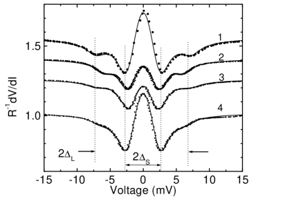
Reduced differential resistance d/d vs. measured at T = 4.2 K for four MgB2-Ag contacts with double gap structure (symbols). Thin lines are theoretical dependences calculated with parameters given in the Table I. The curves (1-3) are vertically offset for clarity. Vertical dashed lines show approximately position of large and small gaps. Experimental curves are taken nominally in c-directions
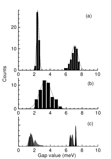
The superconducting energy-gap distribution in c-axis-oriented MgB2 thin film in the case: (a) double gap and (b) single gap. Thin lines show Gaussian fit with maxima at (a) 2.45 and 7 meV and (b) 3.5 meV. The histogram window of 0.25 meV for (a) and 0.5 meV for (b) is chosen to get the most close to normal (Gaussian) distribution. (c) Distribution of gap values over the Fermi surface calculated in [26]
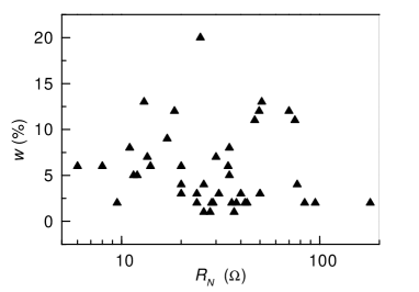
Dependence of the weight factor on the point-contact resistance
| Parameters | Curve 1 | Curve 2 | Curve3 | Curve 4 |
|---|---|---|---|---|
| RN, | 47 | 35 | 20 | 34 |
| , meV | 7.4 | 6.25 | 7.35 | 7.3 |
| , meV | 2.6 | 2.54 | 2.4 | 2.6 |
| -factor | 0.11 | 0.08 | 0.07 | 0.06 |
| ZL | 0.7 | 0.71 | 0.63 | 0.21 |
| ZS | 0.75 | 0.55 | 0.56 | 0.76 |
| , meV | 0.4 | 0.1 | 0.55 | 0 |
| , meV | 0.5 | 0.54 | 0.38 | 0.3 |