Current address: ]Cielo Communications, Inc., 325 Interlocken Parkway, Broomfield, CO 80021.
Charge Transport Processes in a Superconducting Single-Electron Transistor Coupled to a Microstrip Transmission Line
Abstract
We have investigated charge transport processes in a superconducting single-electron transistor (S-SET) fabricated in close proximity to a two-dimensional electron gas (2DEG) in a GaAs/AlGaAs heterostructure. The macroscopic bonding pads of the S-SET along with the 2DEG form a microstrip transmission line. We observe a variety of current-carrying cycles in the S-SET which we attribute to simultaneous tunneling of Cooper pairs and emission of photons into the microstrip. We find good agreement between these experimental results and simulations including both photon emission and photon-assisted tunneling due to the electromagnetic environment.
Charge transport in all-superconducting single-electron transistors (S-SETs) has been studied in detail, and numerous current-carrying cycles have been identified, including the Josephson-quasiparticle (JQP) cycle,Fulton et al. (1989); Maassen van den Brink et al. (1991a); Nakamura et al. (1996, 1997) the 3 cycleHadley et al. (1998) and Andreev reflection.Fitzgerald et al. (1998) What processes occur in a given S-SET is determined by a complex interplay between Cooper pair tunneling and charging effects, leading to rich behavior in S-SET current-voltage characteristics. Further complexity is added by the electromagnetic environment, which can cause photon-assisted tunneling (PAT) of quasiparticlesMartinis and Nahum (1993); Hergenrother et al. (1994) and incoherent tunneling of Cooper pairs.Maassen van den Brink et al. (1991b); Siewert and Schön (1996) Experiments have addressed the influence of the environment on a variety of tunnel junction systems, including electron pumps,Martinis and Nahum (1993); Covington et al. (2000) single tunnel junctions,Holst et al. (1994) Josephson junction arraysRimberg et al. (1997) and S-SETs fabricated above a ground plane, focusing on the supercurrent.Kycia et al. (2001) The effect of the environment on S-SETs remains interesting given the potential use of Coulomb blockade devices for quantum computation.Nakamura et al. (1999) Here we report measurements on samples similar to that in Ref. Kycia et al., 2001, but focus on transport at higher biases. We observe previously unreported charge transport cycles which we attribute to Cooper pair tunneling with simultaneous emission of a photon into the environment. We find good agreement between our measurements and simulations based on the orthodox theory of electron tunneling,Likharev (1988); Grabert and Devoret (1992) including the effects of both photon emission and PAT.
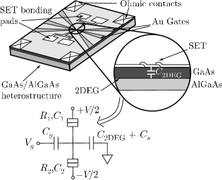
Our samples consist of Al/AlOx/Al S-SETs fabricated on a GaAs/AlGaAs heterostructure containing a two-dimensional electron gas (2DEG) located below the substrate surface, as illustrated in Fig. 1. The heterostructure, grown on a GaAs substrate using molecular beam epitaxy, consists of the following layers: of GaAs, of Al0.3Ga0.7As and of GaAs. The Al0.3Ga0.7As is delta-doped with Si from the lower GaAs/Al0.3Ga0.7As interface, at which the 2DEG forms. The SETs are fabricated using electron-beam lithography and shadow evaporation techniques. The central island of the SET is coupled by a capacitance to the 2DEG beneath it, which is held at ground. The SET is surrounded by six Au gates, as described elsewhere.Lu et al. (2000)
We model the SET as shown, with tunnel junction resistances and capacitances and respectively. A voltage applied to one of the Au gates is used to adjust the electrostatic potential of the SET island through the capacitance . The remaining gates are held at ground and contribute to the total island capacitance . We focus first on the 2DEG far from the SET, which in conjunction with the macroscopic bonding pads forms a microstrip transmission line to which the SET is coupled. Such microstrip can resonate at microwave frequencies and thereby affect transport in tunnel junction systems.Holst et al. (1994); Kycia et al. (2001) We have examined two such samples with junction resistances ranging from to , and a third control sample fabricated on a piece of GaAs without a 2DEG. Sample parameters are given in Table 1 below.
The large value of () for Sample 1 (2), along with the total gate capacitance helped ensure that the charging energy satisfied where is the superconducting gap. For the control sample, and were sufficiently large to give a comparable . For all the samples, the Josephson energy given by the Ambegaokar-Baratoff relationAmbegaokar and Baratoff (1963) satisfied so that the charge state of the island is well defined, justifying use of the orthodox theory. We define the charging energy of the SET , where is the offset charge induced by the gate voltage. At low temperatures, electrons will tunnel through a given junction only when the change in free energy , including both changes in and work performed by the bias voltage . For single-electron tunneling is in general forbidden by the combined effects of the Coulomb blockade and the superconducting gap, though more complex charge transport processes such as the JQP and 3 cycles are allowed at specific locations in the - plane.
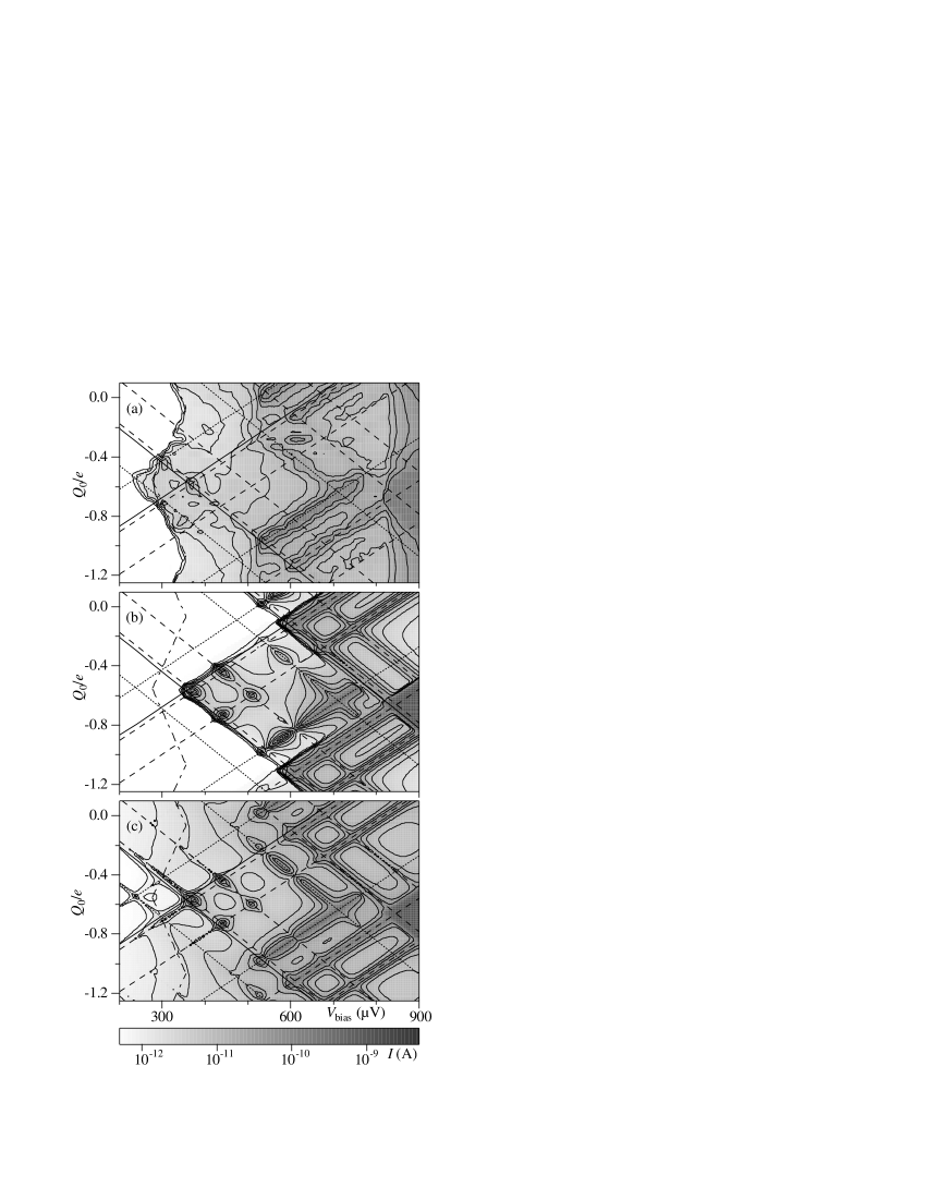
We measured the samples in a dilution refrigerator at using a four probe configuration symmetrically biased with respect to ground. High-frequency noise was excluded using standard techniques as described elsewhere.Lu et al. (2000) Sample parameters such as the capacitances and summed junction resistances were determined from the measurements. The resistance ratio was chosen to give the correct relative size of features associated with each junction in the simulations. Current was measured versus bias voltage for a series of different values of the offset charge for all three samples; results for Sample 1 are presented in Fig. 2(a).
| Sample | ||||||
|---|---|---|---|---|---|---|
| 1 | 207 | 181 | 120 | 118 | ||
| 2 | 201 | 375 | 260 | 77 | ||
| control | 198 | 515 | 322 | 91 |
Several resonances are visible for voltages between 500 and . The most pronounced are the usual JQP peaks, some of which are paralleled by two smaller resonances. We believe these additional resonances are analogs of the usual JQP peaks, but differ in that Cooper pairs emit one or more photons into the transmission line while tunneling. We refer to them as JQP-ph peaks. Several smaller features are also visible near at biases between 300 and . To support our interpretation of the JQP-ph resonances, and to identify the smaller features, we begin with conservation of energy, including not only the usual terms accounting for creation of quasiparticles and changes in charging energy,Fitzgerald et al. (1998); Pohlen (1999) but also a term allowing for emission of photons:
Here is the fraction of the bias voltage available across junction and the number of electrons transferred across it, is the change in the island charge, is the number of quasiparticles created, and is the number of photons of energy emitted. The proper choice of , , and , gives transition rules for quasiparticle, Cooper pair, Cooper pair with photon emission, and 3 tunneling processes. These are indicated schematically in Fig. 3, and transition lines corresponding to them are shown in Fig. 2.
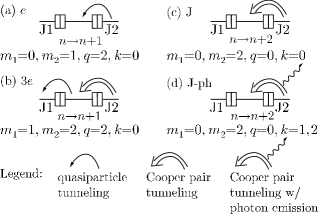
The JQP features in Fig. 2(a) lie along Cooper pair transition lines, either with (J-ph) or without (J) photon emission, since Cooper pair tunneling is a resonant process. For the primary () JQP peak between and , the cycle begins with a Cooper pair transition through J1 (), followed by successive quasiparticle transitions through J2 ( and ) which return the island to its original charge state and allow the cycle to begin again. As it must, the JQP peak begins just above the quasiparticle line for the transition, which gives the requirement .
To address the JQP-ph peaks, the fundamental frequency for photon emission was determined by adjusting so that a one-photon J-ph line coincided with the first JQP-ph resonance between and . Best results were obtained for . For Cooper pair tunneling with we obtain the condition , in good agreement with the observed location of the resonance. Since the typical lead width () for the pad structures is much greater than the 2DEG depth of , the effective wavelength for excitations on the microstripPozar (1998) is where is the dielectric constant of GaAs. The fundamental resonance corresponds to a length , in agreement with the known dimensions of our lead structures. Resonances with a best fit for were observed in Sample 2, while none were observed in the control sample, supporting our interpretation of the data. The position of the J-ph line does not match well to that of the associated resonance, perhaps not surprising given its small size and the large background current.
To gain further insight into the features in Fig. 1(a), we turn to our simulations. Here, to account for the JQP-ph resonances, we make a phenomenological modification of the theory of Averin and AleshkinAverin and Aleshkin (1989); Aleshkin and Averin (1990) and write for the Cooper pair tunneling rate
| (2) |
where is the change in free energy due to the tunneling of the Cooper pair and is the rate of the first subsequent quasiparticle tunneling. The were chosen as (giving the usual Averin-Aleshkin term) and , the weightsGrabert and Devoret (1992) for independent emission of photons into a single mode.111While this approach gives reasonable agreement with the measured peak heights, the JQP-ph features may in fact be due to harmonics of the stripline resonance. None of our main conclusions are affected, however, by whether the higher J-ph resonances are due to single or multiple photons.
Results of a simulation including the effects of photon emission are shown in Fig. 2(b). The agreement is reasonable, especially at higher biases, where the and 2 JQP-ph lines appear. Moreover, the simulation predicts the appearance of a feature at the intersection of the J-ph lines for J1 and J2 near and . A corresponding peak can also be seen in the data in Fig. 2(a). This feature is an analog of the peakHadley et al. (1998) but with Cooper pair tunneling replaced by J-ph processes, and we refer to it as the 3-ph peak. Our samples do not satisfy the condition for the appearance of the usual 3 cycle. The corresponding condition for the 3-ph cycle in Sample 1 is which is just satisfied. A similar feature appears in the data (at and ) near the intersection of a J-ph line for J1 and a J-ph line for J2. A corresponding peak appears at the same location in the simulation.
Despite this level of agreement, some discrepancies exist. The measured current remains substantial down to the 3 threshold line between 275–, while the calculated current in Fig. 2(b) nearly vanishes for all below the 3-ph peak. Furthermore, in the simulation the primary () JQP peak is strongly suppressed at the intersections with J-ph transition lines; an example occurs in Fig. 2(b) at and where the primary JQP peak for J1 intersects a line for J2. The standard JQP process would begin with the Cooper pair transition . Our simulations indicate that at this intersection the J-ph transition is allowed, and is followed rapidly by a quasiparticle transition. The transition is allowed but slow, so that the occupational probability of the state is quite small (), and the JQP cycle is suppressed. There is, however, no clear sign of suppression of the primary JQP cycle in our data.

We can account for these discrepancies to some extent by considering PAT due to the environment, here assumed to be the 2DEG in the immediate vicinity of the SET. Since the effective environment temperature can be much larger than the SET electron temperature,Martinis and Nahum (1993) PAT can be quite significant. Following Siewert and Schön,Siewert and Schön (1996) we incorporate it into our calculation by adding the rate
| (3) |
to all quasiparticle tunneling events for which . Fig. 2(c) shows the results of a simulation including PAT with much improved agreement. Appreciable current appears at voltages around the 3 threshold lines.
In addition, the suppression of the JQP peak at intersections with J-ph lines is largely lifted. This can be seen in greater detail in Fig. 4 which shows the calculated vs. for , both with and without PAT. The inclusion of PAT increases the primary JQP peaks for both J1 and J2. In the inset, we make a comparison with data from Sample 1 at , a voltage below the cutoff for the JQP-ph cycle, so that only the JPQ peak is visible. The JQP peaks for both J1 and J2 are near J-ph transition lines here, and in the absence of PAT the simulation underestimates the actual JQP current. Addition of PAT brings the simulation in much closer agreement with the data, although it does not correctly predict the width of the JQP peak, a topic which will be addressed in a separate publication.
In conclusion, we have investigated charge transport processes in an S-SET which is coupled to a 2DEG, so that the contact pad structures form microstrip resonators. We have observed current-carrying cycles which involve tunneling of a Cooper pair and simultaneous photon emission, including JQP-ph and 3-ph processes. Simulations performed using the orthodox theory agree well with the data, particularly when the effects of PAT due to the environment are included. In the simulations, suppression of the primary JQP in the vicinity of J-ph lines is partially lifted by the effects of PAT. While we do not observe the suppression, it may be detectable in samples for which the cental island of the SET is not so strongly coupled to an external environment.
This research was supported at Rice by the NSF under Grant No. DMR-9974365 and by the Robert A. Welch foundation, and at UCSB by the QUEST NSF Science and Technology Center. One of us (A. J. R.) acknowledges support from the Alfred P. Sloan Foundation.
References
- Fulton et al. (1989) T. A. Fulton, P. L. Gammel, D. J. Bishop, L. N. Dunkleberger, and G. J. Dolan, Phys. Rev. Lett. 63, 1307 (1989).
- Maassen van den Brink et al. (1991a) A. Maassen van den Brink, G. Schön, and L. J. Geerligs, Phys. Rev. Lett. 67, 3030 (1991a).
- Nakamura et al. (1996) Y. Nakamura, C. D. Chen, and J. S. Tsai, Phys. Rev. B 53, 8234 (1996).
- Nakamura et al. (1997) Y. Nakamura, C. D. Chen, and J. S. Tsai, Phys. Rev. Lett. 79, 2328 (1997).
- Hadley et al. (1998) P. Hadley, E. Delvigne, E. H. Visscher, S. Lähteenmäki, and J. E. Mooij, Phys. Rev. B 58, 15 317 (1998).
- Fitzgerald et al. (1998) R. J. Fitzgerald, S. L. Pohlen, and M. Tinkham, Phys. Rev. B 57, R11 073 (1998).
- Martinis and Nahum (1993) J. M. Martinis and M. Nahum, Phys. Rev. B 48, 18 316 (1993).
- Hergenrother et al. (1994) J. M. Hergenrother, M. T. Tuominen, J. G. Lu, D. C. Ralph, and M. Tinkham, Physica B 203, 327 (1994).
- Maassen van den Brink et al. (1991b) A. Maassen van den Brink, A. A. Odintsov, P. A. Bobbert, and G. Schön, Z. Phys. B 85, 459 (1991b).
- Siewert and Schön (1996) J. Siewert and G. Schön, Phys. Rev. B 54, 7421 (1996).
- Covington et al. (2000) M. Covington, M. W. Keller, R. L. Kautz, and J. M. Martinis, Phys. Rev. Lett. 84, 5192 (2000).
- Holst et al. (1994) T. Holst, D. Esteve, C. Urbina, and M. H. Devoret, Phys. Rev. Lett. 73, 3455 (1994).
- Rimberg et al. (1997) A. J. Rimberg, T. R. Ho, Ç. Kurdak, J. Clarke, K. L. Campman, and A. C. Gossard, Phys. Rev. Lett. 78, 2632 (1997).
- Kycia et al. (2001) J. B. Kycia, J. Chen, R. Therrien, Ç. Kurdak, K. L. Campman, A. C. Gossard, and J. Clarke, Phys. Rev. Lett. 87, 017002 (2001).
- Nakamura et al. (1999) Y. Nakamura, Y. A. Pashkin, and J. S. Tsai, Nature 398, 786 (1999).
- Likharev (1988) K. K. Likharev, IBM J. Res. Dev. 32, 144 (1988).
- Grabert and Devoret (1992) H. Grabert and M. H. Devoret, eds., Single Charge Tunneling (Plenum, New York, 1992).
- Lu et al. (2000) W. Lu, A. J. Rimberg, K. D. Maranowski, and A. C. Gossard, Appl. Phys. Lett. 77, 2746 (2000).
- Ambegaokar and Baratoff (1963) V. Ambegaokar and A. Baratoff, Phys. Rev. Lett. 10, 486 (1963).
- Pohlen (1999) S. L. Pohlen, Ph.D. thesis, Harvard University, Cambridge, MA (1999).
- Pozar (1998) D. M. Pozar, Microwave Engineering, 2nd Ed. (John Wiley & Sons, New York, 1998).
- Averin and Aleshkin (1989) D. V. Averin and V. Ya. Aleshkin, Pis’ma Zh. Eksp. Teor. Fiz. 50, 331 (1989), [JETP Lett. 50, 367 (1989)].
- Aleshkin and Averin (1990) V. Ya. Aleshkin and D. V. Averin, Physica B 165&166, 949 (1990).