Present address ]TUDelft, 2628 CJ Delft, Netherlands.
Multi-wall carbon nanotubes as quantum dots
Abstract
We have measured the differential conductance of individual multi-wall carbon nanotubes (MWNT) of different lengths. A cross-over from wire-like (long tubes) to dot-like (short tubes) behavior is observed. is dominated by random conductance fluctuations (UCF) in long MWNT devices ( m), while Coulomb blockade and energy level quantization are observed in short ones ( nm). The electron levels of short MWNT dots are nearly four-fold degenerate (including spin) and their evolution in magnetic field (Zeeman splitting) agrees with a -factor of . In zero magnetic field the sequential filling of states evolves with spin according to . In addition, a Kondo enhancement of the conductance is observed when the number of electrons on the tube is odd.
pacs:
73.61.Wp,73.63.Fg,73.63.Nm,73.63.Kv,73.21.La,73.23.Hk,72.15.QmCarbon nanotubes (NTs) are excellent model systems to study the electronic properties of low-dimensional conductors Schoenenberger1 . Transport and scanning probe measurements on metallic single-wall nanotubes (SWNT, diameter nm) have revealed that these are one-dimensional conductors (D) with long mean free paths, mTans ; Bockrath ; Bachtold1 . In contrast, multi-wall carbon nanotubes (MWNT, outer diameter nm) SpringerReview , which are composed of a set of coaxial NTs, were found to be disordered. The transport regime varied from D-diffusive in some MWNTs ( nm) Langer ; Bachtold2 , to quasi-ballistic in others ( nm) Schoenenberger2 . Most SWNT devices, even very long ones with lengths m, have displayed single-electron tunneling effects Kouwenhoven1 with conventional Coulomb blockade oscillations and a quantization of the electron states (particle-in-a-box) at K Tans ; Bockrath . This demonstrates that the SWNTs were only weakly coupled to the leads in these experiments. The very fact that transport occurs through discrete electron states implies that the corresponding molecular orbitals are phase-coherent and extend over long distances, a remarkable result for a D electron system. Very recently, highly transparent contacts to SWNTs could be realized Liang . The physics of these systems proved to be very rich and ranges from devices dominated by higher-order co-tunneling processes (like e.g. the Kondo effect) at intermediate contact transparencies Nygard to open ballistic systems with transparencies approaching unity Liang .
While there are many examples of SWNT quantum dots, little effort has been gone into the investigation of MWNTs as such systems. Given the larger size, the corresponding smaller energy scales and, most notably, the intrinsic scattering, it is not obvious that these experiments will lead to the same results. As we will show below it turns out that in many respects they do. Since the level spacing scales inversely with length, quantum dot features will be most pronounced in short devices. We have therefore studied MWNTs with short nm inter-electrode spacing We report here measurements of one such device which showed pronounced quantum dot features. For comparison we have also investigated the linear-response conductance of a very long MWNT ( m).
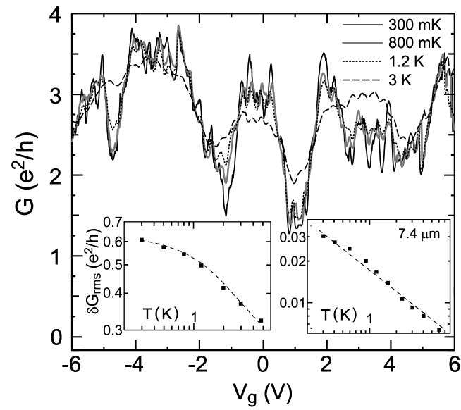
Figure 1 shows the dependence of the conduction of a nm long MWNT device as a function of gate voltage (backgate). Details on device fabrication can be found in Ref. Schoenenberger2 . Large and reproducible fluctuations of order develop in . Note, that the average conductance is quite large, i.e. , and nearly temperature independent. The root-mean square of the conductance fluctuations is displayed in the lower left inset as a function of temperature . For disordered wires random variations of as a function of magnetic field or Fermi energy (which is changed here by the gate) are usually assigned to universal conductance fluctuations (UCF). These fluctuations depend on the specific scattering potential but are universal in the sense that their amplitude at zero temperature is of order , regardless of the sample size and degree of disorder. At finite temperature, self-averaging reduces . For a wire which is D with respect to the phase-coherence length it is given by: , where is the wire length Lee . When becomes of the order of , there is a cross-over to the universal value, Lee . The cross-over appears in the measurement at K and at mK, in good agreement with theory. At this temperature the average conductance amounts to . The saturation of close to the universal limit suggests conduction through one phase coherent unit. This in turns implies that .
As a comparison, we also show of a long MWNT with m in the lower right inset of Fig. 1 For this long nanotube device, , which is reflected in the much smaller amplitude of . at corresponds to nm. This is consistent with the estimate of for the short MWNT and also agrees with deduced from magneto-conductance experiments of other MWNT samples Schoenenberger2 . The dephasing mechanism can be determined from the measured temperature dependence of . Since follows a power-law in over more than one decade with an exponent close to (line in the lower right inset of Fig. 1), . This is the behavior expected for a quasi-D conductor. The main contribution to phase-breaking is caused by electron-electron collisions with small energy transfers, a process known as Nyquist dephasing Altshuler .
In terms of the long NT is a wire, whereas the short one is a dot for which Coulomb blockade (CB) may be important. We now estimate the single-electron charging energy convenience for the latter and compare it with the base measuring temperature K. The dominant contribution to the electrostatic capacitance of short MWNTs is due to the contacts, leading to aF (see below). Hence, K, i.e. , and CB is therefore expected. This, however, does not seem to be the case: firstly, the average conductance is nearly temperature independent (also over a larger temperature range than shown in the graph); secondly, the conductance is large ; and thirdly, lacks the periodicity in gate voltage expected for a weakly coupled quantum dot. We attribute the absence of clear CB features to a large contact transparency. With increasing gate voltage from to V, however, the average conductance decreases from to , possibly reflecting a decreasing contact transparency. This assumption is supported by the following measurement which displays clear Coulomb blockade features in the large gate-voltage regime.
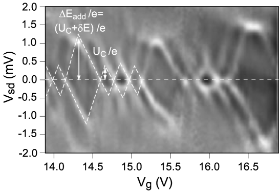
Fig. 2 shows a grey-scale representation of versus gate voltage (horizontal) and transport voltage (vertical) in the regime V. Although the overall two terminal conductance is still large, i.e. , the ‘remainders’ of CB are clearly visible. The most striking observation is a sequence of a large low-conduction CB ‘diamond’ followed by smaller ones (best seen on the left). The diamonds are highlighted by dashed lines in the figure. The size of the CB-diamonds reflects the magnitude of the addition energy , which measures the difference in chemical potential of two adjacent charge states of the dot Kouwenhoven1 . In the constant interaction model (C independent of ) . If all the single-electron levels would repel each other (only 2-fold spin degeneracy) and , an alternating sequence of small and large CB diamonds would be expected. Staring from an even filling number, for the first added electron (large diamond) and to for the second one (small diamond) Nygard . The sequence of one large diamond, followed by three smaller ones of approximate equal size, which is observed here, suggests that the degeneracy of the states is not , but rather (including spin). From the size of the diamonds we obtain meV and meV, the latter corresponding to aF. The total capacitance is the sum of the gate capacitance and the contact capacitances (left) and (right). All three parameters can be deduced from the diamonds. We obtain: aF and aF.
The level spacing of an ideal metallic SWNT is given by , where is the Fermi velocity SpringerReview ; Dresselhaus . This holds for an undoped NT. Recently, it has been found that MWNTs are substantially hole-doped by the environment Krueger . As a consequence more than the ideally expected modes participate in transport. Hence, , where is the number of D subbands. Taking m/s Fermivelocity , the measured value of meV corresponds to , in good agreement with Krüger et al. Krueger . An estimate of the lifetime broadening can be obtained from the measured width of the Coulomb peaks and yields meV.
The observed -fold degeneracy can be explained by a specific property of the graphite sheet (graphene). In the simplest tight-binding band-structure calculation all D-bands are twofold degenerate (not including spin) Dresselhaus . This degeneracy can be traced back to the presence of two C-atoms per unit cell, each contributing with one valence orbital. This, so-called K-K′-degeneracy has not been observed before, although it is supposed to be a generic feature of graphene.
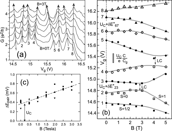
To explore this scenario further we have also studied the gate-voltage shifts of the linear-response conductance peaks as a function of a perpendicular magnetic field , Fig. 3. The difference between the positions of adjacent peaks can also be related to the addition energy: . Figure 3a shows the evolution in small magnetic field T. Adjacent peaks are seen to shift in opposite directions. This is the behavior of a ground-state whose spin alternates as . This, however, contradicts the assumed -fold degeneracy for the following reason: In the presence of a magnetic field the energy of an electron depends on its spin due to the Zeeman effect which lowers the degeneracy from to (only Zeeman energy assumed). For , the two electrons are thus expected to occupy different orbitals with parallel spins. Actually, this would already be expected for , because of exchange-correlation (Hund’s rule would favour the spin-triplet with total angular momentum ) Tarucha . The spin should therefore evolve as for . Experimentally, however, the first electrons have opposite spins and are thus added to the same obital state. This discrepancy can only be resolved, if the assumed -fold degeneracy is not ‘exact’, i.e. there are pairs of states which lie close together with spacing . The pairs themselves are spaced by . A detailed study of the peak evolutions (Fig. 3b) reveals that this is indeed the case. at of the () transition is clearly larger than the and ( and ) ones. We obtain meV and meV, on average meV. We have also verified that the energy shifts agree with the Zeeman term for electrons occupying the same orbital. We plot in Fig. 3c the corresponding addition energies as a function of . A best fit of the data to , where is the Bohr magneton and the Land factor, is shown as a dashed line and yields . This value is consistent with for graphite and with previous measurements of for a SWNT Tans ; Cobden .
In high magnetic field levels cross. Two crossings (LCs) are seen in Fig. 3b. At T, for example, the spin-up of the first orbital crosses the spin-down of the second, giving rise to an transition. A similar crossing is not seen in the upper part. On the one hand, this is due to the larger . On the other hand, there is also a magnetic-field dependence of the orbitals which increases at higher fields.
We find a pattern that repeats every th electron due to an apparent pairing of orbital states. We believe that this pairing is related to the -degeneracy. The splitting is proposed to be caused by hybridization via the contacts, which are strongly coupled to the NT. We expect a level ‘repulsion’, in size comparable to the life-time broadening, which we estimated to be meV. This is in fair agreement with meV. In high magnetic field the intrinsic -degeneracy should be lifted which enhances the level separation further. This may explain why the transition is not observed for the upper quartet in Fig. 3b. Finally, the fact that for at is only consistent with Hund’s rule if the exchange energy , yielding an upper bound for of meV.
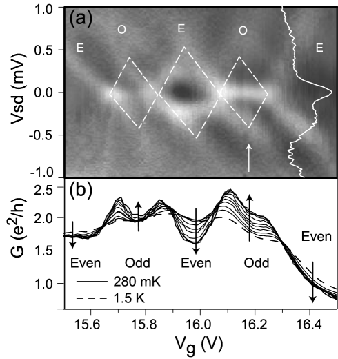
Another interesting manifestation of the electron spin on the electronic transport can be seen in the gate region between and V. We have measured this part with improved accuracy and it is shown in Fig. 4. Fig. 4b shows the linear-response conductance. In the valleys marked as (even filling) the conduction decreases with decreasing temperature while it increases in the valleys marked as (odd filling). Contrary to what one might expect from normal CB, a high conduction ‘ridge’ around V develops in the latter (best seen in the right most diamond). These observations can be understood with the Kondo model Kouwenhoven2 ; Nygard ; Goldhaber . When the number of electrons on the tube is odd and the coupling to the leads is sufficiently strong a spin singlet can form between the spin polarized tube and electrons in the leads. This results in a resonance in the density-of-states at the Fermi energy (i.e. the Kondo resonance). The width of the Kondo resonance reflects the binding energy of the singlet which is usually described by a Kondo temperature . The conductance is expected to increase logarithmically with decreasing temperature in the centers of the ridges below . Following as a function of temperature at V we indeed find a logarithmic dependence between mK and K. At temperatures well below the conductance is expected to saturate at a maximum value of . This is called the unitary limit. In our case, however, no saturation has been observed down to mK.
The Kondo effect is expected to be suppressed by a small bias voltage across the tube of the order of . The ridge at V has a width of 0.2 meV which would correspond to = 1.2 K (see curve in Fig. 4a). This is roughly in agreement with the onset of the logarithmic increase of below 1 K. An additional prediction is the disappearance of the Kondo resonance in a magnetic field. The high conductance ridge indeed broadens and disappears above T. Simultaneously, the Coulomb blockade diamonds are recovered.
We acknowledge W. Belzig, G. Burkard, D. Cobden, R. Egger and J. Nygård for discussions. We thank L. Forró for the MWNT material and J. Gobrecht for providing the oxidized Si substrates. This work has been supported by the Swiss NFS.
References
- (1) For reviews, see: C. Dekker, Physics Today 52 (5), p22-28 (1999); C. Schönenberger and L. Forró, Physics World, June 2001, p37-41.
- (2) S. J. Tans et al, Nature 386,474 (1997).
- (3) M. Bockrath et al. Science 275, 1992 (1997).
- (4) A. Bachtold et al., Phys. Rev. Lett. 84, 6082 (2000).
- (5) L. Forró and C. Schönenberger in Carbon Nanotubes, edited by M.S. Dresselhaus, G. Dresselhaus and Ph. Avouris, Topics in Applied Physics, Vol.80 (Springer 2001).
- (6) L. Langer et al., Phys. Rev. Lett. 76, 479 (1996).
- (7) A. Bachtold et al., Nature 397, 673 (1999).
- (8) C. Schönenberger, A. Bachtold, C. Strunk, J.-P. Salvetat and Forró, Appl. Phys. A 69, 283 (1999).
- (9) L.P. Kouwenhoven et al., in Mesoscopic Electron Transport, edited by L.P. Kouwenhoven, G. Schön, and L.L. Sohn (Kluwer, Dordrecht, The Netherlands, 1997).
- (10) W. Liang et al., Nature 411, 665 (2001).
- (11) J. Nygård, D.H. Cobden, and P. E. Lindelof, Nature 408, 342 (2000).
- (12) P.A. Lee, A.D. Stone, and H. Fukuyama, Phys. Rev. B 35, 1039 (1987); P.A. Lee and A.D. Stone, Phys. Rev. Lett. 55, 1622 (1985).
- (13) B. L. Altshuler, A. G. Aronov, and D. E. Khmelnitsky, J. Phys. C 15, 7367 (1982).
- (14) For convenience we use instead of .
- (15) See e.g., M. S. Dresselhaus, G. Dresselhaus, P. C. Eklund: Science of Fullerenes and Carbon Nanotubes (Academic Press, New York 1996).
- (16) M. Krüger, M. Buitelaar, T. Nussbaumer, and C. Schönenberger, Appl. Phys. Lett. 78,1291 (2001).
- (17) The Fermi velocity of m/s is an upper limit since the average might be lower for a system doped into several subbands.
- (18) S. Tarucha, D.G. Austing, Y. Tokura, W.G. van der Wiel, and L.P. Kouwenhoven, Phys. Rev. Lett. 84, 2485 (2000).
- (19) For a review see: L. Kouwenhoven and L. Glazman in Physics World, January 2001, p.33-38.
- (20) D. Goldhaber-Gorden et al., Nature 391, 156 (1998).
- (21) D. H. Cobden, M. Bockrath, P.L. McEuen, A.G. Rinzler, and R.E. Smalley, Phys. Rev. Lett. 81, 681 (1998).