NON-MAGNETIC SPINGUIDES AND SPIN TRANSPORT IN SEMICONDUCTORS
Abstract
We propose the idea of a ”spinguide”, i.e. the semiconductor channel which is surrounded with walls from the diluted magnetic semiconductor (DMS) with the giant Zeeman splitting which are transparent for electrons with the one spin polarization only. These spinguides may serve as sources of a spin-polarized current in non-magnetic conductors, ultrafast switches of a spin polarization of an electric current and, long distances transmission facilities of a spin polarization (transmission distances can exceed a spin-flip length). The selective transparence of walls leads to new size effects in transport.
1. The interest to the spin transport phenomena constantly grows recently. One of the main problem in this field is creating a spin polarized current in non-magnetic semiconductors (NS). The reason is that combining the magnetic data storage with the electronic readout in one semiconductor device gives a lot of obvious technological advantages. If, in usual ferromagnetic metals we have a spin polarized electric current (in a measure of a difference of a density of states for spin-up and spin-down electrons), than obtaining a stationary spin polarization in NS is fraught with a number of difficulties. The simple idea is to pass a current through the interface ”ferromagnetic metal - semiconductor” [1], but this allows to obtain a negligible current polarization which is smaller than 0.01 % [2]. The reasons of such inefficiency are following. On the one hand, we have the essential conductivity mismatch between the ferromagnetic metal and the semiconductor, and, on the other hand, a spin-flip length is very small in ferromagnetic metals with a good polarizability.
Recently the new extremely effective method of spin polarization of an electric current in NS was realized experimentally [3]. The sample of diluted magnetic semiconductor with a giant splitting of spin subbands in a magnetic field (the effective g-factor about 100) has been used as a spin filter in this experiment (for details of DMS properties see reviews [4], [5]). The idea of the spin filter is based on the following fact. When the Fermi level is under a bottom of one of spin subbands in a DMS a spin-flip scattering is prohibited by virtue of the law of conservation of energy for low enough temperatures. Besides, the DMS has a remarkable affinity with the NS used in the experiment (a semiconductor on the basis of a GaAs), down to coincidens of lattice parameters. Because a spin-flip process in the NS, being a relativistic effect, corresponds to a large mean free path (in some substances up to 100 microns [3], [6]), the system of sequentially connected samples of DMS and NS ideally fits to spin polarization of a current. Accordingly, almost 100 % polarization of the current inflowing from DMS into NS was obtained in the experiment [3].
From an applied point of view, there is an important problem of spins filters application. It is impossible to switch a polarization very fast because of applying high magnetic field. Even for not very high magnetic field the delay time is large in comparison with any mesoscopic time, including the diffusion time. It is also a technological challenge to create a high inhomogeneous field with the change of a sign on microscopic scale. One of the opportunities to obtain fast and compact switches of a spin polarization, overcoming mentioned problems, is to use the ”non-magnetic spinguides” proposed in the present paper.
2. Non-magnetic spinguides. By a ”non-magnetic spinguide” we mean the channel (a wire or a strip) from a NS with walls from a DMS (Fig. 1). Unlike the work [3], in this case the electric current flows along an interface, instead of being normal to it. It is supposed, that spinguide walls let pass electrons with one spin polarization and reflect the another one. In the absence of a current (in an equilibrium situation)the NS channel is unpolarized. However, the current transmitted by a spinguide will be polarized, as nonequilibrium electrons with spins of one of polarization will leave the channel. But for this purpose it is necessary to earth the DMS walls. Otherwise, if spin-flip processes are absent, on an exit from the channel there will be the same unpolarized current, as in the channel entrance.
Let us consider the diffusion transport regime, when the diffusion step is considerably shorter than the channel width : , where is the cyclotron radius, is the electron-impurity mean free path. (We don’t take into account electron-electron collisions, this is a fortiori valid at temperatures about several Kelvin.)
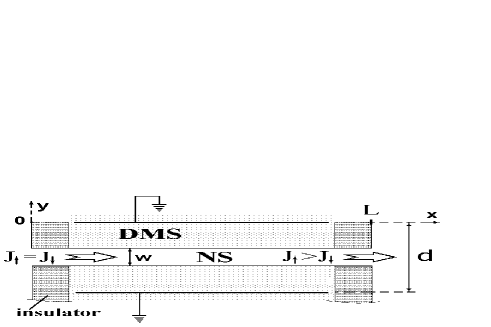
Let be electrochemical potentials of carriers with spins up and down, correspondingly. The densities of electric current are (for simplicity the conductivities in the NS and the DMS are accepted equal). For definiteness sake, let us accept that the walls of the spinguide are transparent for spin-down electrons only, i.e. on the boundaries of the channel (there is supposed to be no dependence on the coordinate ). One should add the earth conditions: on the grounded contacts. Let non-polarized current be input. The diffusion equations can be solved exactly with taking into account these boundary conditions. In the case of , where is the distance between the grounded contacts, at the exit of the channel the current will decrease exponentially with increasing of the channel length: . Taking into account the trivial result , it’s easy to see the spin polarization of a current at the exit from the channel exponentially tends to 1 with increasing of :
| (1) |
It’s natural that spin polarization of current depends essentially on the geometry of grounded contacts.
It’s obvious that the spin polarization in a spinguide is opposite to that appearing in a spin filter scheme [3] at the same direction of DMS polarization. Therefore, combining spin filter and a spinguide with electrostatic gates, it’s easy to switch spin polarization of the current.
Let us note that spin-flip scattering in a NS have a considerably less influence on a current polarization in a spinguide than in a spin filter. In the last case a spin polarization of the current vanishes at the distance where is the mean free path relative to spin-flip processes in a NS. In a spinguide spin-flip processes manifest themselves in essentially different way. They affect the polarization weakly (at ) and lead only to reducing of the total current on the length (for the geometry showed in Fig.1 – according to exponential law).
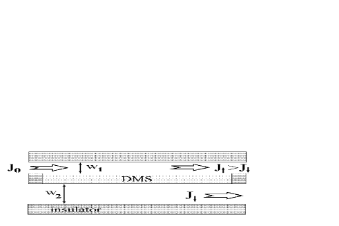
We propose also one more possible design of experiment, namely a ”spin drag” (Fig.2). Non-polarized current is input into channel 1 and this causes entirely polarized current to appear in the channel 2 (which is separated from channel 1 with DMS layer): . But the polarization at the exit of channel 1 will depend on relative width of the channels. In the case of DMS layer thickness being less than the values and at , we have:
| (2) |
The current polarizations in channels 1 and 2 are opposite, but the integral current of two channels, of course, is non-polarized. It’s interesting that for a wide channel 2, , polarized currents will be equally divided between the channels, i.e. in the channel 1 we’ll have entirely polarized current , with equal value and opposite polarization to that in channel 2. It is accepted at the development of formula 2 that the same potential is applied at the exit of channel 2 as at the exit of channel 1. (The latter in our model is determined by the value of current ). Changing the potential at the exit of channel 2,one can control the current polarization in the channels.
3. As one can see from the stated above, spinguides let us achieve a high level of a spin polarization of a current in non-magnetic conductors. Though the use of spin filters also gives a high level of polarization, spinguides can be useful in connection with the opportunity of easy current spin polarization control and long-distance carrying of polarization, in spite of spin-flip scattering. Besides, at the conditions of selective transparency of the boundaries in such systems some interesting features of galvanomagnetic phenomena can appear. In particular, let us note that delocalized states in a magnetic field on the DMS-NS boundaries (corresponding to classic skipping orbits) will be entirely spin-polarized.
References
- [1] P. R. Hammar, B. R. Bennet, M.J. Yang and M.Johnson, Phys.Rev.Lett. 83, 203 (1999).
- [2] G. Shmidt, D. Ferrand, L. A. T. Filip, L. W. Molenkamp and B. J. van Wees, Phys.Rev. B 62, R4790 (2000).
- [3] R. Fiederling, M. Keim, G. Reuscher, W. Ossau, G. Schmidt, A. Waag, L. W. Molenkamp, Nature 402, 787 (1999).
- [4] N. B. Brandt and V. V. Moschchalkov, Adv.Phys. 33, 193 (1984).
- [5] I. I. Liapilin, I. M. Cidilkovsky, UFN 146, 35 (1985).
- [6] V. F. Gantmaher, I. B. Levinson, Current Scattering in Metals and Semiconductors, Nauka, Moscow, 352 p. (1984).