Ab-initio transport theory for digital ferromagnetic heterostructures
Abstract
MnAs/GaAs superlattices, made by -doping GaAs with Mn, are known as digital ferromagnetic heterostructures. Here we present a theoretical density functional study of the electronic, magnetic and transport properties of such heterostructures. In the absence of intrinsic donors these systems show an half metallic density of states, with an exchange interaction much stronger than that of a random alloy with the same Mn concentration. Ab initio ballistic transport calculations show that the carriers with energies close to the Fermi energy are strongly confined within a few monolayers around the MnAs plane. This strong confinement is responsible for the large exchange coupling. Therefore the system can be described as a two dimensional half metal with large conductance in the MnAs plane and small conductance in the perpendicular direction.
pacs:
75.50.Pp, 71.15.Mb, 73.23.Ad, 73.50.-hDiluted magnetic semiconductors (DMS) based on III-V materials Ohno1 ; Ohno2 are receiving great attention for the intriguing interplay between magnetic and electronic properties Ohno3 and for the large potential for future electronic devices Prinz . Ga1-xMnxAs, which is structurally compatible with most epitaxially grown III-V’s, is the prototype of these materials. Here the Mn ions substitute randomly for the Ga ions, providing both localized spins and free carriers (holes). The antiferromagnetic exchange coupling between the hole spin and the Mn spin is responsible for the long range ferromagnetic interaction, which can be described in a first approximation by the Zener model Diet1 . One important result of the model is that the Curie temperature is a linear function of the Mn concentration. Although the inclusion in the model of correlation effects ddsarma modifies this linear dependence, there is general agreement that an increase in the Mn concentration enhances the Curie temperature of the system.
Unfortunately the solubility limit of Mn in GaAs is rather small, since MnAs naturally occurs in a hexagonal phase with [6]-coordinated Mn us1 . However large Mn concentration, up to 50% can be obtained in zincblende MnAs sub-monolayers embedded into GaAs to form a MnAs/GaAs superlattice Rol1 . These structures, called digital ferromagnetic heterostructures (DFH) have remarkable properties. First, the Curie temperature decays for increasing GaAs inter-layer thickness, and saturates for thicknesses larger than 50 GaAs monolayers. The value of at saturation depends on the Mn concentration Rol1 . A saturation is unexpected according to the Zener model for three dimensional systems, since the total Mn concentration in the sample decreases with the increase of the GaAs thickness. This separation dependence suggests that DFH’s behave like planar systems, although to date there is no direct proof that the free carriers responsible for the magnetic interaction are confined in the MnAs layers. Secondly, Hall measurements in the direction parallel to the MnAs planes show an anomalous Hall effect for undoped samples, which disappears upon Be-doping gwin1 ; gwin2 . Large Shubnikov de Haas oscillations are found in doped samples, although surprisingly the charge densities extracted from the Hall coefficient and from the Shubnikov de Haas oscillations are different. This suggests that two different carrier types could be present in the system.
In this letter we investigate theoretically the magnetic and transport properties of undoped DFH. In particular we address the following questions: i) what is the real dimensionality of the system? ii) are the carriers spin-polarized? iii) what is the carrier distribution in the system?
We perform density functional theory kohn calculations in the local spin density approximation. The numerical implementation included in the code siesta siesta uses pseudopotentials and a localized pseudoatomic orbital basis set, and allows us to investigate diluted systems within a supercell approach. Extensive details of the method and its optimization have already been presented us2 . Each DFH superlattice is constructed by considering GaAs cubic cells (8 atoms in the cell) aligned along the direction (see figure 4a). One Ga plane is substituted with Mn and periodic boundary conditions are applied. This leads to an infinite MnAs1/GaAs2N-1 superlattice, where MnAs zincblende monolayers are separated by a Å thick GaAs layer.
In figure 1 we present the band structure for the case (with a 45.2Å thick GaAs inter-layer), for both the majority and minority spins.
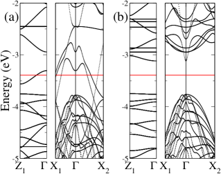
The points and are in the MnAs plane and denote directions along the edge and the diagonal of the cubic supercell respectively. is the direction orthogonal to the MnAs plane. The band structure of figure 1 is that of an half metal, with a gap of approximately 0.65 eV in the minority spin band. The majority spin band presents a strongly anisotropic dispersion. It is metallic and quite dispersive in the MnAs plane (directions ), while in the direction orthogonal to the MnAs plane there is the formation of a narrow impurity band. Since the Fermi energy cuts through the impurity band, MnAs/GaAs looks like a two dimensional half metal with small hopping between the MnAs planes. The width of the impurity band decreases with increasing separation between the MnAs planes (665 meV, 412 meV and 256 meV respectively for =4, =6 and =8), which is consistent with the decrease of the overlap between the wavefunctions centered on the MnAs planes sham .
We calculate the strength of the magnetic coupling by calculating the difference between the total energy of supercells with either antiferromagnetic or ferromagnetic alignment of the Mn ions us3 . We find that the ferromagnetic interaction is much stronger than that in a random alloy with the same Mn concentration. For instance in the MnAs1/GaAs15 DFH with a Mn concentration of =0.06, is 515 meV, whereas in the corresponding random alloy it is only 160 meV. Moreover, seems to be rather independent of the GaAs thickness for the range of thicknesses investigated here (531 meV, 533 meV and 515 meV respectively for =4, =6 and =8), suggesting that the carriers responsible for the ferromagnetism are indeed strongly confined in the MnAs planes.
We also investigate the effect of introducing As antisites (AsGa) by considering a MnAs1/GaAs11 superlattice with half a monolayer of AsGa close to the MnAs plane. This corresponds to one AsGa for two Mn, hence according to the nominal valence, to compensation. In contrast to what expected from the Zener model, the coupling between the Mn ions is still ferromagnetic with =70 meV. This result is similar to that found for the tetrahedral Ga1Mn2As2 complex in GaAs us3 , although in that case =20 meV. We interpret the ferromagnetism at compensation in presence of AsGa as due to localized carriers Zener-coupled to the Mn ions us3 . The MnAs/GaAs superlattices have stronger ferromagnetic coupling than that of the Ga1Mn2As2 complex since the carrier localization close to the MnAs plane is very strong. These results suggest that also in DFH the Curie temperature is determined by a delicate interplay between Mn ions and intrinsic defects.
We now move to the transport properties. Here we generalize the technique of reference us4 to the case of non-orthogonal tight-binding model with singular coupling matrices. The conductance is calculated in the ballistic limit with both the current in the Mn plane (CIP) and perpendicular to the Mn plane (CPP). We first extract the tight-binding Hamiltonian and overlap matrix giving the correct charge density. The matrix elements are computed by numerical integration over a real space grid siesta . The resulting tight-binding Hamiltonian comprises in principle an arbitrary large number of nearest neighbor interactions, which is fixed by the cutoff radius of the pseudoatomic orbitals. We then rewrite both the Hamiltonian and the overlap matrix in a tridiagonal form. This procedure fixes a “natural” length scale. In fact we redefine the unit cell in such a way that each unit cell is coupled only to nearest neighboring cells. Hence the problem is reduced to an effective quasi-one dimensional problem. The scattering matrix is then calculated by a well established Green’s function technique us4 , and the spin conductance by using the Landauer-Büttiker formula but and integrating over the two dimensional Brillouin zone in the plane orthogonal to the direction of transport,
| (1) |
Here spans the two dimensional Brillouin zone in the plane orthogonal to the direction of transport, and is the -dependent transmission matrix for the spin . We assume a two spin fluid model where there is no mixing between majority and minority spins. It is important to point out that in the CPP case our supercell geometry leads to narrow bands. It is then crucial to perform large -point sampling. Here we consider up to 800 -points in the two dimensional irreducible Brillouin zone.

In figure 2 we present the conductance per unit area as a function of the position of the Fermi energy for a MnAs1/GaAs15 superlattice for both the CIP and CPP directions and both spins. We also project the conductance onto the atomic orbital basis set in order to determine the orbital character of the electrons carrying the current us4 . Moreover for the CIP configuration in figure 3 we show the corresponding spin polarization of the conductance , which is defined as .
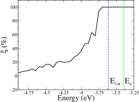
The conductance shows an half metallic behavior for both the CIP and CPP directions. This means that there is a 100% spin polarization of the conductance for undoped samples ( is in the gap for the minority spin). In figure 3 we also show the position of the GaAs valence band edge, which is obtained by aligning the lower lying As levels of bulk GaAs and the MnAs1/GaAs15 superlattice. It is easy to note that is 100% for energies close to the GaAs valence band edge and that the polarization persists well within the valence band. For this reason DFH appear as good candidates for spin injection into -doped GaAs.
If we now analyze closely the conductance of the majority spin band we notice that it is strongly anisotropic, as expected from the bandstructure of figure 1. In the CIP direction the conductance as a function of the position of the Fermi energy is rather flat with an orbital contribution mainly from the As orbital. There is also a significant contribution (roughly 20% of the total conductance) coming from the Mn orbitals, suggesting that the carriers in undoped samples are confined close to the MnAs planes. It is also important to point out that in -space the contributions to the conductance are rather uniformly distributed over the two dimensional Brillouin zone in the plane orthogonal to the transport direction. These are strong indications that MnAs/GaAs is a good isotropic metal in the MnAs planes.
For the CPP direction the situation is rather different. The conductance as a function of the position of shows clear one dimensional features and for undoped samples it is solely given by charge in the impurity band. The orbital content of the impurity band is mainly As with small contributions from Mn . The conductance at comes from few -points around the point. In the case of carriers with parabolic dispersion this happens for scattering at a potential barrier, when the carrier energy is very close to the top of the barrier. In fact carriers with largest kinetic energy in the direction orthogonal to the barrier (small in the parallel direction) have largest transmission amplitude. This situation is similar to that of tunneling junctions and so we describe the transport as tunneling-like.
In summary, from ballistic transport calculations, MnAs/GaAs appears to be a two dimensional half metal in the MnAs plane, with tunneling-like conductance between the MnAs planes. In order to better understand the spatial arrangement of the current in figure 4 we present the charge density distribution in real space, , calculated only for those states contributing to the conductance and within a 0.6 eV range around (). We also notice that the individual contributions from occupied () and unoccupied () states are very similar.
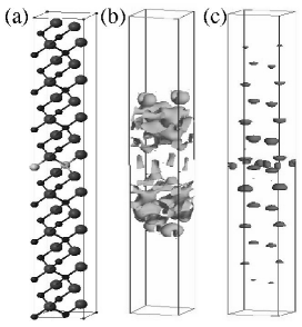
The figure confirms that the current in the CIP case is distributed mainly in a narrow region around the MnAs planes, with small spillage outside. Planar averaging Bald of the charge density of figure 4 shows that the charge density reaches 0.1 of its MnAs plane value within only three GaAs monolayers from the MnAs plane. In contrast, the CPP current is mainly located at the Mn plane with small contributions from the GaAs layers. This means that carriers are strongly confined in the MnAs plane and the perpendicular transport is via hopping between the planes.
Finally in figure 5 we present the macroscopic average Bald of the Hartree potential. The macroscopic average is obtained by first taking a planar average and then by averaging the result over the GaAs lattice spacing. This does not correspond exactly to the total potential which the quasiparticles feel in the structure, but it gives a good indication of the latter Bald .
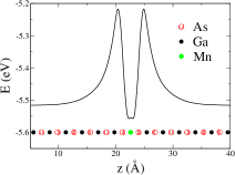
The potential profile shows a deep well in the MnAs plane separated from a flat region by two barriers located one monolayer from the well. The presence of the barrier suggests that -type doping in the GaAs region will only weakly affect the MnAs planes, since the extra electrons need to tunnel through a large barrier to access the MnAs planes.
In conclusion we have studied with ab initio methods the magnetic and transport properties of GaAs/MnAs digital ferromagnetic heterostructures. We have shown that they are two dimensional half metallic systems with large metallic conductance in the MnAs plane, and small tunneling-like conductance perpendicular to the MnAs plane. We have shown that the electronic charge at the Fermi energy is mainly distributed within a few monolayers around the MnAs plane and that the Hartree potential shows a double barrier profile. This potential profile can sustain the presence of a two carrier population for DFH’s that are Be-doped in the GaAs region.
We thank E. Gwinn for stimulating discussions. This work made use of MRL Central Facilities supported by the National Science Foundation under award No. DMR96-32716. This work is supported by ONR grant N00014-00-10557, by NSF-DMR under the grant 9973076 and by ACS PRF under the grant 33851-G5.
References
- (1) H. Ohno, J. Magn. Magn. Mater 200, 110 (1999) and references therein
- (2) H. Ohno, Science 281, 951 (1998)
- (3) H. Ohno, D. Chiba, F. Matsukura, T. Omiya, E. Abe, T. Dietl, Y. Ohno and K. Ohtani, Nature 408, 944 (2000)
- (4) G. Prinz, Science 282, 1660 (1998)
- (5) T. Dietl, H. Ohno, F. Matsukura, J. Cibèrt and D. Ferrand, Science 287, 1019 (2000)
- (6) A. Chattopadhyay, S. Das Sarma and A.J. Millis, cond-mat/0106455
- (7) S. Sanvito, and N.A. Hill, Phys. Rev. B 62, 15553 (2000)
- (8) R.K. Kawakami, E. Johnston-Halperin, L.F. Chen, M. Hanson, N. Guégels, J.S. Speck, A.C. Gossard and D.D. Awschalom, Appl. Phys. Lett. 77, 2379 (2000)
- (9) G. Zanelatto, T. Kreutz, R.K. Kawakami, E. Johnston-Halperin, E. Gwinn, D.D. Awschalom, and A.C. Gossard, Bulletin of the American Physical Society 46, 509 (2001)
- (10) T. Kreutz, G. Zanelatto, R.K. Kawakami, E. Johnston-Halperin, E. Gwinn, D.D. Awschalom, and A.C. Gossard, Bulletin of the American Physical Society 46, 510 (2001)
- (11) H. Hohenberg and W. Kohn, Phys. Rev. 136, B864 (1964), W. Kohn and L. Sham, Phys. Rev. 140 A1133 (1965)
- (12) D. Sánchez-Portal, P. Ordejón, E. Artacho and J.M. Soler, Internat. J. Quantum Chem. 65, 453 (1997) and references therein
- (13) S. Sanvito, P. Ordejón and N.A. Hill, Phys. Rev. B 63, 165206 (2001)
- (14) J. Fernández-Rossier, and L.J Sham, cond-mat/0106548
- (15) S. Sanvito, and N.A. Hill, Appl. Phys. Lett. 78, 3493 (2001)
- (16) S. Sanvito, C.J. Lambert, J.H. Jefferson and A.M. Bratkovsky, Phys. Rev. B 59, 11936 (1999)
- (17) M. Büttiker, Y. Imry, R. Landauer, and S. Pinhas, Phys. Rev. B 31, 6207 (1985)
- (18) S. Baroni, R. Resta, A. Baldereschi, and M. Peressi, in Spectroscopy of Semiconductor Nanostructures, edited by G. Fasol, A. Fasolino and P. Lugli (Plenum, New York, 1989), p.251