Semiconductor Superlattices: A model system for nonlinear transport
Abstract
Electric transport in semiconductor superlattices is dominated by pronounced negative differential conductivity. In this report the standard transport theories for superlattices, i.e. miniband conduction, Wannier-Stark-hopping, and sequential tunneling, are reviewed in detail. Their relation to each other is clarified by a comparison with a quantum transport model based on nonequilibrium Green functions. It is demonstrated how the occurrence of negative differential conductivity causes inhomogeneous electric field distributions, yielding either a characteristic sawtooth shape of the current-voltage characteristic or self-sustained current oscillations. An additional ac-voltage in the THz range is included in the theory as well. The results display absolute negative conductance, photon-assisted tunneling, the possibility of gain, and a negative tunneling capacitance.
keywords:
superlattice transport , nonequilibrium Green functions , THz irradiation , formation of field domainsPACS:
72.20.Ht , 72.10.-d , 73.40.Gk , 73.21.CdNotation and list of symbols
Throughout this work we consider a superlattice, which is grown in the direction. Vectors within the plane parallel to the interfaces are denoted by bold face letters , while vectors in 3 dimensional space are . All sums and integrals extend from to if not stated otherwise.
The following relations are frequently used in this work and are given here for easy reference:
| cross section | |
| spectral function | |
| electron annihilation and creation operators | |
| phonon annihilation and creation operators | |
| period of the superlattice structure | |
| d | integration and differentiation symbol |
| energy | |
| center of energy for miniband | |
| kinetic energy in the direction parallel to the layers | |
| base of natural logarithm | |
| charge of the electron () | |
| electric field in the superlattice direction | |
| semiclassical distribution function | |
| Hamilton operator | |
| imaginary unit | |
| electric current. In section 5 there is an additional prefactor sgn | |
| so that the direction is identical with the electron flow. | |
| current density in the superlattice direction | |
| Bessel function of first kind and order | |
| wavevector in -plane [i.e., plane to superlattice interfaces] | |
| Boltzmann constant | |
| length in superlattice direction | |
| well indices | |
| effective mass of conduction band | |
| electron mass kg. | |
| number of wells | |
| doping density per period and area (unit [cm-2]) | |
| Bose distribution function | |
| Fermi distribution function |
| electron density per period and area (unit [cm-2]) in well | |
| Bloch vector in superlattice direction | |
| coupling between Wannier-states of miniband separated by barriers | |
| temperature | |
| bias applied to the superlattice | |
| argument of Bessel function for irradiation | |
| argument of Bessel functions for Wannier-Stark states | |
| free-particle density of states for the 2D electron gas | |
| density operator | |
| one-particle density matrix | |
| indices of energy bands/levels | |
| chemical potential in well , measured with respect to the bottom of the well | |
| frequency of the radiation field | |
| electrical potential | |
| Bloch function of band | |
| Wannier function of band localized in well | |
| Wannier-Stark function of band centered around well | |
| scattering time | |
| Heavyside function for and for | |
| imaginary part | |
| real part | |
| principal value | |
| order of | |
| commutator | |
| anticommutator |
1 Introduction
In this review, the transport properties of semiconductor superlattices are studied. These nanostructures consist of two different semiconductor materials (exhibiting similar lattice constants, e.g., GaAs and AlAs), which are deposited alternately on each other to form a periodic structure in the growth direction. The technical development of growth techniques allows one to control the thicknesses of these layers with a high precision, so that the interfaces are well defined within one atomic monolayer. In this way it is possible to tailor artificial periodic structures which show similar features to conventional crystals.
Crystal structures exhibit a periodic arrangement of the atoms with a lattice period . This has strong implications for the energy spectrum of the electronic states: Energy bands [1] appear instead of discrete levels, which are characteristic for atoms and molecules. The corresponding extended states are called Bloch states and are characterized by the band index and the Bloch vector . Their energy is given by the dispersion relation . If an electric field is applied, the Bloch states are no longer eigenstates of the Hamiltonian, but the Bloch vector becomes time dependent according to the acceleration theorem
| (1) |
where is the charge of the electron. Since the Bloch vectors are restricted to the Brillouin zone, which has a size , a special feature arises when the acceleration of the state lasts for a time of : If interband transitions are neglected, the initial state is then reached again, and the electron performs a periodic motion both in the Brillouin zone and in real space [2], which is conventionally referred to as a Bloch oscillation. For typical materials and electric fields, is much larger than the scattering time, and thus this surprising effect has not been observed yet in standard crystals.
In 1970, Esaki and Tsu suggested that superlattice structures with an artificial period can be realized by the periodically repeated deposition of alternate layers from different materials [3]. This leads to spatial variations in the conduction and valence band of the material with period implying the formation of energy bands as sketched in Fig. 1.
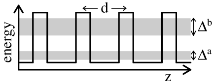
Both the energy width of these bands, as well as the extension of the Brillouin zone, are much smaller than the corresponding values for conventional conduction bands. Thus, the energy bands originating from the superlattice structure are called minibands. As can be significantly larger than the period of the crystal, can become smaller than the scattering time for available structures and applicable electric fields.
It is crucial to note that the picture of Bloch-oscillations is not the only possibility to understand the behavior of semiconductor superlattices in an electric field. The combination of a constant electric field and a periodic structure causes the formation of a Wannier-Stark ladder [4], a periodic sequence of energy levels separated by in energy space. This concept is complementary to the Bloch-oscillation picture, where the frequency corresponds to the energy difference between the Wannier-Stark levels.
Both the occurrence of Bloch oscillations and the nature of the Wannier-Stark states predict an increasing localization of the electrons with increasing electric field. This causes a significant drop of the conductivity at moderate fields, associated with the occurrence of negative differential conductivity [3]. Similar to the Gunn diode, this effect is likely to cause the formation of inhomogeneous field distributions. These provide various kinds of interesting nonlinear behavior, but make it difficult to observe the Bloch oscillations.
The presence of a strong alternating electric field (with frequency in the THz range) along the superlattice structure provides further interesting features. Both photon-assisted resonances (shifted by from the original resonance) and negative dynamical conductance have been predicted on the basis of a simple analysis [5]. For specific ratios between the field strength and its frequency, dynamical localization [6] occurs, i.e. the dc-conductance becomes zero, which can be attributed to the collapse of the miniband [7].
Some fundamental aspects of superlattice physics have already been reviewed in Ref. [8]. Refs. [9, 10] consider the electronic structure in detail and the review article [11] focuses on infrared spectroscopy. Much information regarding the growth processes as well as transport measurements can be found in Ref. [12]. The relation between Bloch oscillations and Wannier-Stark states has been analyzed in [13]. Ref. [14] provides an early review on high-frequency phenomena. In addition to superlattices consisting of different semiconductor materials, it is possible to achieve similar properties by a periodic sequence of n- and p-type doped layers [15].
1.1 Experimental summary
A large variety of superlattice structures has been studied since the original proposal of Esaki and Tsu in 1970. These investigations can be divided into four different areas: the nonlinear current-field relation and its implications, the Wannier-Stark ladder, the search for Bloch oscillations, and the interaction with THz-fields.
The simple model by Esaki and Tsu [3] predicts a nonlinear current-field relation exhibiting a maximum for field strengths of , where denotes the scattering time. For higher fields, the current drops with increasing field, yielding a region of negative differential conductivity. Such behavior was first observed in the experiment by Esaki and Chang [16] in 1974, where the conductance exhibited a sequence of dips, reaching negative values, as a function of bias voltage. This complicated behavior was attributed to the formation of domains with two different field values in the superlattice. With improving sample quality the sawtooth structure of the current-voltage characteristic due to domain formation could be resolved [17] more than a decade later. Traveling field domains (already proposed in 1977 [18]) were observed as well [19]. They cause self-generated current oscillations with frequencies up to 150 GHz [20]. Domain formation effects typically hinder the direct observation of negative differential conductance, as there is no simple proportionality between the measured bias and local electric field in the sample. In Ref. [21], the local relation between current and field could be extracted from an analysis of the global current-voltage characteristic. A direct observation of the Esaki-Tsu shape was possible from time-of-flight-measurements [22], and the analysis of the frequency response [23].
The concept of the Wannier-Stark ladder could be corroborated by the observation of the typical spacing in the optical excitation spectrum of superlattice structures [24, 25]. More recent studies refer to the transition between the Franz-Keldysh oscillations and the Wannier-Stark ladder [26], and the influence of higher valleys in the band structure [27].
The dynamical nature of Bloch oscillations with period was observed by transient four-wave mixing [28] and by a direct observation of the THz emission at [29]. Under stationary conditions, the phases for the oscillation cycles of individual electrons are randomized by scattering processes, and the global signal averages out. Therefore, decaying signals have been observed in these experiments after a short pulse excitation, which synchronizes the dynamics in the very beginning. More recently, the spatial extension of the Bloch-oscillation was resolved by measuring its dipole field [30].
With the development of strong THz sources, the interaction of THz fields with transport through superlattices have been studied in the last few years. In particular, dynamical localization, photon-assisted tunneling, and absolute negative conductance were observed under irradiation by a free-electron laser [31]. Recent work aims at applying these effects to the detection of THz signals [32].
Further experiments will be discussed in the subsequent sections in direct comparison with the theory.
1.2 Outline of this work
In this work the theory of electrical transport in semiconductor superlattices is reviewed with a strong emphasis towards nonlinear electric transport. Here two different issues arise, which will be treated thoroughly:
How can the electric transport in semiconductor structures be described quantitatively? This is not a straightforward issue as different energy scales like the miniband width, the scattering induced broadening, and the potential drop per period are typically of the same order of magnitude in semiconductor superlattices. For this reason, standard concepts from bulk transport (like the semiclassical Boltzmann equation), which rely on the large band width, become questionable. Therefore, different approaches, such as miniband transport [3], Wannier-Stark hopping [33], or sequential tunneling [34, 35], have been suggested to study the transport properties of semiconductor superlattices. These standard approaches imply different approximations, and their relation to each other was only recently resolved within a quantum transport theory [36]. As a result, one finds that all standard approaches are likely to fail if the miniband width, the scattering induced broadening, and the potential drop per period take similar values. In this case, one has to apply a full quantum transport calculation. For the linear response, the quantum aspects of the problem can be treated within the Kubo formula [37], which is evaluated in thermal equilibrium. For the nonlinear transport discussed here, this is not sufficient and a more involved treatment of nonequilibrium quantum transport is necessary. An overview regarding different aspects of quantum transport in mesoscopic systems can be found in recent textbooks [38, 39, 40, 41, 42].
What is the implication of a strongly nonlinear relation between the current-density and the local field? As long as the field and current distribution remain (approximately) homogeneous, the ratio between this local relation and the global current-voltage characteristic is given by geometrical factors. In the region of negative differential conductivity, the stationary homogeneous field distribution becomes unstable, which may lead to complex spatio-temporal behavior. Typically, one observes complex scenarios, where current filaments or electric field domains form, which may yield both stationary or oscillating behavior. In some cases, chaotic behavior is observed as well. Such effects can be treated within standard concepts of nonlinear dynamics for a variety of different semiconductor systems [43, 44, 45, 46, 47].
The nature of quantum transport as well as pronounced nonlinearities are characteristic problems of high-field transport in semiconductor nanostructures. In such structures the electric transport is determined by various quantum phenomena such as resonant tunneling (e.g. the resonant tunneling diode [48]), or transmission through funnel injectors (e.g. in the quantum cascade laser [49]). In such cases, neither standard semiclassical bulk transport models nor linear-response theories apply, and more advanced simulation techniques are required. The excellent possibilities for tailoring different structures with specific superlattice periods, miniband widths, or doping densities make semiconductor superlattices an ideal testing ground for nonlinear quantum transport.
This review is organized as follows: Section 2 introduces the basis state functions, such as Bloch, Wannier, or Wannier-Stark states, which will be used in the subsequent sections. In particular, it is shown how the miniband widths and coupling parameters can be calculated from the material parameters on the basis of the envelope function theory. Section 3 reviews the three standard approaches of superlattice transport: miniband transport, Wannier-Stark hopping, and sequential tunneling. Each of these approaches is valid in a certain parameter range and allows for a quantitative determination of the current density. It is a common feature of these approaches that they display negative differential conductivity in qualitative agreement with the simple Esaki-Tsu result. These approaches can be viewed as limiting cases of a quantum transport theory, which is derived in section 4 on the basis of nonequilibrium Green functions. The occurrence of stationary and traveling field domains in long superlattices structures is discussed in section 5. Here, specific criteria are presented, which allow the prediction of the global behavior on the basis of the current-field relation and the contact conditions. Finally, transport under irradiation by a THz field is addressed in section 6. Some technical matters are presented in the appendices.
2 States in superlattices
In order to perform any quantum calculation one has to define a basis set of states to be used. While in principle the exact result of any calculation must not depend on the choice of basis states, this does not hold if approximations are made, which is necessary for almost any realistic problem. Now different sets of basis states suggest different kinds of approximations and therefore a good choice of basis states is a crucial question. For practical purposes the basis set is usually chosen as the set of eigenstates of a soluble part of the total Hamiltonian. If the remaining part is small, it can be treated in lowest order of perturbation theory (e.g., Fermi’s golden rule for transition rates) which allows for a significant simplification. This provides an indication for the practicability of a set of states.
In the following discussion we restrict ourselves to the states arising from the conduction band of the superlattice, which is assumed to be a single band with spin degeneracy. All wave functions employed in the following have to be considered as envelope functions with respect to this conduction band, which are determined by the Schrödinger-like equation
| (2) |
where denotes the effective mass in the conduction band. Assuming ideal interfaces, the structure is translational invariant within the and direction perpendicular to the growth direction. Therefore the dependence can be taken in the form of plane waves where and are vectors within the two-dimensional plane. The crucial point in this section is the choice of the dependence of the basis states. This reflects the current direction considered here and has therefore strong implications on the description of transport.
Semiconductor superlattices are designed as periodic structures with period in the growth direction. Thus their eigenstates can be chosen as Bloch-states (where denotes the Bloch-vector and is the band index) which extend over the whole structure. The corresponding eigenvalues of the Hamiltonian form the miniband (subsection 2.1). This provides the exact solution for a perfect superlattice without applied electric field. An alternative set of basis functions can be constructed by employing localized wave functions which resemble eigenstates of single quantum wells labeled by the index . Here we use the Wannier-states , which can be constructed separately for each miniband (subsection 2.3). At third we may consider the Hamiltonian of the superlattice in the presence of a finite electric field . Then the energy levels take the form and one obtains the Wannier-Stark states , where we neglect the field-dependent coupling between the subbands (subsection 2.4). The spatial extension of these states is inversely proportional to the electric field. In the subsequent subsections the different basis sets will be derived and their properties will be studied in detail.
2.1 Minibands
The periodicity of the superlattice structure within the direction implies that the eigenstates of the Hamiltonian can be written as Bloch states , where denotes the Bloch vector. The construction of these eigenstates can be performed straightforward within the transfer matrix formulation, see e.g. [50, 51]. Within a region of constant potential and constant material composition the envelope function can be written as . Then the connection rules [52] (see also Refs. [10, 51, 53] for a detailed discussion)
| (3) | |||||
| (4) |
apply111Throughout this work we use the energy dispersion with the band edge meV and the effective mass for the conduction band of AlxGa1-xAs with [54]. For GaAs/AlAs structures, nonparabolicity effects are included using the energy-dependent effective mass with the parameters , , meV for GaAs and , meV, meV for AlAs [55, 56], where denotes the edge of the valence band. X,L-related effects are neglected for simplicity. They become relevant in some transport studies [57]. Some approaches to the theoretical study of tunneling via these minima can be found in [58, 59, 60].where is the effective mass in region .
| (5) |
with
| (6) |
If a single period of the superlattice consists of regions with constant material composition, the Bloch-condition implies
| (7) |
For standard superlattices () the solutions resemble those of the Kronig-Penney model [61], except for the use of effective masses associated with the connection rule (4). Within the transfer formalism the extension to superlattices with a basis [62] (larger ) is straightforward. For given , Eq. (7) is only solvable for selected values of which define the miniband-structure . An example is shown in Fig. 2. Next to the envelope function approximation discussed here, different approaches can be used to calculate the superlattice band structure [9, 63].

For a given miniband the following quantities may be defined:
| center of miniband: | (8) | ||||
| miniband width: | (9) |
which characterize the miniband structure. For the miniband structure shown in Fig. 2 the values meV, meV, meV, meV, meV, and meV are found, where the band indices are labeled by . The increase of with can be easily understood in terms of the increasing transparency of the barrier with the electron energy. As is restricted to and by Kramers degeneracy, the function can be expanded as follows:
| (10) |
Typically, the terms for are much smaller than the term. E.g., for the bandstructure of Fig. 2 one obtains meV, meV for the lowest band, meV, meV for the second band, and meV, meV for the third band. This demonstrates that the band structure is essentially of cosine-shape and thus . The dispersion can be viewed as the result of a standard tight-binding calculation with next-neighbor coupling .
In order to perform many-particle calculations the formalism of second quantization, see, e.g., [65], is appropriate. Let and be the creation and annihilation operator for electrons in the Bloch-state of band with Bloch-vector . Then the Hamiltonian reads
| (11) |
which is diagonal in the Bloch-states, as the Bloch-states are eigenstates of the unperturbed superlattice.
2.2 Bloch-states of the three-dimensional superlattice
In the preceding subsection only the direction of the superlattice was taken into account. For an ideal superlattice Eq. (2) does not exhibit an -dependence and thus a complete set of eigenstates states can be constructed by products of plane waves and a -dependent function which satisfies the eigenvalue equation
| (12) |
As and are periodic functions with the superlattice period , the eigenstates are Bloch state with energy .222Eq. (12) shows that the effective Hamiltonian is not exactly separable in a and r-dependent part, as the -dependent effective mass affects the k-dependence, describing the behavior in the plane. Nevertheless, this subtlety is not taken into account here, as discussed below. Within first order perturbation theory in one obtains the energy
| (13) |
Now will exhibit a larger probability in the well, so that it seems reasonable to replace the second term by
| (14) |
where is the effective mass of the quantum well. In analogy to Eq. (11) the full Hamiltonian reads
| (15) |
where and are the creation and annihilation operator for electrons in the Bloch-state of band with Bloch-vector and wave vector in plane. In order to evaluate matrix elements for scattering processes the zeroth order envelope wave-functions are applied in subsequent sections. The treatment is completely analogous for Wannier and Wannier-Stark states discussed in the subsequent subsections.
2.3 Wannier functions
By definition the Bloch-functions are delocalized over the whole superlattice structure. This may provide difficulties if electric fields are applied or effects due to the finite length of the superlattice are considered. Therefore it is often helpful to use different sets of basis states which are better localized. A tempting choice would be the use of eigenstates of single quantum wells, see, e.g., [66, 67]. Nevertheless such a choice has a severe shortcoming: The corresponding states are solutions of two different Hamiltonians, each neglecting the presence of the other well. Thus these states are not orthogonal which provides complications. Typically, the coupling is estimated by the transfer Hamiltonian [68] within this approach.
For these reasons it is more convenient to use the set of Wannier functions [69]
| (16) |
which are constructed from the Bloch functions with the normalization . Here some care has to be taken: The Bloch functions are only defined up to a complex phase which can be chosen arbitrarily for each value . The functions depend strongly on the choice of these phases. In [70] it has been shown that the Wannier functions are maximally localized if the phase is chosen in the following way at a symmetry point of the superlattice: If choose (i). Otherwise choose (ii). In both cases the phase is chosen such, that is an analytic function in . (The latter requirement defines the phase when becomes zero and prevents from arbitrary sign changes of .) For such a choice the Wannier functions are real and symmetric (i) or antisymmetric (ii) around . Now there are two symmetry points, one in the center of the well () and one in the barrier (), for a typical superlattice. If the energy of the miniband is below the conduction band of the barrier, the Wannier functions seem to be strongly localized for , while may be suited as well for larger energies, where the minibands are above the barrier. This point has also been addressed in [71]. In Fig. 3 the Wannier functions for the first two bands (using ) are displayed.

One finds that both functions are essentially localized to the central quantum well where they resemble the bound states. Outside the well they exhibit a decaying oscillatory behavior which ensures the orthonormality relation333Note that the orthonormality is not strictly fulfilled for different bands if an energy dependent effective mass is used. In this case, energy-dependent Hamiltonians (2) are used for the envelope functions, and therefore the orthonormality of eigenfunctions belonging to different energies is not guaranteed. In principle this problem could be cured by reconstructing the full wave functions from the envelope functions under consideration of the admixtures from different bands.
| (17) |
Within second quantization the creation and annihilation operators of the states associated with the Wannier functions are defined via
| (18) |
Inserting into Eq. (11) and using Eq. (10) one obtains the Hamiltonian within the Wannier basis
| (19) |
As the Wannier functions are linear combinations of Bloch functions with different energies, they do not represent stationary states. Neglecting terms with the time evolution of the annihilation operators in the Heisenberg representation is given by
| (20) |
For the initial condition this set of equations has the solution
| (21) |
where is the Bessel function of first kind [72]. This shows that the initially occupied Wannier state decays on a time scale of
| (22) |
At this time , thus may be viewed as a kind of half-life period, although there is no exponential decay.
If an electric field is applied to the superlattice, the additional potential has to be taken into account. Within the Wannier basis the corresponding terms of the Hamiltonian can be evaluated directly by the corresponding matrix elements . Including the parallel degrees of freedom , the total Hamiltonian reads:
| (23) | |||||
| (24) | |||||
| (25) |
with the couplings . If the superlattice exhibits inversion symmetry the coefficients vanish for . Finally note, that the expression of is still exact, except for the separation of and direction.
The term describes the energy of the states in the superlattice neglecting any couplings to different bands or different wells. gives the coupling between different wells. Finally describes the field-dependent mixing of the levels inside a given well. In particular it is responsible for the Stark shift.
The term for can be diagonalized [73] by constructing the new basis
| (26) |
satisfying where the columns of are the components of with respect to the basis . This shows, that the level separation becomes field dependent, which has been recently observed in superlattice transport [74] under irradiation. In the new basis the Hamiltonian is given by with
| (27) | |||||
| (28) |
and the matrix elements
| (29) |
It will turn out later that in the limit of sequential tunneling it is more appropriate to use as a perturbation instead of .
2.4 Wannier-Stark ladder
If an electric field is applied to the superlattice structure the Hamiltonian exhibits an additional scalar potential which destroys the translational invariance. In this case we can easily see: If there exists an eigenstate with wavefunction and energy , then the set of states corresponding to wavefunctions are eigenstates of the Hamiltonian with energies as well. These states are equally spaced both in energy and real space and form the so-called Wannier-Stark ladder [4]. This feature has to be considered with some care, as the potential is not bounded for the infinite crystal, which implies a continuous energy spectrum [75]. Nevertheless, the characteristic energy spectrum of these Wannier-Stark ladders could be resolved experimentally [24, 25] in semiconductor superlattices. For a more detailed discussion of this subject see [13, 76, 77].
If one restricts the Hamiltonian in Eq. (11) to a given miniband , an analytical solution for the eigenstates of exists [78]:
| (30) |
where is the ladder of energies corresponding to the miniband with average energy similar to the discussion of the Wannier states444This representation depends crucially on the relative choice of phases in the Bloch functions . The situation resembles the construction of Wannier states (16) and it is suggestive to use the same choice of phase although I am not aware of a proof. For consistency the origin of has to be chosen such that holds for the symmetry point of the superlattice.. The field-induced coupling to different bands induces a finite lifetime of these single band Wannier-Stark states due to Zener tunneling [78]. Thus these Wannier-Stark states can be viewed as resonant states (an explicit calculation of these resonances has been performed in [79]). For a cosine-shaped band the Wannier-Stark states from Eq. (30) can be expanded in Wannier states [80]
| (31) |
where the definition (16) has been used. This relation can be obtained directly by diagonalizing Eqs. (23,24) within the restriction to a single band, nearest-neighbor coupling , and , i.e. . In Fig. 4 examples for the Wannier-Stark states are shown.

It can be clearly seen that the localization of these states increases with the electric field. They exhibit an oscillatory structure within a region of approximately periods and a strong decay outside this region. This magnitude can be estimated via Eq. (31). As [Eq. (8.536(2) of [81]] we can conclude that deviates from zero essentially in the range which, together with , provides the result given above.
3 The standard approaches for superlattice transport
If an external bias is applied to a conductor, such as a metal or a semiconductor, typically an electrical current is generated. The magnitude of this current is determined by the band structure of the material, scattering processes, the applied field strength, as well as the equilibrium carrier distribution of the conductor. In this section the question is addressed, how the special design of a semiconductor superlattice, which allows to vary the band-structure in a wide range, influences the transport behavior. Throughout this section we assume that a homogeneous electrical field is applied in the direction of the superlattice (the direction) and consider the current parallel to this field. Due to symmetry reasons the transverse current parallel to the layers should vanish.
A very elementary solution to the problem has been provided by Esaki and Tsu in their pioneering paper [3]. Consider the lowest miniband of the superlattice labeled by the superscript . The eigenstates are the Bloch-states with the Bloch-vector and the dispersion is approximately given by (see Sec. 2.1 for details) as depicted in Fig. 5a. At low temperatures the states close to the minimum at are occupied in thermal equilibrium. If an electric field is applied (in -direction) the Bloch-states are no longer eigenstates of the full Hamiltonian but change in time. According to the acceleration theorem [1]
| (32) |
the states remain Bloch states in time, but the Bloch-vector becomes time dependent and we find if the electron starts in the minimum of the band at . For the boundary of the Brillouin zone () is reached. This point is equivalent with the point at , so that the trajectory continues there which is often called Bragg-reflection. Finally, at the origin is reached again. Neglecting transitions to different bands (Zener transitions, whose probability is extremely small for low fields) the state remains in the given band and thus the same state is reached after resulting in a periodical motion of the state through the Brillouin zone [2]. This oscillation is called Bloch-oscillation and is quite general for arbitrary bandstructures. It could be observed in superlattices [28, 29]. The Bloch-states travel with the velocity
| (33) |
Thus, we find and the position of a wave packet with and . In [82] this behavior has been nicely demonstrated by an explicit solution of the Schrödinger equation. The spatial amplitude of this oscillation has been resolved recently [30].

Scattering processes will interrupt this oscillatory behavior. As scattering processes are likely to restore thermal equilibrium it makes sense to assume that the scattered electron will be found close to , the initial point used before. As long as the average scattering time is much smaller than the electrons will remain in the range where the velocity increases with and thus an increase of will generate larger average drift velocities. Thus for a linear increase of is expected. In contrast, if the electrons reach the region with negative velocities and thus the average drift velocity can be expected to drop with the field for . For high fields, , the electrons perform many periods of the Bloch-oscillation before they are scattered and thus the average drift velocity tends to zero for . A detailed analysis for a constant (momentum-independent) scattering time gives the Esaki-Tsu relation [3]:
| (34) |
This result will be derived in Sec. 3.1.1 as well. The drift velocity exhibits a linear increase with for low fields, a maximum at and negative differential conductivity for , see Fig. 5b. This general behavior could be observed experimentally [83, 22].
The rather simple argument given above neglects the plane wave states in -direction, the thermal distribution of carriers, and treats scattering processes in an extremely simplified manner. In Section 3.1 a more realistic treatment is given within the miniband transport model where the electrons occupy Bloch-states and the dynamical evolution of the single states is described by the acceleration theorem (32).
A complementary approach to miniband transport is the use of Wannier-Stark states, which are the ’real’ eigenstates of the superlattice in an electric field [see Sec. 2.4 for a discussion of the problems involved with these states]. Scattering processes cause transitions between these states yielding a net current in the direction of the electric field [33]. This approach is called Wannier-Stark hopping and will be described in detail in Sec. 3.2.
For superlattices with thick barriers (i.e. narrow minibands) it seems more appropriate to view the structure as a series of weakly-coupled quantum wells with localized eigenstates. Due to the residual coupling between the wells tunneling processes through the barriers are possible and the electrical transport results from sequential tunneling from well to well, which will be discussed in Sec. 3.3. Generally, the lowest states in adjacent wells are energetically aligned for zero potential drop. Thus, the energy conservation in Fermi’s golden rule would forbid tunneling transitions for finite fields. Here it is essential to include the scattering induced broadening of the states which allows for such transitions.
| coupling | voltage drop | scattering | |
|---|---|---|---|
Miniband conduction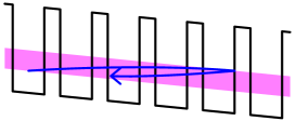
|
exact: miniband | acceleration | golden rule |
Wannier-Stark hopping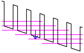
|
exact: Wannier Stark states | golden rule | |
Sequential tunneling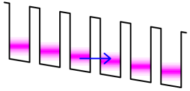
|
lowest order | energy mismatch | ”exact” spectral function |
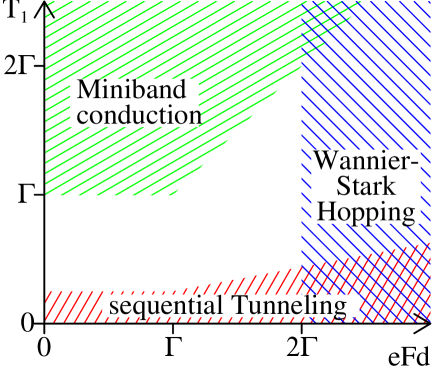
These three complementary approaches are schematically depicted in Fig. 6. They treat the basic ingredients to transport, band structure (coupling ), field strength (), and scattering (), in completely different ways. In section 4 and appendix B these approaches will be compared with a quantum transport model, which will determine their respective range of validity as sketched in Fig. 7.
It is an intriguing feature that all three approaches provide a velocity-field relation in qualitative agreement with Fig. 5b, except that the linear increase is missing in the Wannier-Stark hopping model. Therefore the qualitative features from the Esaki-Tsu model persist but details as well as the magnitude of the current may be strongly altered. These points will be discussed in detail in the subsequent subsections.
3.1 Miniband transport
Conventionally, the electrical transport in semiconductors or metals is described within a semiclassical approach. Due to the periodicity of the crystal, a basis of eigenstates from Bloch-functions can be constructed. For the superlattice structure considered here it is convenient to treat the Bloch-vector in superlattice direction and the Bloch-vector in the direction parallel to the layers separately. The eigenfunctions are and the corresponding energies are with the superlattice dispersion and the in-plane energy , for details see Sec. 2.1. The occupation of these states is given by the distribution function describing the probability that the state is occupied and is the particle density within the the volume element in momentum space.
An electric field breaks the translational invariance of the system and the Bloch states are no longer eigenstates. Within the semiclassical theory the temporal evolution of the distribution function is given by the Boltzmann equation555If spatially inhomogeneous distributions are considered, the convection term has to be added on the left hand side.
| (35) |
which is derived in most textbooks on solid state physics. (The inclusion of magnetic fields is straightforward and results for superlattice structures are given in [84, 85]; see also [86] for corresponding experimental results. Recently, a mechanism for spontaneous current generation due to the presence of hot electron in a magnetic field perpendicular to the superlattice direction was proposed [87].) The right side describes the change of the distribution function due to scattering. For impurity or phonon scattering the scattering term reads
| (36) |
denotes the scattering probability from state to state which can be calculated by Fermi’s golden rule using appropriate matrix elements for the different scattering processes. Details regarding these scattering processes (for bulk systems) can be found textbooks, such as [88, 89]. Specific calculations for superlattice structures can be found in [90, 91, 92]. Once the distribution function is known, the current density for miniband transport in direction can be evaluated directly by
| (37) |
and the electron density per superlattice period (in units [1/cm2]) is given by
| (38) |
This approach for the electric transport is called miniband transport. An earlier review has been given in [93] where several experimental details are provided.
One has to be aware that Boltzmann’s equation holds for classical particles under the assumption of independent scattering events. The only quantum mechanical ingredient is the use of the dispersion , thus the term semiclassical approach is often used. Therefore deviations may result from various quantum features, such as scattering induced broadening of the states, the intracollisional field effect, or correlations between scattering effects leading, e.g., to weak localization. While these features are notoriously difficult to describe, operational solution methods like Monte-Carlo methods [94, 95] exist for the Boltzmann equation explaining the popularity of the semiclassical approach.
3.1.1 Relaxation time approximation
Boltzmann’s equation can be solved easily if the scattering term is approximated by
| (39) |
with the relaxation time . The relaxation time approximation is correct in the linear response regime for a variety of scattering processes. Here it is applied to nonlinear transport, in order to obtain some insight into the general features. The underlying assumption is that any scattering process restores the thermal equilibrium described by the Fermi function and the chemical potential . (The discussion is restricted to the lowest miniband here and thus the miniband index is neglected.) Then the stationary Boltzmann equation reads:
| (40) |
This is an inhomogeneous linear partial differential equation which, together with the boundary condition , can be integrated directly and one finds:
| (41) |
Assuming a constant scattering rate , the integrals become trivial. For the simplified miniband structure one obtains the electron density from Eq. (38)
| (42) |
and the current density from Eq. (37)
| (43) |
with
| (44) |
Note that the field dependence of the current density is identical with the simple Esaki-Tsu result (34), but the prefactor has a complicated form, which will be analyzed in the following. The -integration can be performed analytically in and .
| (45) |
Here is the density of states of the two-dimensional electron gas parallel to the layers including spin degeneracy.
At first consider the degenerate case which holds for low temperatures . If one obtains [96] and
| (46) |
This expression is independent from the carrier density. (For superlattices with very thin barriers a different behavior has been reported [97] which was explained by the one-dimensional character of the tranport due to inhomogeneities.) A second instructive result is obtained for very low densities when
| (47) |
holds and thus
| (48) |
which gives providing the Esaki-Tsu result (34) mentioned above.
In the non-degenerate case one obtains [8]
| (49) | |||||
| (50) |
with the modified Bessel functions , see Eq. (9.6.19) of [72]. For low temperatures the argument of the Bessel functions becomes large and . Then Eq. (48) is recovered again. For high temperatures the Bessel functions behave as and , and
| (51) |
Such a dependence of the current density has been observed experimentally in [98, 99] albeit the superlattices considered there exhibit a rather small miniband width and the justification of the miniband transport approach is not straightforward.
3.1.2 Two scattering times
A severe problem of the relaxation-time model is the fact that all scattering processes restore thermal equilibrium. While this may be correct for phonon scattering, where energy can be transferred to the phonon systems, this assumption is clearly wrong for impurity scattering, which does not change the energy of the particle. The significance of this distinction can be studied by applying the following scattering term [5, 100]
| (52) |
Here scattering processes which change both momentum and energy are contained in the energy scattering time and elastic scattering events, changing only the momentum, are taken into account by . While the Boltzmann equation was solved explicitly in Sec. 3.1.1, dynamical equations for the physical quantities of interest are derived here by taking the appropriate averages with the distribution function. At first consider the electron density (38). Performing the integral of Eq. (35) one obtains
| (53) |
where the periodicity of has been used to eliminate the term . Therefore the electron density is again given by , see Eq. (42). In the same manner one obtains (using integration by parts in the term )
| (54) |
with the momentum relaxation time and the average
| (55) |
Finally, the dynamical evolution of is given by
| (56) |
This equation can be considered as a balance equation for the kinetic energy in the superlattice direction as . The stationary solution of Eqs. (54,56) gives
| (57) |
with the effective scattering time and . This is just the result (43) with the additional factor reducing the magnitude of the current, as . The prefactors and are identical with those introduced in the last subsection.
The relaxation time approximation has proven to be useful for the analysis of experimental data by fitting the phenomenological scattering times . In [101] the times s and s has been obtained for a variety of highly-doped and strongly-coupled superlattices at K.
It should be noted that there is an instructive interpretation [102] of Eq. (57) which may be rewritten as
| (58) |
with the low-field velocity
| (59) |
where
| (60) |
This is just the standard expression for the linear conductivity which is dominated by momentum relaxation. The high-field velocity
| (61) |
is determined by the maximal energy loss per particle given by for the particular scattering term (52) where k is conserved. This relation results from the energy balance providing negative differential conductivity as already pointed out in [103]. While both expressions for the low-field velocity and the high-field velocity are quite general, it is not clear if the interpolation (58) in the form of a generalized Matthiessen’s rule [102] holds beyond the relaxation time model.
3.1.3 Results for real scattering processes
The relaxation time approximations discussed above contain several problems:
-
•
The scattering processes conserve k, which is artificial. An adequate improvement to this point has been suggested in [104].
-
•
The magnitude of the scattering times is not directly related to physical scattering processes.
-
•
Energy relaxation is treated in a very crude way by assuming that in-scattering occurs from a thermal distribution.
In [105] balance equations have been derived for the condition of stationary drift velocity and stationary mean energy. Here the distribution function was parameterized by a drifted Fermi-function similar to the concepts of the hydrodynamic model for semiconductor transport (see [106] and references cited therein). This approach allows for taking into account the microscopic scattering matrix elements for impurity and electron–phonon scattering and good results were obtained for the peak position and peak velocity observed in [83].
Self-consistent solutions of the Boltzmann equation have been performed by various groups. In [91] results for optical phonon and interface roughness have been presented where Boltzmann’s equation was solved using a conjugate gradient algorithm. Using Monte-Carlo methods [94] the Boltzmann equation can be solved to a desired degree of numerical accuracy in a rather straightforward way (at least in the non-degenerate case and without electron-electron scattering). Results have been given in [107] for acoustic phonon scattering and in [108] for optical phonon and impurity scattering (using constant matrix elements). Modified scattering rates due to collisional broadening have been applied in [109] without significant changes in the result. Recently, extensive Monte-Carlo simulations [110, 111, 92] have been performed where both optical and acoustic phonon scattering as well as impurity scattering has been considered using the microscopic matrix elements. Results of these calculations are presented in Fig. 8a. The general shape of the velocity-field relations resembles the Esaki-Tsu result shown in Fig. 5b both here and in all other calculations mentioned above.

This is demonstrated by a comparison with the two-time model (57), where the scattering times have been chosen to give good agreement with the Monte-Carlo simulations, see Fig. 8b. The increase of the scattering rate with lattice temperature can be attributed to the enhanced phonon occupation. In contrast, the high-field behavior does not strongly depend on lattice temperature. Here the drift velocity is limited by energy relaxation (61) which is dominated by spontaneous emission of phonons and thus does not depend on the thermal occupation of phonon modes.
3.2 Wannier-Stark hopping
If a finite electric field is applied to a semiconductor superlattice, the Bloch states are no longer eigenstates. Within the restriction to a given miniband , Wannier-Stark states with energy diagonalize the Hamiltonian as discussed in Sec. 2.4. (We apply a normalization area in the direction here yielding discrete values of and normalizable states. For practical calculations the continuum limit is applied.) These states are approximately centered around well . In the following we restrict ourselves to the lowest band and omit the index . In a semiclassical approach the occupation of the states is given by the distribution function . Scattering causes hopping between these states [33, 112]. Thus, this approach is called Wannier-Stark hopping. Within Fermi’s golden rule the hopping rate is given by
| (62) |
where the term has to be included if emission or absorption of phonons is considered. For details regarding the evaluation of scattering matrix elements see [33, 92, 113]. The current through the barrier between the wells and is then obtained by the sum of all transitions between states centered around wells and those centered around , i.e.
| (63) |
If the occupation is independent of the index , i.e., the electron distribution is homogeneous in superlattice direction, one finds
| (64) |
where has been used. Typically, in the evaluation of Eq. (64) thermal distribution functions are employed. The underlying idea is the assumption that the scattering rates inside each Wannier-Stark state are sufficiently fast to restore thermal equilibrium. In this case Eq. (64) can be further simplified to
| (65) |
Evaluating this expression for various types of scattering processes one obtains a drop of the current density with electrical field as shown in Fig. 9. This is caused by the increasing localization of the Wannier-Stark functions (see Fig. 4) which reduces the matrix elements with increasing field. This behavior can be analyzed by expanding the scattering matrix elements in terms of Wannier states from Eq. (31):
| (66) |
As the Wannier states are essentially localized to single quantum wells the diagonal parts dominate. Neglecting correlations between the matrix elements for different wells one obtains:
| (67) |
For the Bessel functions behave as giving a field dependence . Therefore the transitions dominate and
| (68) |
For high electric fields the wave vector must be large in order to satisfy energy conservation and thus the scattering process transfers a large momentum. If the scattering matrix element does not strongly depend on momentum (such as deformation potential scattering at acoustic phonons) is found, while different power laws occur for momentum dependent matrix elements (such as for impurity scattering [113]). For optical phonon scattering, resonances can be found at when hopping to states in distance becomes possible under the emission of one optical phonon [110], see also Fig. 9.
If the sum in Eq. (64) is restricted to one obtains a linear increase of the current-field relation for low fields [33, 112] and a maximum at intermediate fields before the current drops with higher fields as discussed above. In [113] it has been shown that this is an artifact and the correct relation is proportional to for low fields. Thus the linear response region for low fields cannot be recovered by the Wannier-Stark hopping approach.

While most calculations have been performed assuming thermal distribution functions recently self-consistent calculations of the distribution functions have been obtained by solving the semiclassical Boltzmann equation for the Wannier-Stark states:
| (69) |
The self-consistent stationary solution of this equation can be used for the evaluation of Eq. (64). As can be seen in Fig. 9 significant deviations between both approaches occur for low lattice temperatures, when electron heating effects become important.
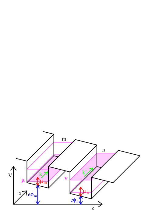
3.3 Sequential tunneling
If the barrier width of a superlattice is large, the structure essentially consists of several decoupled quantum wells. In each quantum well we have a basis set of wave functions , where is the eigenfunction of the quantum well potential. The states have the energy , where the potential energy due to an electrical potential has been considered separately. The notation is clarified in Fig. 10. If the wells are not coupled to each other (infinite barrier width or height) no current flows in the superlattice direction. For finite barrier width the states from different wells become coupled to each other which can be described by a tunnel matrix element in the spirit of [68] inducing transitions between the wells. In lowest order perturbation theory the transition rate is given by Fermi’s golden rule
| (70) |
As the superlattice is assumed to be translational invariant in the -plane, the matrix element is diagonal in . Thus, transitions are only possible if , suggesting sharp resonances when the potential drop between different wells equals the energy spacing of the bound states. This could be nicely demonstrated experimentally in Ref. [114] for simple superlattices and in Ref. [62] for superlattices with a basis where even tunneling over 5 barriers was observed. In the presence of a strong magnetic field along the superlattice direction further peaks due to transitions between different Landau levels are observed [115].
The resonance condition from Eq. (70) implies vanishing electric field for transitions between equivalent levels (in particular the lowest level). As for zero field the current vanishes (provided the electron density is equal in both wells), it was concluded that only phonon-assisted tunneling processes are possible. Thus neither a linear increase of the current for low fields nor a peak at low fields was expected for weakly coupled superlattices [8]. This conclusion is in contradiction with experimental findings [22], where a drift-velocity in qualitative agreement with the Esaki-Tsu result (Fig. 5) has been obtained for weakly coupled superlattices as well. This discrepancy is due to the neglect of broadening in the argument given above.666Broadening had been included in earlier theories [73] but there a term was missing which is essential for the transition between equivalent levels. This point is discussed in Appendix A.
3.3.1 General theory
In a real quantum well the states with energy are not exact eigenstates of the full Hamiltonian due to the presence of phonons and nonperiodic impurity potentials. The respective scattering processes lead to an energy shift and a finite lifetime of the states. These features can be treated within the theory of Green functions (see, e.g., Ref. [65]). While a general treatment is postponed to Chapter 4, a motivation of the concept and a heuristic derivation of the current formula (79) is given in the following.
For a stationary fluctuating potential due to impurities or interface fluctuations one finds
| (71) | |||||
| (72) |
where the second order of stationary perturbation theory as well as Fermi’s golden rule was applied for a stationary fluctuating potential due to impurities or interface fluctuations. For a particle, which is injected at , the time dependence of the wave function is then given by
| (73) |
with , so that . This motivates the meaning of the (retarded) Green function and the (retarded) self energy , which are key quantities in the theory of Green functions. (A nice introduction can be found in Ref. [116].) The Fourier transformation is given by
| (74) |
and the spectral function is defined by
| (75) |
For infinite lifetime one finds which is (except for the factor ) just the contribution of the state to the total density of states. This relation is more general and can be viewed as the contribution of the state if the system is probed with an energy . Here the expressions (71,72) approximately correspond to the Born approximation for . Results for higher order approximations as well as for phonon or electron-electron scattering can be obtained in a systematic manner by the theory of Green functions [65]. Typically becomes a function of energy and momentum, but the structure of Eqs. (74,75) persists.
As the wells are considered to be almost uncoupled, the electronic distribution is described by in each well with the local chemical potential measured with respect to the energy of the lowest level (see Fig. 10). This provides an electron density per energy in the state . Summing all states and integrating over energy, the electron density in well (in units 1/cm2) is given by
| (76) | |||||
| (77) |
with the density of states
| (78) |
in well belonging to the level . Regarding the transitions from level in well to level in well , Eq. (70) is modified as follows:
-
•
The energy is conserved instead of the free particle energy .
-
•
The energy conserving -function is replaced by .
-
•
At each energy the net particle flow from well to well is proportional to () while the net particle flow from to is proportional to (). Therefore the total current is proportional the difference in occupation between both wells. Defining the electrochemical potential it becomes clear that the current is driven by the difference in the electrochemical potential.
Then the current density from level in well to level in well is given by
| (79) |
While the derivation given above is heuristic, a microscopic derivation is given in Sec. 9.3 of [65]. In appendix B.1 it will be shown that Eq. (79) is the limiting case of the full quantum transport theory based on nonequilibrium Green functions in the limit . The same approach has been used for tunneling between neighboring two-dimensional electron gases [117, 118]. It should be noted, that Eq. (79) only holds if the correlations between scattering events in different wells are not significant, otherwise disorder vertex corrections must be taken into account [119].
An important task is the determination of the matrix elements . One possibility is to start with eigenfunctions of single quantum wells and consider the overlap between those functions obtained for different wells . This is the procedure suggested by Bardeen [68] which essentially has been applied in [66, 67] for superlattice transport. Another possibility is to start from the Wannier states (see section 2.3). If a constant electric field is applied to the superlattice structure, the electric potential reads and the matrix elements can be obtained directly from in Eq. (24) or from in Eq. (28). In subsection 3.3.3 it will be shown that the latter Hamiltonian is more appropriate (as already suggested in [73]) by a comparison with experimental data. These matrix elements are calculated for a perfect superlattice structure. Thus they conserve the parallel momentum k. In addition scattering processes at impurities, phonons, or interface fluctuations may cause transitions between different wells. The respective matrix elements can be obtained from the respective scattering potential and the Wannier functions as well. Examples will be given in section 3.3.3, where it is shown that these processes give a background current while the peaks in the current-field relation is typically dominated the k-conserving terms of .
An important feature of Eq. (79) is the fact that the current is driven by the difference of the electrochemical potential in both wells. This is in contrast to the findings of [73] (based on density matrix theory) where the current is driven by the difference where is the occupation of the state . In the latter case the current vanishes for equivalent levels () if the matrix element is diagonal in . In Appendix A it will be shown how the factor is recovered from density matrix theory.
3.3.2 Evaluation for constant broadening
Here we want to derive simple expressions for the current under the assumption of a constant broadening for the electronic states. We assume that only the lowest level is occupied (i.e., ).
First we consider nearest neighbor tunneling with k-conserving matrix elements. Then Eq. (79) can be rewritten as follows:
| (80) |
with
| (81) |
Here the effective field has been introduced and the density of states from Eq. (78) has been applied. Let us assume a constant self-energy in Eq. (81) for the sake of simplicity. Then the spectral functions become Lorentzians . As is essentially zero for energies below we may restrict ourselves to in the evaluation of Eq. (81). For these energies the function takes its maximum at which is larger than zero provided we restrict ourselves to (this is always the case for the resonance and ). In this case the integrand of Eq. (81) does not take large values for and it is justified to extend the lower limit of integration to . A straightforward evaluation using the calculus of residues yields:
| (82) |
which only depends on . Numerical evaluations indicate that these simplifications are quite good for fields above the resonance, i.e. . In the case of and the choice may be better. Note that this simple model with a constant self-energy cannot be used in the calculation of the density of states (78) as the integral for the electron density (77) diverges. Therefore we use the free-electron density of states in the following. With these simplifications Eq. (80) becomes:
| (83) |
with the effective electron density (here )
| (84) |
which describes the difference of occupation in both wells. The electron density is related to the chemical potential via:
| (85) |
Here we assumed that only the lowest level is occupied. The inclusion of higher levels is straightforward, but leads to more complicated expressions. Inserting into Eq. (84) yields:
| (86) |
In the nondegenerate limit limit we have and Eq. (86) is further simplified:
| (87) |
It is interesting to note that the total current can be written as a discrete version of the drift-diffusion model in this case:
| (88) |
with the velocity
| (89) |
and the diffusion coefficient
| (90) |
which satisfy the Einstein relation for . Remember that these expressions only hold for . For the expressions for the opposite direction can be applied.
In the last part of this subsection some explicit results for the current are given. Here we assume equal densities in the wells and set according to Eq. (24).
In the degenerate limit () we find . For we obtain
| (91) |
In the nondegenerate limit we obtain for
| (92) |
In both cases the field dependence is given by the Esaki-Tsu result (34) with .
3.3.3 Results
A variety of calculations for different superlattice structures have been performed within this model. These calculations consist of the following steps:
-
1.
Calculation of the miniband structure and the associated wave functions according to Sec. 2.1.
-
2.
Evaluation of the Wannier-functions and respective couplings , see Sec. 2.3.
-
3.
Evaluation of (intrawell) scattering matrix elements for the dominant scattering processes. For doped superlattices ionized impurity scattering dominates and the respective calculations including screening are presented in [120, 35]. Scattering processes at interface roughness [35] and phonons have been considered as well.
- 4.
-
5.
Determination of the chemical potential for given electron density provided by the donors from Eq. (77).
-
6.
Renormalizing of the matrix elements for each electric field according to Eq. (29).
-
7.
Evaluation of the current density according to Eq. (79).
Results for the superlattice studied experimentally in [123, 124] (9 nm wide GaAs wells, 4 nm AlAs barriers, doping density , cross section ) are shown in Fig. 11. Two pronounced peaks can be identified at low and moderate fields. The low-field peak is due to tunneling between the lowest levels (), while the peak around meV is due to tunneling. While for the dashed line only k-conserving transitions are taken into account, the full line also includes the contributions of interwell scattering matrix elements evaluated for interface roughness, see [35]. (The respective matrix elements for impurity scattering are negligible.) These scattering events represent an additional current channel in Eq. (79) yielding a background current which dominates between the resonances, but is negligible compared to the resonant currents. The height of the peak ( mA) is in good agreement with experimental data exhibiting mA (Fig. 6 of [124]). The low-field peak is not resolved experimentally due to domain formation yielding a current of about 0.076 mA.

Results for the superlattice studied in [31] (15 nm wide GaAs wells, 5 nm Al0.3Ga0.7As barriers, doping density , cross section ) are shown in Fig. 12. The general shape is like the results from the sample mentioned before. While the latter (highly-doped) sample did not exhibit a strong temperature dependence, the situation is different for the low-doped sample considered here. For low electron temperatures K the electrons are located in the impurity band (about 10 meV below the free electron states). Therefore a current exhibits a peak at meV when these electrons can tunnel into the free electron states of the next well. For higher temperatures the electrons occupy the free electron states and the maximum occurs at meV as suggested by Eq. (92). Due to the same effect the peak at meV due to tunneling shifts with temperature. The experimental data (taken at a lattice temperature of 4K) are shown for comparison. While the low-field conductance is in good agreement with the K calculations, close to the first maximum the agreement becomes better for the K curve, which can be caused by electron heating. The heights of both maxima are in excellent agreement between theory and experiment. The difference in position of the second maxima may be caused by an additional voltage drop in the contact, which is not taken into account in the theory, where the field was just multiplied by the length of the sample. Finally, the saw-tooth shape of the experimental current-voltage characteristic is due to the formation of electric field domains as discussed in section 5.

In Fig. 13 results are shown for the superlattice structure from Ref. [125] (25 nm wide GaAs wells, 10 nm Al0.3Ga0.7As barriers, doping density ). Due to the large well width the level seperation is small and several resonances can be observed with increasing field. The calculations (for K and within the approximation (83) applying phenomenological broadenings meV for all levels) have been performed with and without taking into account the renormalization of the matrix elements according to Eq. (29) including the lowest 6 levels. Fig. 13 shows that the result with renormalized matrix elements (full line), see Eq. (28), is in good agreement with the experimental result but exhibits higher peak currents. This may be due to an overestimation of the couplings in the calculation. E.g. assuming barriers of 10.6 nm, the current drops by a factor of 2. An increase of the Al-content in the barriers would give a similar trend.

The results with the bare matrix elements (dashed line), see Eq. (24), deviates strongly from the experimental result. In particular, the peak currents do not increase for resonances at higher fields. This shows that the renormalization procedure is essential if higher resonances are considered.
3.3.4 Tunneling over several barriers
Up to now the discussion was restricted to next-neighbor coupling, which is described by matrix elements in Eq. (28). The extension to tunneling over barriers can be treated analogously taking into account the matrix element . The discussion of Sec. 3.3.2 can be performed in the same way applying the bias drop . Thus we expect resonances at field strengths . The total current is then given by
| (93) |
where the individual current densities are evaluated according to Eq. (79). Here it is assumed that only the lowest level is occupied. For the samples discussed in the last section, as well as for most other samples considered, the respective currents for are negligible. This is different for the sample discussed in [126] (5 nm wide GaAs wells, 8 nm Al0.29Ga0.71As barriers, doping density ), where the second miniband is located around the conduction band of the barrier and the subsequent minibands resemble free particle states. Results of the calculation with , i.e. taking into account tunneling to next-nearest neighbor wells, are shown in Fig. 14.

If the calculation is restricted to the two lowest levels () the current-field relation resembles the findings of Fig. 11. There is a peak at low fields due to tunneling and a peak at meV due to tunneling into nearest neighbor well. The matrix element is small, thus no transitions to the next nearest neighbor well can be seen. This changes completely if the third level () is taken into account for the renormalization of the energy levels and couplings. First the strong coupling to the third level diminishes the value of by 15 meV close to the resonance. Thus the position of this resonance is shifted to meV where the new resonance condition is fulfilled. Secondly a new peak arises at meV due to next nearest well tunneling (remember that the renormalized level energies are field dependent and thus the local field must be taken into account at each comparison). The reason is the strong admixture of (which is quite large for the superlattice structure considered) in the renormalization of the matrix element due to Eq. (29). For the same reason a third peak appears at meV due to tunneling. If the fourth level () is taken into account as well, the result is hardly changed, thus providing confidence into the results. These findings are in agreement with the experiments [126] where a strong increase of the current was observed at field strengths of meV and the current density becomes larger than 0.15 kA/cm2. Nevertheless, no current peak has been observed so far in this field region. Tunneling over more than one barrier has also been observed experimentally in [62, 127]. Current peaks at corresponding to resonances between next neighbors have also been found in the calculation by Zhao and Hone [128]. The hight of these peaks was quite small, probably due to the neglect of interband couplings in their calculation.
These findings show that next-nearest neighbor tunneling is possible in superlattice structures. Nevertheless the quantitative description is still an open issue. The inclusion of results from Zener tunneling [129] may be helpful in future research here.
3.4 Comparison of the approaches
Let us now compare the results from the different approaches miniband transport (MBT), sequential tunneling (ST), and Wannier-Stark hopping (WSH).
MBT-ST: Comparing Figs. 8 and 11 one notices that the global behavior with linear increase of the current for low fields and a maximum at moderate fields is in qualitative agreement for the MBT and ST approach. While the current scales with the square of the coupling for ST, the Esaki-Tsu drift velocity is proportional to . This discrepancy is resolved if either the temperature or the electron density is high and a dependence of the current density is recovered for MBT as well, see Eqs. (46,51). Comparing these results with Eqs. (91,92) we find that the simplified expression become identical for MBT and ST if either or are large with respect to both and . This explains the dependence of the current density observed experimentally in [98, 99] for superlattices exhibiting a rather small coupling meV. As the experiments are performed at K, the estimations (51,92) hold simultaneously and the findings cannot be taken as a manifestation of miniband transport.
ST-WSH: Both approaches exhibit negative differential conductivity for high electric fields. Let us restrict ourselves to the resonance and consider a superlattice with nearest neighbor coupling . For large electric fields the term from Eq. (79) exhibits a two-peak structure
| (94) |
Within the Born approximation for the scattering
| (95) |
Applying the approximation (68) for the expression (79) for the current in the ST model becomes after several lines of algebra
| (96) |
This is the dominating term of the current for Wannier-Stark hopping (65). Thus, the expressions of ST and WSH become identical in the limit of and . This is just the overlapping region between the ranges of validity of both approaches as depicted in Fig. 7.
The transition between WSH and MBT is even more difficult. MBT typically exhibits a behavior for as predicted for the Esaki-Tsu relation, while with various exponents is found for from the WSH model, see Sec. 3.2. As mentioned there, a behavior can be recovered from the WSH approach by summing all contribution in Eq. (64) for . In [110, 113] it is shown that in the field region the results of both approaches agree fairly well. Again this agrees with the joint range of validity depicted in Fig. 7.
4 Quantum transport
In semiconductor superlattices the miniband width , the potential drop per period , and the scattering induced broadening are often of comparable magnitudes. This requires the application of a consistent quantum transport theory combining scattering and the quantum mechanical temporal evolution. Different formulations applying nonequilibrium Green functions [130], density matrix theory [131], the master-equation approach [132], or Wigner functions [133] have recently been used to tackle this general problem for a variety of different model structures.
Here the formalism of nonequilibrium Green functions is applied to study electrical transport in superlattices. This approach allows for a systematic study of both quantum effects and scattering to arbitrary order of perturbation theory. Although the calculations involved are quite tedious (as well as the acquaintance with this method) such calculations are of importance for two purposes: On one hand it is possible to derive simpler expressions like those studied in the preceding section from a general theory, thus shedding light into the question of applicability. On the other hand there are situations where no simple theory exists and thus one has to pay the price to work with a more elaborate formalism.
A variety of different quantum transport calculations for semiconductor superlattices have been reported in the literature: In [134] an analysis within the density matrix theory has been presented, which was simplified to different approaches for low, medium, and high field. The same method was applied to study transport in a perpendicular magnetic field [135]. A similar approach was performed in [136], where the quantum kinetic approach was solved in the limit of Wannier Stark hopping and the nature of phonon resonances were analyzed. The formation of Landau levels in a longitudinal magnetic field causes additional resonances [137]. A transport model based on nonequilibrium Greens function [138] has been proposed as well, although explicit calculations could only be performed in the high temperature limit and within hopping between next neighbor Wannier-Stark states there.
This section is organized as follows: At first the general formalism of nonequilibrium Green functions for stationary transport is briefly reviewed in a form which can be applied to a variety of devices. The special notation to consider transport in homogeneous semiconductor superlattices as well as the approximations used are described in the second subsection. In the third subsection the standard approaches (miniband transport, Wannier-Stark hopping, and sequential tunneling as discussed in section 3) will be explicitly derived as limiting cases of the quantum transport model. This proves the regions of validity given in Fig. 7. Finally, in the fourth subsection results are presented for different samples. The results from the self-consistent quantum transport model will be compared with simpler calculations within the standard approaches applying identical sample parameters. This will demonstrate that the standard approaches work quantitatively well in their respective range of applicability. The reader who is less interested in the theoretical concept and underlying equations may skip subsections 4.1–4.3 and continue with the results in subsection 4.4.
4.1 Nonequilibrium Green functions applied to stationary transport
In this subsection the underlying theory of nonequilibrium Green functions is briefly reviewed. The notation of [39, 65] is followed here and the reader is referred to these textbooks for a detailed study as well as for proofs of several properties addressed here.
We consider a set of one-particle basis states and are the corresponding annihilation and creation operators. The time dependence stems from the Heisenberg picture. Most physical one-particle observables can be expressed by the one-particle density matrix
| (97) |
which is the corresponding quantum mechanical expectation value with the density operator . In particular, the occupation of the state is given by . The task of any many-particle quantum theory is the evaluation of in the presence of a Hamiltonian
| (98) |
where
| (99) |
is diagonal in the basis ,
| (100) |
describes an additional potential term, and refers to interactions with phonons, random impurity potentials (which are treated within impurity averaging), or interactions between the particles.
Within density matrix theory the temporal evolution of is studied directly by applying Heisenberg’s equation of motion for the product . E.g., the time dependence of the occupation is given by:
| (101) |
where denotes the commutator. In order to satisfy the equation of continuity, the particle currents between the basic states have to be identified by
| (102) |
which satisfy as each part of is a Hermitian operator. The scattering induced current can be determined once is specified. This term typically contains higher order density matrices like in the case of electron-electron scattering. Thus there is no closed set of dynamical equations for and the dynamical evolution generates a hierarchy of many-particle density matrices, which has to be closed by approximations, see, e.g., [139, 140] as well as references cited therein.
A conceptually different approach to many-particle physics constitutes the theory of nonequilibrium Green functions which has been developed by Kadanoff and Baym [141] and independently by Keldysh [142]. In this theory the time dependence of and is considered separately, thus two different times appear in the calculation. The corresponding generalization of the density matrix is the correlation function (or ’lesser’ Green function)
| (103) |
which describes the occupation of the states together with the respective correlations both in time and state index. Note the unusual order of indices, which will be helpful in later stages of the theory. The notation follows [39, 65] here. Sometimes (e.g., [141, 143]) the factor is dropped so that agrees directly with the density matrix for equal times. Next to this correlation function the retarded and advanced Green functions are defined by
| (104) | |||||
| (105) |
respectively, where denotes the anticommutator which is appropriate for fermion operators considered here. These functions describe the response of the system at time in state which is excited at time in state .
4.1.1 Temporal evolution
The time dependence of these Green functions is given by the following set equations
| (106) | ||||
| (107) | ||||
| (108) | ||||
| (109) | ||||
which are derived in section 5 of [39]. The same result is obtained from the matrix equations (3.7.5) and (3.7.6) of [65] if the definitions of the retarded and advanced Green functions are inserted.
While the equations for and exhibit a inhomogeneity typical for Green functions, this is not the case for which is, strictly speaking, not a Green function (although this term is often used). The self-energies describe the influence of scattering (compare the simplified description in Sec. 3.3.1). They can be expressed by functionals of the Green functions which depend on the approximation used, such as the self-consistent Born approximation. Here it is crucial to pay attention to the fact that , and belong to the same quantity (a matrix [65] or a self-energy defined on the complex temporal contour [39]) and thus the same approximation has to be performed for each quantity. In this way one obtains a closed set of integro-differential equations, which governs the temporal evolution of the Green functions. On the right-hand side of Eqs. (106,107) the lesser Green functions and lesser self-energies only depend on the time arguments with and due to the properties of retarded and advanced Green functions. Therefore these differential equations for can (at least in principle) be solved explicitly by forward integration.
Equations (106,107) are solved by the integral equation (sometimes called Keldysh relation)
| (110) |
which has a nice interpretation: can be considered as an in-scattering term, which creates a correlated one-particle excitation at times as a result of a scattering event. The retarded and advanced Green functions provide the action of this excitation at the later times and , at which the correlation function is observed. The relation Eq. (110) is a particular solution of the differential equations (106,107). The general solution contains a further term (proportional to the free evolution of without scattering) to satisfy initial conditions, see, e.g., Eq. (5.11) of [39]. Typically, the contribution of these terms decays in time if scattering is present, so that Eq. (110) holds in the long time limit.
If we consider a stationary state without any time dependence of the external potential , all functions depend only on the time difference and it is convenient to work in Fourier space defined by
| (111) | |||||
| (112) |
both for self-energies and Green functions777Different definitions have been suggested which produce gauge invariant equations when is due to a combination of an electric and magnetic field [144, 39]. This is important for various approximations to treat slowly varying fields.. Then the following relations hold:
| (113) |
| (114) | ||||
| (115) | ||||
| (116) | ||||
| (117) | ||||
If and are symmetric matrices, then holds as well. This can be shown by subtracting Eq. (117) from Eq. (116), where and are exchanged.
4.1.2 Self-energies
The self-energies can be obtained from the usual diagrammatic rules which are derived in most textbooks on many-particle theory such as [65]. In the following the results are given within the self-consistent Born-approximation.
For impurity scattering one considers an impurity potential which depends on the locations of the impurities. The respective Hamiltonian is given by
| (120) |
with . For large systems the average over all possible impurity configurations has to be taken (interface roughness can be treated in a similar way). Within the self-consistent Born-approximation only correlations between two scattering matrix elements are taken into account. Thus one finds
| (121) |
For phonon scattering the respective Hamiltonian reads
| (122) |
where are the (bosonic) annihilation and creation operators of the phonon mode (such as acoustic/optical or longitudinal/transverse) with wave vector . Using Langreth rules (section 4.3 of [39]), one obtains the retarded self-energy within the self-consistent Born approximation:
| (123) |
where refers to the phonon Green function. Now we replace the phonon Green function by its unperturbed equilibrium values (section 4.3 of [39] and Eq. (2.9.9)888Note the sign error for in Eq. (2.9.9) of [65] of [65]).
| (124) | ||||
| (125) | ||||
| (126) |
i.e., where is the Bose distribution. As has only poles for , we find
from the residua of the contour over the complex plane with . Putting things together we obtain:
| (127) |
The lesser self-energy reads
| (128) |
which describes the in-scattering from correlated states by phonon absorption as well as stimulated and spontaneous emission of phonons.
The Coulomb interaction can be easily included within the Hartree-Fock approximation, which provides an additional potential (depending on ), see, e.g., chapter 8 of Ref. [38]. Higher order approximations (describing electron–electron scattering) are difficult to implement. All these effects have been neglected in this work.
The combination of these functionals for the self-energies with Eqs. (116,118) for the Green functions provides a coupled set of equations which has to be solved self-consistently to obtain the functions for the stationary state. Afterwards the physical quantities of interest can be evaluated by Eq. (119).
4.1.3 Thermal equilibrium
In thermal equilibrium the electron distribution is governed by the Fermi distribution. In the language of Green functions this can be written as
| (129) |
with the spectral function
| (130) |
which is derived in section 3.7 of [65], e.g.. As discussed before, the occupation of the state is given by
| (131) |
Thus represents the energy resolved density of state . Here it is crucial to note the difference to the classical value of the occupation , which is only recovered in the free-particle case when holds. In contrast and will in general differ, if scattering induced broadening leads to a finite width of the spectral function.
These effects can be estimated assuming and which mimics the fact that there are no scattering states below a band edge at . Then one finds from Eqs. (116,130):
| (132) |
and in the limit one obtains
| (133) |
for a non-degenerate distribution . Thus, the occupation of the high energy states is larger than one would estimate from a semiclassical distribution .
Finally, it should be pointed out, that the different Green functions , , and are related to each other in thermal equilibrium which allows for a description in terms of a single Green function. Thus, the theory of equilibrium Green functions is significantly simpler than its nonequilibrium counterpart discussed here.
4.1.4 Spatial boundary conditions and contacts
Although we are concerned with homogeneous infinite systems in this section, some remarks concerning boundary conditions in real structures are appropriate. They are needed in the discussion of transmission through superlattices [145].
In order to solve the system of equations discussed above in a finite system, boundary conditions have to be specified. Here two types can be distinguished. On the one hand there are regions where the device is terminated by an insulating layer. Here it is appropriate to neglect states in these regions, as their energy is significantly larger than the relevant energies in the device. A far more interesting point is the treatment of contacts, which act as a source or drain for the electric current.
We separate the system into a central region with index and lead region with index . The matrix can than be divided in submatrices of the type , where the index belongs to the central region and to one of the leads. Then the matrix equation (116) can be written in the form
| (134) |
Now let us assume that , i.e., there is no scattering between the lead regions and the central region. Then we can write:
| (135) |
This equation is solved by
| (136) |
where is the Green function of the lead satisfying the equation
| (137) |
It is important to note, that is not exactly the Green function of the pure lead. In fact has to be evaluated from the full Green function and not only from . This difference vanishes under the usual assumption that scattering is negligible in the leads. Now the part of equation (134) for can be written as
| (138) |
This is a closed equation for the matrix concerning the states inside the structure. The term can be viewed as an additional self-energy, due to the transitions between the central region and the lead.
In a similar way Eq. (134) yields:
| (139) |
From Eq. (117) a similar structure as Eq. (134) can be obtained which provides:
| (140) |
Furthermore all relations hold for the advanced Green functions in the same way.
With these ingredients the Keldysh relation(118) can be rewritten as
| (141) |
where defined by
| (142) |
is not exactly the lesser Green function of the pure lead as depends on the full Green function . E.g., this reflects the fact, that the presence of a current through the central region will in principle effect the electron distribution in the lead. Nevertheless this reaction is typically negligible. Again the complications vanish under the assumption, that scattering is neglected in the leads. In the same way one obtains
| (143) |
where Eqs (139,140,141) have been subsequently applied (partially in the form for advanced functions).
Let us consider a typical structure where the central region is connected to several independent leads , which are translational invariant in their current direction. It is assumed that each lead is disorder-free so that the eigenstates can be separated into transverse and longitudinal parts, , where is the spatial coordinate in the direction towards the central structure and is a two-dimensional vector perpendicular to . (A different coordinate system is applied for each lead.) The index numbers the transverse modes within a given lead and denotes the behavior far away from the central region where is assumed. The corresponding matrices are diagonal with matrix elements in this basis.
The electric current from lead and mode into the central region can be obtained from Eqs. (102,119).
| (144) |
where then sum runs over all states belonging to the central region. Eq. (143) provides:
| (145) |
In the second line, the real part was taken by adding the complex conjugated expression (with and exchanged). In the last line the definition
| (146) |
is introduced and it is assumed that the occupation of the modes in the lead can be treated by a distribution function with
| (147) |
Equation (145) has been derived in [146, 38, 39]. Together with Eqs. (138,141) one obtains a closed set of equations for the Green functions in the central regions which is a convenient starting point for the simulation of quantum devices, see. Equation (145) can also be used as a starting point to derive the Landauer-Büttiker formalism [147] which can be easily applied if inside the central region [148]. Otherwise some complications arise as discussed in [145]. A generalization to take into account time-dependent phenomena is straightforward [149].
4.2 Application to the superlattice structure
While the discussion of nonequilibrium Green functions was quite general in the preceding subsection, the general formalism will now be applied to a superlattice structure, which is assumed to be infinitely long. Therefore we restrict ourselves to the central region here. We use the basis given by the products of Wannier states multiplied by plane waves in the direction parallel to the layers, . Then the general states are given by . The Hamiltonian is given by Eq. (23) and is given by Eqs. (24,25). For simplicity we restrict ourselves to the lowest level (and omit the respective indices) and nearest neighbor coupling in the following. Furthermore we set . (The inclusion of higher levels is straightforward but tedious.) We assume that the superlattice is (after impurity averaging) spatially homogeneous in the plane. Then the expectation values must vanish for . Thus the Green functions are diagonal in the wave vector k and can be written as in the following.
4.2.1 Basic equations
The Wannier functions are essentially localized within a single quantum well. Therefore the scattering matrix elements connecting states of different quantum wells are small compared to those describing intrawell scattering. Thus, we restrict ourselves to scattering matrix elements , which are diagonal in the well indices in the following (no interwell scattering).
In this case the scattering-induced currents between different wells vanish in Eq. (102) and the total electric current density well to well is given by
| (148) |
where Eq. (119) has been applied. Similarly the electron density in well is given by
| (149) |
We consider impurity and phonon scattering within the self-consistent Born approximation. Furthermore we neglect correlations between the scattering matrix elements in different wells. This means that vanishes in Eq. (121) for . This assumption is realistic for short range potentials of random impurities but becomes problematic if interface roughness scattering is considered where significant correlations between neighboring wells may occur [150, 151]. For phonon scattering this approximation makes sense if localized phonons such as interface phonons are considered which are different in each well. Under this assumption the self-energies become diagonal in the well index and can be written as
| (150) |
and in the same way for phonon scattering with phonon modes we find from Eqs. (127,128):
| (151) |
and
| (152) |
Then Eq. (116) becomes
| (153) |
and the Keldysh relation becomes
| (154) |
Together with the functionals for the self-energies, Eqs. (153,154) form a closed set of equations which will be solved in subsection 4.4, where explicit results are presented.
4.2.2 Constant scattering matrix elements
For numerical calculations the k-dependence of the self-energy is difficult to handle, as a two dimensional array of has to be evaluated and stored in each calculation cycle. Thus the problem becomes much simpler if constant (i.e. momentum independent) scattering matrix elements are assumed. Then the self-energy for impurity scattering can be written as
| (156) |
which does not depend on k. (Note, that only depends on due to the rotational symmetry in the -plane.) As for large , the respective integral exhibits a logarithmic divergence. This can be either cured by applying a finite cut-off or by adding in the integrand with an arbitrary but constant value . Throughout this work the total scattering rate of free-particle states is used here. This procedure adds a constant real term to the retarded and advanced self-energy, which effectively renormalizes the energy scale to but does not change the physics, which only depends on energy differences.
For free-particle Green functions the integral yields
| (157) |
implying a scattering rate (for )
| (158) |
which will be used as the parameter for the impurity scattering strength in the subsequent calculations.999Note that the product typically does not depend on the sample area .
Phonon scattering is treated in the same way with a constant matrix element . Here the scattering rate is defined via
| (159) |
which is the free-particle spontaneous phonon emission rate if the final state is energetically available and Pauli blocking is negligible at low densities.
4.3 Solution for constant self-energy
The nature of the retarded Green function determined by Eq. (153) can be analyzed by an analytical evaluation for the constant self-energy . Then one finds with Eq. (9.1.27) of [72]:
| (160) |
which is a superposition of broadened Wannier-Stark states, compare Eq. (31). The time-dependent Green function can be evaluated with help of Eq. (9.1.79) of [72]:
| (161) |
This formulation is quite helpful in order to study the different limits. At first one notes that the off-diagonal elements of start to contribute significantly if
| (162) |
Now only the times contribute to due to the exponential decay. If the sine may oscillate over many periods with the average absolute value of . Then Eq. (162) gives . If otherwise we may replace and Eq. (162) gives at . Thus we conclude that the states are essentially delocalized if
| (163) |
On the other hand for
| (164) |
becomes small for and the states are essentially localized. Furthermore for
| (165) |
the poles at are clearly resolved in the energy dependence of Eq. (160) which indicates the persistence of the Wannier-Stark ladder under scattering. The ranges (163,164,165) correspond to the regimes of validity for miniband transport, sequential tunneling and Wannier-Stark hopping, respectively, as given in Fig. 7. In Appendix B it will be shown explicitly that the respective transport equations can be recovered from the model of nonequilibrium Green functions in these ranges.
4.4 Results
Now the results from explicit calculations of the full quantum transport model are presented. Let us first summarize the underlying assumptions as applied successively in subsection 4.2.
-
•
Stationary transport in a homogeneous electric field is considered where only the lowest subband of the superlattice is taken into account.
-
•
The scattering matrix elements are assumed to be diagonal in the well index (no interwell scattering) and no correlations between scattering matrix elements belonging to different wells exist.
- •
Within these assumptions it is possible to solve the system of equations Eqs. (150,151,152, 153,154) self-consistently. Note, that in all these calculations temperature only enters the occupation of the phonon modes, which are assumed to be in thermal equilibrium. The electronic distribution is calculated self-consistently without any assumption of (heated) equilibrium.
Throughout this subsection we use the scattering time ps and the phonon energy meV for optical phonon scattering, which is the dominating energy relaxation process in III-V materials. In order to guaranty energy relaxation for particle energies below 36 meV, acoustic phonon scattering has to be taken into account. We mimic these phonons by a second phonon with constant energy meV. Here should be less than ( meV at 77 K), so that this mechanism can be efficient close to thermal equilibrium. Furthermore the ratio was chosen irrational in order to avoid spurious resonances. The respective scattering time is chosen ps.
At first consider the strongly coupled superlattice studied experimentally in [154]. It consists of 100 periods with 3.45 nm GaAs wells and 0.96 nm AlAs barriers, yielding a coupling meV. The doping density provides and an impurity scattering time ps is applied, which can be estimated from the impurity scattering rate for this doping range [120]. Results for the lattice temperature K (which only enters the phonon occupation number ) are shown in Fig. 15 (full line).

One encounters the typical shape for superlattice transport. While the current peak is in good quantitative agreement with the experimental observation the peak position is shifted significantly. The agreement becomes excellent if a serial resistance of the order of (for the experimental sample area) is included which may result from contacts, leads, or the substrate.
Several simulations have been performed for a model superlattice with meV, nm, and , which has been extensively studied by S. Rott [92] (see also Figs. 8 and 9 in section 3). The rather low doping is taken into account by an impurity scattering time ps in agreement with semiclassical Monte-Carlo simulations. The results for the drift velocity for K and K are shown in Fig. 16 (full line).

For comparison, Monte-Carlo simulations within the miniband transport model (Sec. 3.1) have been performed by S. Rott and A. Markus (Institut für Technische Physik der Universität Erlangen) applying the same scattering matrix elements. For low and moderate field strengths up to meV the relation obtained from miniband transport agrees extremely well with the full quantum transport result. At larger fields, exceeds the miniband width and miniband transport is no longer valid as discussed in subsection 4.3. In Fig. 17 the electron distribution functions (for K) are depicted for various electric field strengths. Comparison of the dashed and full lines for miniband conduction and quantum transport shows that the distribution functions agree very well for meV in the energy range meV. For higher values of the quantum mechanical distribution function is larger than its semiclassical counterpart. Here the occupation is quite small, so that the tail from the broadened spectral function becomes visible [156, 157], in good agreement with the estimate of Eq. (133). In compensation the quantum result is slightly smaller than its semiclassical counterpart for low values of , as the total density has to be the same. Nevertheless, these effects are small compared to the typical occupation numbers and one can conclude that the Boltzmann equation for miniband transport gives reliable results both for the current density and the electron distribution. Actually, the quality of agreement is stunning regarding the crude assumptions necessary for the derivation of the Boltzmann equation in Appendix B.2.
The velocity-field relations from Fig. 16 can be directly compared with those in Fig. 8, where the correct matrix elements have been applied within the semiclassical miniband transport model. There are no qualitative differences, so that one may conclude that the assumption of constant matrix elements as well as the artificial acoustic phonons do not cause unphysical results.

Let us now study the details in the velocity-field relation and through a glance at the respective distribution functions. At very low fields one encounters a linear increase of the drift velocity with the electric field. Here the distribution function resembles a thermal distribution with the lattice temperature (dotted lines for meV). The slight shift can be easily treated within linear response, yielding a field-independent mobility.
For higher fields ( meV) one encounters a sublinear increase of the drift velocity. Here significant heating occurs, which can be seen from the respective distribution function in Fig. 17. The distribution functions resembles a shifted Fermi distribution with an electron temperature K for . For higher energies optical phonon scattering is still efficient and one encounters a steeper decrease of with energy. This shows that the concept of an electron temperature makes sense in this range both for quantum and semiclassical transport even without electron-electron scattering. For electric fields close to the current maximum ( meV) the distribution functions strongly deviates form any thermal or heated distribution function. In the semiclassical picture this can be viewed as a result from frequent Bragg-scattering where particle reach the states with . If the electric field becomes even stronger, the electrons may traverse the -Brillouin zone several times without scattering for in the semiclassical miniband picture. This leads to a flat electron distribution in as can be observed for meV in Fig. 17. The same holds for the quantum distribution function although the reason is different. In this field range () the Wannier-Stark states are essentially localized to a single well. Thus a semiclassical occupation of the Wannier-State creates a flat distribution in -space as well.
While both approaches explain the flat distribution in -space, significant differences in scattering arise. The electron running through the states exhibits different energies during passage. This provides different selection rules for scattering then the presence of a Wannier-Stark states with fixed energy. Therefore the -distribution calculated by the quantum transport model exhibits pronounced features on the energy scales and as well as the difference because at these energies new scattering channels appear. If these scales match, the phonon resonance at appears in the velocity-field characteristics, see Fig. 16. In contrast, the semiclassical result exhibits a rather flat distribution and no phonon resonance can be observed.
The situation changes for small coupling and strong scattering, when holds. Fig. 18 shows the velocity field relations for meV and ps. Here the semiclassical miniband transport calculation strongly deviates from the full quantum result both in the low-field and in the high-field region. Nevertheless, the agreement gets better for higher temperatures.

In Fig. 19 the quantum transport calculations are compared with results from the models of Wannier-Stark hopping and sequential tunneling. In all calculations identical scattering matrix elements are used. The calculations for Wannier-Stark hopping have been performed by S. Rott and A. Markus (Institut für Technische Physik der Universität Erlangen) using self-consistent distribution functions, see section 3.2 for details. One finds that the Wannier-Stark hopping model provides good results (including the phonon resonance) in the high-field region where ( meV and 15 meV for the left and right superlattice, respectively, for energies at which phonon emission is possible). The agreement deteriorates significantly if the simple version of Wannier-Stark hopping without self-consistency is applied.

The sequential tunneling model clearly fails at low and moderate field strengths for the strongly coupled superlattice (left part of Fig. 19) as . In the high field region the results becomes valid and the phonon resonance can be observed within the sequential tunneling model. For weakly coupled superlattice (right part of Fig. 19), the sequential tunneling model should be applicable and the low-field conductance is in good agreement with the full quantum transport result. Significant deviations occur at intermediate fields because electron heating is not included in the sequential tunneling model. As the current density drops with electron temperature (see section 3.3.2), the drift velocities are too high, if heating is neglected. These heating effects have been recently taken into account within the sequential tunneling model [158, 159].
In Fig. 20, a comparison between quantum transport and sequential tunneling is shown for the weakly coupled superlattice studied in [123, 124], see also section 3.3.3. Excellent agreement is found between both approaches and the results agree well with those presented in Fig. 11 applying realistic impurity scattering matrix elements and neglecting phonon scattering.

The observations presented here correspond to the boundaries of validity given in Fig. 7, which can be considered as a reliable guide. Furthermore the results indicate that the models of miniband transport and sequential tunneling give qualitatively reasonable results even outside their range of applicability. Thus they can be used as a rough guide to obtain a correct order of magnitude of the current.
5 Formation of field domains
As shown in sections 3 and 4, semiconductor superlattices typically exhibit ranges of negative differential conductivity. This occurs after the first current peak for miniband transport (or sequential tunneling) as well as after the subsequent resonances at higher fields when different levels align. The shape of the current-field relation is thus typically of N-type and domain formation effects are likely to occur (see [45] for a general overview). The prototype of an extended device with N-shaped current-field relation is the Gunn diode which exhibits self-sustained current oscillation due to traveling field domains [160, 161, 162, 163, 164, 165, 166]. A similar behavior has been suggested for semiconductor superlattices [18, 167], and oscillatory behavior has indeed been found experimentally in the last years [19, 168] with frequencies over 100 GHz [20, 169]. In contrast to the Gunn diode, semiconductor superlattices frequently exhibit the formation of stable stationary domains which lead to a characteristic saw-tooth pattern in the current-voltage characteristic (see Fig. 21a) as observed by many different groups [16, 17, 123, 124, 170, 171, 172, 173, 174]. (See also [175, 176] for domain formation in a parallel magnetic field.) The measurements are typically performed by applying a continuous sweep of the bias. As the branches overlap, one observes different parts of the branches for sweep up and sweep down of the bias101010Ofcourse the variation of the bias must be slow, so that the field domains can follow adiabatically. Otherwise, the sawtooth structure disappears [177, 178]. Sometimes a quite complicated behavior is observed as well. In particular for the superlattice structure of Fig. 21 stationary field domains [179], self-sustained oscillations [19], as well as bistability between stationary and oscillatory behavior [180] has been observed under fixed bias conditions within the first plateau of the current-voltage characteristic.


(a) (b)
In this section such complex behavior will be analyzed by a comparison between numerical results based on the sequential tunneling model from section 3.3 with analytical studies. It will be shown that most of the observed effects can be understood as the result of a competition between two mechanisms: (i) The motion of fronts connecting low- and high-field domains and (ii) the dynamical evolution of the field close to the injecting contact, i.e., the cathode.
This section is organized as follows: First a model is described which is able to reproduce most of the experimental findings for weakly coupled superlattices. In subsection 5.2 numerical results are presented reproducing the behavior shown in Fig. 21. In the subsequent subsections the key elements, namely the traveling fronts (subsection 5.3) and the cathode behavior (subsection 5.4) are discussed separately. In subsection 5.5 it will be demonstrated how their combination explains the behavior observed both in experiment and simulation. Finally, the findings are summarized and an instruction for the analysis of nonlinear superlattice transport behavior is presented.
5.1 The model
In weakly-coupled multiple quantum wells the electronic states are essentially localized in single wells forming energy levels . Transport then occurs by sequential tunneling between neighboring wells. The current from well to well is modeled by a function , where is the average field drop between the respective wells and denotes the electron density (per unit area) in well as depicted in Fig. 22.

Considering a superlattice with wells embedded between barriers, the dynamics is determined by the continuity equation
| (166) |
The electric field satisfies Poisson’s equation
| (167) |
where is the doping density per period (per unit area), and and are the relative and absolute permittivities. Finally, the total voltage is determined by
| (168) |
where we have neglected a possible voltage drop at the contacts for simplicity. Equations (166-168) can be transformed into an equivalent set of equations:
| (169) | ||||||
| (170) | ||||||
| (171) | ||||||
This shows that the dynamical evolution of the local fields is driven by the total current density , which itself is determined by the global behavior of the sample. Thus, represents a global coupling. In order to obtain a closed set of equations, the currents across the first (cathode) and the last (anode) barrier, and , respectively, have to be specified. Here the following approaches have been taken previously:
In [66, 182, 183, 184] these contact currents were calculated within the assumption of two fictitious additional wells, one before the first and one after the last barrier. Then the current is given by for tunneling between two wells, where the fictitious density has to be specified, usually assuming , with . The current across the last barrier is treated analogously by introducing a fictitious density . This approach will be referred to as constant density boundary condition in the following.
Alternatively, one may assume that the current is proportional to the local field, i.e., with an Ohmic conductance . For the anode condition one has to take into account, that the current must vanish if tends to zero, as otherwise the density can become negative. This can be ensured by an additional factor and is a reasonable choice. This will be referred to as Ohmic boundary condition.
The actual potential distribution at the boundary could be taken into account within a transmission-type formalism [67]. Here I will restrict myself to the two approaches sketched above, which are simpler and provide an understanding of most of the underlying physics. They contain the main ingredients to understand more complicated and physically better motivated versions.
5.2 Numerical results
Let us consider the GaAs/AlAs superlattice structure from Fig. 21 (which exhibits a rather small miniband width of meV) as a model system for the subsequent calculations. In the following the function is calculated from the nominal sample parameters by the model described in section 3.3. (See also Fig. 11.) The result for a homogeneous electron density is shown in Fig. 23. Here, the current is shown applying the experimental sample area in order to facilitate comparison with experimental data. In this section the factor is included, so that the sign of the current equals the particle current in transport direction which simplifies the following discussion. Fig. 23 shows that the current-field characteristics exhibits a linear conductivity for low fields, a maximum at , a range with negative differential conductivity for and a second sharp rise of the current for higher fields due to resonant tunneling from the lowest level to the second level of adjacent wells.

Different approaches to obtain the local current density can be applied as well and the overall results do not depend on this choice, provided the general shape resembles Fig. 23. E.g., in Refs. [19, 66, 67, 182, 174, 185] one can find similar results like those presented in this section, where varios types of local current density functions are applied.
By simulating equations (166-168) for a fixed bias until a stationary state is reached the stationary current-voltage characteristic shown in Fig. 24 are obtained. Here the initial condition for the calculation is taken from the result of the previous voltage point, simulating a sweep-up of the bias . In Fig. 24a we use the constant density boundary condition with , while the Ohmic boundary condition with mA/V was applied in Fig. 24b. Both characteristics are almost identical and in reasonable quantitative agreement with the experimental data presented in Fig. 21a. As shown in the insets, the branches are due to the formation of electric field domains inside the sample, where a low-field domain is located at the cathode and a high-field domain is located at the anode. Close to the contacts we find a small transition layer, which depends on the contact boundary conditions. The domain branches span a fixed current range with A and A, indicated by the hatched area in Fig. 23.

For different boundary conditions oscillatory behavior can be obtained for the same sample parameters. This is shown in Fig. 25 for the Ohmic boundary condition with mA/V. The current signal resembles the measured signal displayed in Fig. 21b. Nevertheless different current signals have been observed as well, both experimentally and in numerical simulations (see, e.g., Fig. 10.12 in [35] for results obtained from the same model with different boundary conditions). The oscillations reported here are due to traveling high-field domains which is different from the calculations presented in [181, 186, 187] where traveling monopoles have been reported. This is due to the difference in the boundary conditions and in the transport model used in both calculations, see also Refs. [185, 188], where this point is analyzed.
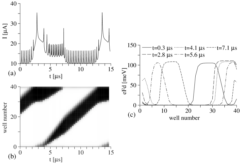
5.3 Traveling fronts
In this subsection traveling fronts will be examined which will form one of the building blocks to understand the global dynamics. Eq. (169) shows that the dynamical evolution of the electric field is determined by the total current . The corresponding dynamics can be studied most easily for a constant total current corresponding to current controlled conditions. For A A we have three intersections of with the homogeneous current-field relation shown in Fig. 23. They correspond to three stationary homogeneous field distributions . Linearization of Eq. (169) shows that the field is unstable under current-controlled conditions as . Thus a homogeneous initial field distribution will either tend to or to in its temporal evolution.
For an appropriate inhomogeneous initial field distribution a part develops to while another part reaches . Thus a front between these two spatial regimes appears. Calculations on the basis of Eqs. (169) - (170) show that the front develops on a typical time scale of less than s and afterwards travels through the sample with unaltered shape, as shown in Fig. 26.

Here two types of fronts appear. Accumulation fronts connect a low-field region on the left side to a high-field region on the right side as shown in Figs. 26a,26c. Eq. (170) shows that the carriers accumulate () in the transition region. If, on the other hand, the high-field region is located on the left side, see Figs. 26b,26d, a depletion front is present.
As can be seen from Fig. 26 the front velocities depend on the external current and differ for accumulation fronts with velocity and depletion fronts with velocity . These velocities have been determined from a series of simulations as a function of and are given in Fig. 27. Note that becomes zero in a finite range of currents corresponding to the range of the stationary domains discussed above. (Such a stationary front is shown in the inset of Fig. 24.) For higher currents is negative, i.e., the front travels upstream against the direction of the average drift velocity of the electrons as shown in Fig. 26c. In contrast is positive for all currents for the sample parameters used. These functions have been shown to be very helpful to understand and analyze Gunn oscillations [166, 189]. Here they are applied in the context of semiconductor superlattices where some peculiarities can be found.

In the following two subsections the special shape of and will be explained.
5.3.1 Continuum limit and fronts traveling backwards
In order to understand the simulations, let us first discuss the continuum limit of vanishing superlattice period. We can approximate
| (172) |
with the average drift velocity and an effective diffusion constant given by
| (173) |
This approximation becomes exact in the nondegenerate limit, see Eq. (88), which is not applicable for the sample discussed here. Replacing finite differences by derivatives, Eqs. (169,170) are transformed to
| (174) |
This is the standard equation for the Gunn effect, for which and holds [163]. Neglecting diffusion, the fronts can only travel in the direction of the drift velocity, i.e. , which can be shown by the method of characteristics [190]. We conclude
In contrast, if the drift term is neglected, one obtains a nonlinear reaction-diffusion system. Here solutions of traveling accumulation fronts exist with a monotonic function f(z) and and . Furthermore one finds if where
| (175) |
see section 2 of [191]. The depletion fronts can be obtained applying the symmetry operation , thus . Typically, the integral is positive for and negative for , where is the current, where both field domains coexist. (This value satisfies the equal area rule [192] .) Then one finds the generic scenario:
Including the drift term, it is obvious that both velocities will increase and the intersection point is shifted to a positive velocity in agreement with Fig. 27. If the diffusion constant is not too small, a range of negative velocity is likely to remain. This can be estimated in the following way: Let satisfy . Linearization of Eq. (174) for gives the dispersion
| (176) |
with , , and the dielectric relaxation rate . Thus an initial condition has the solution
| (177) |
which essentially travels in the direction of the drift velocity. Nevertheless also grows exponentially in the range provided . This can be interpreted as the occurrence of an absolute instability [193] for
| (178) |
when a local perturbation from a homogeneous field spreads in both directions. If is larger than the bound given by (178), spatial variations not necessarily travel through the structure and either stationary domain structures or backward traveling field domains are likely to occur. This condition has been applied to superlattice transport in [194] and seems to be in good agreement with data from a variety of strongly coupled superlattices [195]. Nevertheless the condition for a stationary front () is only valid for a specific current, as the functions are strictly monotonic for the continuous drift diffusion model (174). This is in contrast to the results shown in Fig. 27 where is zero in a finite interval. Thus we can draw the following conclusions from the continuum limit:
-
•
Backward traveling fronts can occur for large values of both for accumulation and depletion fronts.
-
•
The front velocities are decreasing with for accumulation fronts and increasing for depletion fronts.
Finally note that the simple model for the current used in [181, 182, 184] (where the -dependence of is neglected) implies in Eq. (172). These models are appropriate for the second plateau but differences occur for the first plateau discussed here. In particular these models cannot reveal fronts traveling backwards.
5.3.2 Discreteness of the superlattice and stationary fronts
While the considerations of the previous subsection apply to a continuous system, weakly-coupled superlattices form a system where the discretization due to the finite superlattice period is essential. As explained in [35, 184, 196] this leads to stationary domain states, provided the transition region between the two domains becomes of the order of the superlattice period. In this case the accumulation or depletion front gets trapped within one well. As this pinning can occur within a certain range of currents one observes extended branches in the current-voltage characteristic (Figs. 21,24). As shown in [35, 184] the sufficient condition for a stationary accumulation front reads
| (179) |
(Similar results have been given in [182, 183, 196] as well.) For the superlattice structure considered, one obtains cm2, which is smaller than the actual doping density cm2. Therefore stationary accumulation fronts can exist in a certain range of currents for this sample. Let us remark that the condition (179) strongly resembles (178) if the diffusion constant for shot noise [194] is used. Again the discreteness of the structure is responsible for the occurrence of stable domains.
For more strongly doped superlattices the velocity of the depletion fronts may become zero as well. The corresponding condition is given by [35]
| (180) |
For the superlattice structure considered this relation give cm2, which is larger than the actual doping. Therefore no stationary depletion fronts occur in this sample. Together with the monotony arguments depicted in the previous subsection these estimations explain the shape of the functions shown in Fig. 27. Rigorous proofs of some of the features discussed here are given in [197].
In general one can distinguish three types of superlattice: For there are no stationary fronts. For accumulation fronts are stationary within a certain current range. Finally for highly doped superlattices with both accumulation fronts and depletion fronts can be stationary, i.e., pinned at a certain well.
5.4 The injecting contact
Now the influence of the contact boundary condition at the cathode shall be investigated which is essential for the dynamical behavior. For a given current , the evolution of the field at the cathode, , is given by:
| (181) |
Let be the solution of , which forms an attracting point of Eq. (181), i.e., . Then will tend towards . Provided the relaxation time at the contact is much smaller than the corresponding time scale on which changes, one may use the boundary condition to describe superlattice dynamics. If is close to the value of or , a low-field domain or a high-field domain will be injected into the sample, respectively [190]. For a pure drift system the condition for the injection of a low-field domain is given by [45]. This gives a qualitative bound but this does not hold strictly in the superlattice system due to discreteness and diffusion. For the Ohmic boundary condition depicted in Fig. 23 we thus find that a low-field domain forms close to the injecting contact for and a high-field domain forms there for , where is the current at the intersection of with the homogeneous current-field characteristic.
In contrast to the cathode where electrons are injected into the sample, the anode contact conditions do not play a major role. A boundary layer exists there, which is typical stable (see e.g. [190] for a discussion within a drift model). This can be understood from the fact, that the perturbations mainly travel through the sample in the direction of the current flow, see Eq. (177), even if there might be some response in the opposite direction as well.
5.5 Global behavior
The behavior found numerically in Sec. 5.2 will now be explained within the interplay between the dynamics of fronts and contacts. Let us restrict ourselves to rather long superlattices where the criterion
| (182) |
is satisfied so that the homogeneous field distribution is unstable [161, 162]. In this case either stationary domain states, self-sustained periodic current oscillations, or aperiodic behavior occur. Calculations yield cm2 for the superlattice structure under consideration, which is much smaller than . This criterion has been successfully applied to a variety of superlattice structures [195].
5.5.1 Formation of stable stationary field domains
For the sample considered, accumulation fronts become stationary in the current range . Obviously, these domain states are only possible if the low-field domain is maintained at the cathode, i.e. , as discussed in the previous subsection. For mA/V, we find A. Thus these domain states are allowed in agreement with the numerical findings from Fig. 24. The same behavior can be found for the constant density boundary condition with . In this case the field remains in the low field region as long as , which is hardly exceeded unless the superlattice is operated in the second tunneling resonance. Therefore similar behavior is observed for both boundary conditions.
For the superlattice structure considered here, stationary depletion fronts do not occur. Therefore one expects that the high-field domain is always located at the anode for stationary behavior. This agrees with experimental findings for this superlattice [198]. For superlattices with a higher doping the situation is different and field distributions have been observed where the high-field domain is located at the cathode [172]. These experimental findings are in good agreement with the criterion (180). Simulations [122] give such a field distribution for appropriate contact conditions. A further example is shown in Figs. 28c,d.
These stationary fronts appear within a finite current range . If the maximum accumulation occurs in well , the total bias for accumulation fronts is given by
| (183) |
Here and are correction terms due to the inhomogeneous field profiles at the contacts and in the front region, which do not depend on the front position , provided this position is not to close to either of the contacts. Due to the periodicity of the superlattice, a shift of the front by one period does not change the current. Thus, one obtains up to branches of Eq. (183) with . This results in the characteristic sawtooth pattern in the current-voltage characteristics for Figs. 21a,24. In addition, two field distributions exist, which exhibit a homogeneous (except for boundary effects) field distribution and for all . The actual number of branches can be smaller due to the inhomogeneous field distributions at the boundaries as shown in the insets in Fig. 24. The voltages corresponding to neighboring branches differ by . As this difference depends on the current, these branches are not exactly reproduced for different , but change their shape. Neglecting boundary effects, their slopes are given by
| (184) |
which varies between for small biases (accumulation front close to the right contact) and for large bias (accumulation front close to the left contact). The behavior for depletion fronts is identical except that they are located close to the left/right contact for small/large bias and the fields and have to be exchanged in Eq. (183).
5.5.2 Self-sustained current oscillations
For mA/V we find A, which is smaller than . Therefore no stationary domain states are possible. In contrast, self-sustained oscillations occur, as shown in Fig. 25. The mechanism of these oscillations can be understood by using ideas reminiscent of the Gunn effect asymptotic [166]: for s the total bias is distributed between a high-field domain and a low-field domain. As the total bias is constant, there is a certain part of each oscillation period during which both boundaries must travel at the same velocity [166, 189]. Then giving mA (see Fig. 26). As the cathode remains in the the low-field domain. We observe a current signal which is constant in average and exhibits fast oscillations with the period due to well-to-well hopping of the accumulation front. This feature has been discussed in the analysis of switching behavior [199, 200, 201] and is explained in detail in [185].
After the leading edge of the high-field domain has reached the anode, the size of the high-field domain shrinks as the trailing edge travels further with unaltered velocity. In order to maintain the total bias, the fields increase in both domains, leading to an increase of via the global condition (171), as can be seen at s. When becomes larger than the field at the cathode injects a high-field domain into the superlattice (s). As is quite large in this range of currents the newly formed domain expands relatively fast and the fields drop in order to maintain the bias. Therefore the current shrinks again below and the cathode injects a low-field domain into the superlattice (s).
In this situation three boundaries are present in the superlattice. The old accumulation front (around well 35) and the depletion and accumulation front limiting the newly formed high-field domain (from well 5 to 10). In this situation the sum of the extensions of both high-field regions is kept constant if the depletion front travels with twice the velocity of the accumulation fronts, i.e. yielding mA (see Fig. 26). This is just the average current observed in the simulation observed in the plateau around s. The oscillatory part of the current exhibits a lower fundamental frequency compared to the frequency observed around s as . In addition one observes two peaks per period resulting from the presence of two accumulation fronts. This behavior is maintained until s when the old accumulation front reaches the anode and only the newly formed high-field domain remains. Afterwards the cycle is repeated.
Different scenarios for oscillatory behavior are also possible. For the constant density boundary condition with oscillations due to traveling depletion fronts have been found for the same model, see Refs. [181, 35] and Fig. 29d for a further example. In this case the field at the cathode remains above , once this range of fields has been reached. For the high-field domain cannot extend over the whole superlattice and thus a range of fields with must be present. This requires the existence of a depletion front, which cannot be stationary for the superlattice considered here as . Thus the front travels towards the anode increasing the width of the high-field domain. In order to keep the bias constant, the field inside the domain shrinks during this process. If becomes lower than the domain becomes unstable and the field tends to the low field value . As the field remains high due to the boundary condition a new depletion front is formed and the cycle repeats itself. An equivalent oscillation mechanism is discussed in detail in [181, 190] for accumulation fronts. (This mechanism is also active in the oscillation shown in Fig. 30b.) It becomes relevant for lower doped samples, i.e., for , when these fronts cannot become stationary.
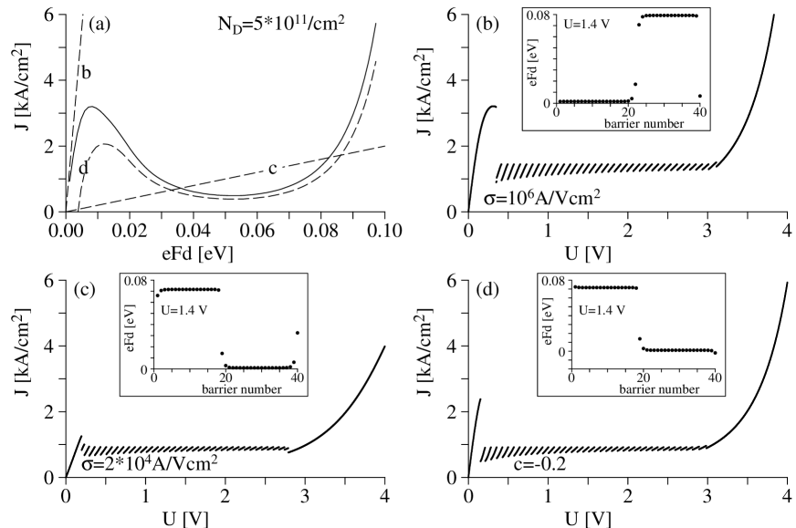
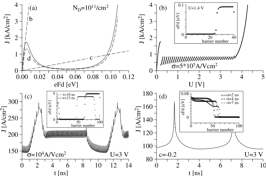
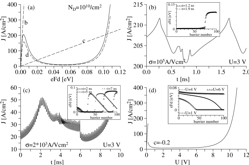
5.6 Summary
Let us summarize the findings from the previous subsections in order to obtain a general outline for the analysis of semiconductor superlattices. To visualize the general trends, various types of behavior are shown for a superlattice test structure in Figs. 28–30 for different doping densities.
- 1.
- 2.
-
3.
Compare theses quantities with the actual doping density
- :
-
Stable domains form both for good and bad contacts at the cathode. The domain boundaries can be formed by accumulation layers, see Fig. 28b, or depletions layers, see Figs. 28c,d. Both may even coexist if the respective ranges overlap. In all cases the current-voltage characteristic exhibits the typical saw-tooth behavior, where the number of jumps roughly equals the number of periods.
- :
-
The behavior depends crucially on the boundary condition at the injecting contact: If the current can be injected at a fairly low electric field in the cathode (good contact), stable domains are found which exhibit accumulation layers, i.e., the high-field region is located at the anode, see Fig. 29b. Otherwise, for bad contacts, one observes self-sustained current oscillations, see Figs. 29c,d. The shape of these oscillations as well as their frequency depends on the type of contacts.
- :
-
Stable domains associated with a saw-tooth current-voltage characteristic do not occur. The behavior of the sample is either dominated by current oscillations, see Figs. 30b,c or a rather smooth stationary current-voltage relation, see Fig. 30d. According to the -criterion (182), the latter case dominates for short samples and lower doping. Here it seems to be crucial that the inhomogeneous field distribution essentially takes values from a range where is small, suggesting large values of . (Similar behavior is found for A/Vcm2 if the number of periods is reduced.)
Experimentally, this scenario can be verified by varying the electron density by optical irradiation [202, 203]. Transtions between oscillating and stationary domains can also be provoked by changing the lattice temperature [204]. This effectively alters the shape of the relation and thereby via Eqs. (179,180) the critical doping densities. There are several further aspects complicating the picture sketched above, which are not addressed in the discussion given here:
Real superlattices are not perfect structures, where the properties of each well are repeated exactly. In contrast there will be fluctuations in the doping density, the barrier and well width as well as the material composition from period to period. Some information can be obtained by X-ray analysis and indeed it has been possible to relate some global properties to the extend of disorder [195, 205] in the respective samples. By extensive simulations it has been shown that the presence of such disorder inside the superlattice affects the behavior significantly [187, 206]. The nature of the current oscillations, the actual shape of the domain branches, as well as critical doping densities can be affected by the amount of disorder. Frequently, one observes a direct correlation between some global current signals and the actual realization in a particular sample [159, 207].
Recently, an additional S-type current-voltage characteristics has been found in strongly coupled superlattices due to electron heating [208]. The combination of N-type and S-type negative differential conductivity may provide additional interesting effcets.
In all calculations performed here the transport model for sequential tunneling has been applied, which provides rate equations between the quantum wells. For strongly coupled superlattices it is questionable if the electrons can be confined to accumulation layers extending over a few wells. Therefore it is not clear, in how far these stationary domain structures persist. The alternative is to start from the miniband model. Such calculations have been performed in [209, 210] using the drift velocity from the relaxation time model. A more microscopic approach can be performed within the hydrodynamic model [167, 211]. Nevertheless one has to be aware that the miniband transport model becomes questionable for large field strengths (compare Fig. 7), which are typically reached within a high-field domain. Thus a quantum transport calculation would be desirable to clarify the situation. Except for the stability analysis of the homogeneous state with respect to spatial fluctuations in [138] I am not aware of any quantum transport simulations concerning inhomogeneous field distributions in superlattices111111Very recently stationary inhomogeneous field distributions could be modeled for short superlattices within the quantum transport model discussed in Section 4. First results are in qualitative agreement with those from the sequential tunneling model [212].. Thus it remains an open question in how far quantum effects modify the behavior discussed in this section.
6 Transport under irradiation
In this chapter we consider superlattice transport under irradiation by an external microwave field with frequency . In this case a further energy scale, the photon energy of the radiation field, comes into play. For frequencies in the THz range (1 THz meV) this energy is of the same order of magnitude as typical miniband widths, scattering induced broadening, and the potential drop per period. This provides an interesting field to study various types of quantum effects.
Transport under irradiation has first been studied theoretically within the simple Esaki-Tsu model. In this context it was shown that negative differential dynamical conductance [5, 213] occurs. In the rectified response replica of the current peaks appear at field strengths obeying (with ) indicating the quantum nature of the radiation field [100, 214]. Furthermore absolute negative conductance (i.e. a negative current for positive bias) is possible under certain conditions [215, 216].
With the development of the free-electron laser as a high power THz source it became possible to study these effects experimentally and indeed the photon-assisted replica of current peaks [217, 218] as well as absolute negative conductance [31] were observed. The superlattices used in these experiments exhibited rather small miniband widths, so that the application of miniband transport (as done in the theories mentioned above) is questionable as discussed in chapters 3 and 4. Nevertheless, these findings could be explained qualitatively [31, 219, 220, 221] within the standard theory of photon-assisted tunneling [222, 223, 224] as well, which is applicable for sequential tunneling. A quantitative description of these experiments [120] was possible within the sequential tunneling approach described in Sec. 3.3.
Photon-assisted peaks in the current-voltage characteristic could also be observed in strongly coupled superlattices [225] although the results are less clear in this case. Furthermore the reduction of current due to the irradiation could be nicely demonstrated in experiments for superlattices with large miniband widths [226], which gave an excellent agreement with the simple miniband models mentioned above.
In this section the basic ingredients of the transport theory under irradiation are reviewed. The first subsection deals with the simple quasi-static response, which holds for low frequencies. This will be the basis for the discussion of quantum effects in the subsequent subsections. The main results within the miniband transport will be reviewed in the second subsection. Here a form will be chosen which simplifies the comparison with sequential tunneling which is discussed in the third subsection.
Throughout this chapter we consider a homogeneous electric field along the superlattice structure which can be separated into a dc-part and a cosine-shaped time dependence with amplitude , i.e.,
| (185) |
The transport problem has been considered for in the preceding chapters where the relation was obtained. Now we are looking for periodic solutions with period , neglecting transient effects as well as the possibility of aperiodic behavior. Then the general current response can be written as
| (186) |
In general, four different aspects of transport under irradiation can be identified:
-
1.
The rectified response is considered in many different experiments. It is easily accessible and can be used for the detection of high frequency signals.
-
2.
The active current provides the direct interaction with the irradiation field. If we observe gain at the given frequency .
-
3.
The reactive current describes the response out of phase, which can be described by an inductance () or a capacitance () in standard circuit theory. There are two possibilities to define inductive and capacitive effects: (i) One assumes that and are always positive. Then positive/negative is referred to as an inductive/capacitive effect, respectively [227]. (ii) One regards the low frequency limit. It will be shown later that typically for low frequencies. This resembles the behavior of a capacitor which can either be positive or negative [228].
- 4.
In this chapter we restrict ourselves to homogeneous field distributions with the time dependence (185). In this case the current is homogeneous over the superlattice direction and no charge accumulation inside the structure occurs. Such complications can be treated within the general formalism discussed in [232, 233]. Domain formation effects in superlattices under irradiation have been studied in [234]. If higher harmonics are present in the time dependence of the field, the superlattice may act as a rectifier [235]. Furthermore the response of an external circuit is neglected here. A detailed discussion of the latter issue can be found in [236].
6.1 Low frequency limit
In the range of radio frequencies (say THz) the frequency is slow with respect to the internal degrees of freedom, such as carrier heating or (where describes typical energy scales of the transport problem). Than one can assume, that the current follows the field instantaneously:
| (187) |
This shows that all terms vanish in the radio-frequency limit. Furthermore, we obtain the following expressions in lowest order of the irradiation field:
| (188) | |||||
| (189) | |||||
| (190) |
They will be compared with the results discussed in the next subsections.
6.2 Results for miniband transport
In the miniband transport model the time dependence of the electric field enters the Boltzmann equation (35) which complicates the problem tremendously. The easiest way to deal with this situation is the relaxation-time approximation. Assuming , Eqs. (54,56) can be solved for an arbitrary time dependence of the electric field. One obtains [215, 237]
| (191) | |||||
| (192) |
Let us now consider the field dependence (185). The crucial parameter in the following will be the ratio between the ac-field strength and the photon energy
| (193) |
which will appear in most of the following results as the argument of the integer Bessel functions . In order to avoid confusion with the symbol for the current density, the results are given in terms of the current in the following. Then one finds:
| (194) |
From Eq. (57) one can identify
| (195) |
with . Furthermore we define
| (196) |
where the Kramers-Kronig relation, connecting the imaginary and real part of , has been applied. Then we can evaluate the components of Eq. (186) in the form
| (197) | |||||
| (198) | |||||
| (199) |
Let us first consider the rectified response , which is a sum of several dc-curves (as shown in Fig. 5b shifted by integer multiples of the photon energy. This explains the occurrence of photon-assisted peaks at biases as shown in Fig. 31a. If the coefficient for becomes small, i.e., close to a zero of (the first zero occurs at ) the terms with dominate, which can provide absolute negative conductance for as shown in Fig. 31b [216].
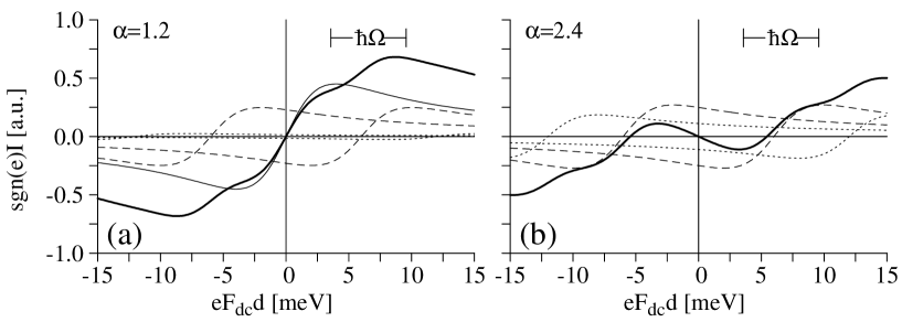
For small ac-fields we may set , while the higher order Bessel functions are approximately zero. Thus for and
| (200) | |||||
| (201) |
which can be viewed as a resistor and a capacitor in parallel yielding a complex admittance (small letters indicate quantities per period and the engineering convention is used here). Similar expressions were derived in Ref. [5] for the model with two scattering times. Both and may take positive or negative values. Furthermore note that is not the sample capacitance which has to be added in parallel as well, but originates from a quantum effect. (For small frequencies vanishes in the limit , if the functions and are kept constant.)
Eq. (200) shows that the derivative in the low-frequency response (189) is replaced by a finite difference on the quantum scale. A straightforward calculation for the Esaki-Tsu model gives for . In this range the superlattice structure can provide gain. Nevertheless one has to note, that this occurs in the range of negative differential conductivity, where the homogeneous field distribution is typically unstable as discussed in section 5.
In the limit of small scattering , the functions and vanish unless . From Eqs. (197,198,199) one finds for all components of the current vanish for . This can be interpreted as a dynamical localization [6] or the collapse of the miniband [7]: for a certain strength of the irradiation field the periodic structure does not conduct any current. In addition, a finite conductivity appears at opening up new transport channels, which are not present for in the limit of .
All these results have been obtained within the simple Esaki-Tsu model. Calculations within the energy balance model [238] provide similar results. If the dielectric relaxation is included, chaotic behavior [239] as well as a spontaneous generation of dc current [240] can be found. Recently, Monte-Carlo simulations of the Boltzmann equation under THz-irradiation have been performed, too [241].
6.3 Sequential tunneling
For sequential tunneling between two neighboring wells ( and ) Eqs. (197,198,199) hold again with the dc-expression from Eq. (79):
| (202) |
and the quantity
| (203) |
where equals in the limit of decoupled wells. (The definition used here differs by an -dependent shift of the energy scale from the one used in Sections 3.3 and B.1.) These expressions have been derived in [223] for a constant matrix elements . A similar derivation is provided in Appendix C. Furthermore it is shown there that Eq. (197) also applies to the case of a field-dependent matrix element , which is relevant for tunneling between nonequivalent levels. Note that the THz field also couples the different subbands via the term , which may cause further effects [242].
For sequential tunneling Eq. (197) has a simple interpretation. In the evaluation of the dc-current, gives the energy mismatch between the levels in well and . Under irradiation photons of energy can be absorbed or emitted during the tunneling process, which provides the energy mismatch for the absorption/emission of photons during the tunneling process. The Bessel functions represent the probability that an -photon process occurs assuming a classical radiation field (i.e. neglecting spontaneous emission). Eq. (197) then consists of the weighted sum of all possible photon-assisted tunneling processes. Similar results have been obtained in [243], where a strictly one-dimensional tight-binding lattice coupled to a heat bath has been considered (the approximation of incoherent tunneling dynamics applied there corresponds to sequential tunneling). An extended discussion of the methods used there can be found in [244].
As discussed in section 3 the structure of the first peak at low electric fields is similar for miniband transport and sequential tunneling. Therefore the discussion for miniband transport given in the preceding subsection holds for sequential tunneling as well. In addition, Eqs. (202,203) also describe the current peaks at resonances between different levels (a,b) in neighboring quantum wells. There one typically finds, see Eq. (83)
| (204) |
With the Kramers-Kronig relation one obtains
| (205) |
where the field dependence of has been neglected.
In the following some results are presented for the superlattice structure studied experimentally in [31, 120, 219] (15 nm wide GaAs wells, 5 nm Al0.3Ga0.7As barriers, doping density , cross section ). Results for this structure have been presented already in Fig. 12, where the complicated temperature dependence was discussed. Here we will focus to the behavior under irradiation. For these calculations a constant electron temperature K is assumed, which provides best agreement around the first maximum. Due to the presence of the irradiation field, it seems realistic that the electron gas does not even reach thermal equilibrium for vanishing dc-bias.
6.3.1 Rectified THz response
In Fig. 32 results are shown for the rectified current response under different strengths and frequencies of the irradiation field. Both from experiment and theory one observes a range of absolute negative conductance (i.e., for ) for low biases. Furthermore photon-assisted peaks are visible at field strengths . These findings are in qualitative agreement with the discussion of Fig. 31. Quantitative agreement between theory (Fig. 32a) and experiment (Fig. 32b) is found for meV (1.5 THz) for different strengths of the laser field. The low-field peak occurs at mV corresponding to direct tunneling. Photon replicas can be observed at mV and mV. For low bias and high intensities () there is a region of absolute negative conductance [31], which will be discussed in the following.
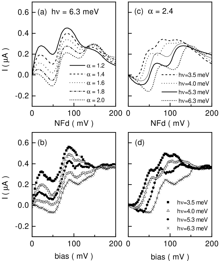
In Fig. 32d the laser intensity has been tuned such that maximal absolute negative conductance occurred for each of the different laser frequencies. Then one observes a minimum in the current at which is just the first photon replica of the direct tunneling peak on the negative bias side. This replica dominates the current if the direct tunneling channel is suppressed close to the zero of in Eq. (197), i.e., , as used in the calculation of Fig. 32c. Both the theoretical and experimental results show that absolute negative conductance persists in a wide range of frequencies but becomes less pronounced with decreasing photon energy. In the calculation absolute negative conductance vanishes for meV which is approximately equal to . (The latter relation has been verified by calculations for different samples as well.) For meV a smaller value of (thin line) agrees better with the experimental data (in the same sense the value agrees better for meV, compare Fig. 32a. This may be explained as follows: If strong NDC is present in doped superlattices, the homogeneous field distribution becomes unstable and either self-sustained oscillations or stable field domains form as discussed in section 5. Then the current-voltage characteristic deviates from the relation for homogeneous field distribution, where , and typically shows less pronounced NDC. Therefore maximal negative conductance is observed at a laser field corresponding to a value of , where the NDC is weaker and the field distribution is still homogeneous. The presence of an inhomogeneous field distribution could also explain the deviations between theory and experiment for mV. Quantitative agreement between theory and experiment regarding the rectified response was also obtained for a different superlattice structure, where up to seven photon replica of the first current peak could be observed [245].
6.3.2 Negative dynamical conductance
A semiconductor element is able to give gain at the given frequency if . In the low frequency limit (subsection 6.1) one obtains if is not too large. This means that gain is related to negative differential conductance in the static current-field relation . As such a situation is typically unstable with respect to the formation of inhomogeneous field distributions, it is difficult to apply this concept for a real device. Thus it would be of interest to have a system exhibiting in the THz frequency range considered but a positive differential conductance at . Inspection of Eq. (200) for the standard expressions (195,204) shows that is always positive as long as holds. Thus, it is a nontrivial task to find the opposite case in a semiconductor superlattice.
Fig. 33a shows the calculated current-field relation for the superlattice structure discussed here.

It exhibits a kind of plateau in the range 2 meV 9 meV, due to the presence of impurity bands which is observed experimentally as well (see Fig. 12). Experiments121212private communication from Stefan Zeuner show that this plateau is almost unchanged for lattice temperatures between 4 K and 35 K. At meV we have positive differential conductance, but the finite distance derivative for meV is clearly negative as indicated in the figure (see also [246]). Thus will be negative as long as is not too large and the terms with become important in Eq. (198). From Fig. 33b one obtains a negative dynamical conductance A/V at meV. Due to the higher order terms the dynamical conductance becomes positive for ac-field strengths larger than 8.5 mV per period. Fig. 33c,d show that negative dynamical conductance persists over a wide range of dc-bias and frequency. Nevertheless one must note that for meV the static conductance becomes negative yielding domain formation as observed experimentally (see Fig. 12).
Unfortunately, the negative dynamical conductance of the device considered here is compensated by the contact resistance. Measurements of the temperature dependent conductance of the sample yield values up to S (around K) at zero bias [120]. As a part of the resistance is from the superlattice itself one may conclude that the contact resistance is definitely smaller than 50 k in the sample. In comparison the dynamical resistance for 10 wells is k, which seems to dominate. But capacitive effects have to be taken into account: The sample capacitance per period is given by fF. This gives a total impedance
| (206) |
As ns, the negative dynamical resistance will be compensated even by a small contact resistance at THz frequencies. Thus, significant larger values of (i.e. higher current densities) are necessary for the observation of gain. Nevertheless, the effect discussed here is quite general and therefore gain should be observable in superlattice structures with special shapes for the dc-characteristic.
6.3.3 Tunneling capacitance
Now we want to investigate the reactive current from Eq. (199). As can be seen in Fig. 33d as well as in Fig. 34b) for low frequencies in the linear response region (i.e., small irradiation fields). This can be interpreted as a tunneling capacitance
| (207) |
as shown in Eq. (201).

In Fig. 34a the reactive current is displayed as a function of using a small irradiation field and a small frequency, so that Eq. (207) holds. The quantity shows a very characteristic behavior around the resonance with a minimum at meV, where the differential conductance is positive. This behavior can be understood within the approximation (205), yielding
| (208) |
which provides just the structure observed around meV. From Fig. 34b one obtains fF at meV, which is about 1.7% of the sample capacitance . It would be interesting if this tunneling capacitance can be measured. Here it may be useful to study superlattice structures with higher doping and larger coupling, which enhances the ratio between , as can be seen from Eq. (208).
6.3.4 Harmonic generation
In order to investigate harmonic generation the quantities have been plotted for in Fig. 35.

The basic frequency dominates for low irradiation fields, while the other quantities vanish like and as expected from the low-frequency limit (190). The current of the third harmonic is in the range of the dc-current at the first peak indicating strong harmonic generation. In the range meV the resonance becomes of importance which can be understood from the classical behavior . This provides a possibility to probe the second resonance even if it is not directly accessible due to sample heating. A similar idea to probe a peak by its response to an applied frequency has been performed in [247].
6.4 Discussion
In this chapter it has been shown that transport under irradiation is essentially governed by Eqs. (197,198,199). This scheme holds both for miniband transport within the relaxation time approximation and sequential tunneling for constant coupling matrix elements, albeit with different functions and . Therefore the question arises, if this structure might be general. Although this issue has not been settled finally, I believe that this is not the case. If one considers next-nearest neighbor tunneling processes within the model of sequential tunneling, it becomes obvious, that photon-assisted peaks occur at field strengths in contrast to the structure of Eq. (197). (This might provide an interesting tool to investigate tunneling processes where tunneling occurs between wells separated by more than one barrier [62, 127, 126].) The same behavior is found in a miniband model containing higher Fourier components in the band structure [248]. Therefore it seems that the structure of Eqs. (197,198,199) is limited to next-neighbor tunneling, or a cosine-shaped band structure , respectively. Further deviations may occur if the THz-field causes additional heating of the electron gas131313This was pointed out by A. A. Ignatov (private communication, 1998), which had been neglected in the models applied here.
The generic structure of the functions and is given by Eqs. (195,196,204,205). These imply the following typical effects under irradiation:
-
•
Photon-assisted peaks in the rectified current response at characteristic field strengths with integer values for next neighbor coupling.
-
•
Absolute negative conductance if the normalized ac-field strength is close the zeros of and .
-
•
Gain in most of the region of negative differential conductivity .
-
•
A quantum capacitance with the characteristic dependence (208) on the dc-field close to the resonances.
-
•
Generation of higher harmonics.
These effects rely on the structure of Eqs. (197,198,199) and should therefore (at least approximately) hold both for wide and narrow minibands. In addition, it has been shown that gain in the THz range is also possible in the region of positive differential conductance for appropriate shapes of the –relation.
7 Summary
In this review the transport properties of semiconductor superlattices have been analyzed. Strong emphasis has been given to the microscopic modeling of the stationary transport for a homogeneous electrical field as well as the formation of inhomogeneous field distributions leading to stationary field domains and self-sustained current oscillations.
The three different standard approaches, miniband transport, Wannier-Stark hopping, and sequential tunneling, have been reviewed in detail. Although the concepts applied are quite different, each approach provides negative differential conductivity for sufficiently high electric fields. While miniband transport and sequential tunneling provide an Ohmic behavior for low electric fields together with a maximum of the current around , Wannier-Stark hopping fails in the low-field region. In particular, good quantitative agreement with various transport measurements in weakly coupled superlattice structures has been obtained within the sequential tunneling model, both with and without irradiation.
The relation between the standard transport approaches could be identified by considering quantum transport based on nonequilibrium Green functions. It has been explicitly shown that the equations used for these simplified models can be obtained from the quantum transport model by applying various approximations. This justifies each of these approaches and sheds light on the respective ranges of applicability sketched in Fig. 7. Good quantitative agreement was found between self-consistent solutions of the quantum transport model with each of the simplified approaches in their respective ranges of applicability.
We have shown how different aspects of nonlinear pattern formation in semiconductor superlattices, such as the formation of stationary field domains as well as self-sustained oscillations, can be understood by the properties of traveling fronts. Fig. 27 shows that depletion and accumulation fronts travel with different velocities, which depend on the total current acting as a global coupling. This situation is similar to the Gunn diode albeit the discreteness of the superlattice structure allows for stationary fronts in a finite interval of current, when the front becomes trapped. As this trapping may occur in each of the wells, one obtains several branches (of the order of superlattice periods) in the global current voltage characteristics, which exhibits a typical sawtooth shape. The calculated current-voltage characteristics as well as the self-sustained oscillations are in reasonable quantitative agreement with experimental findings. Furthermore, the conditions for the occurrence of self-sustained oscillations have been discussed.
Under strong irradiation by a THz field, photon-assisted peaks appear, and absolute negative conductivity is possible. Both effects are predicted in a similar way by the sequential tunneling model and miniband transport. It has been demonstrated that there is a possibility for gain even in the region, where the low-frequency conductivity is positive (i.e. no field-domain formation effects are expected). In addition, the tunneling processes are connected with characteristic variations in the capacitance of the structure, which have not been observed so far.
8 Outlook
Even 30 years after the proposal by Esaki and Tsu, semiconductor superlattices continue to be a hot topic of ongoing research. Presently the following directions stand out:
- Superlattices with lower dimension:
-
In this work superlattice structures have been considered, where a free electron behavior is present in the two directions parallel to the layers. Presently, the first experiments have been performed where these lateral directions are confined. In Ref. [249] the measurement of the conduction through a stack of 50 InAs quantum dots was reported (see also [250]). Such structures can be regarded as a superlattice structure consisting of zero-dimensional boxes. Negative differential resistance was observed recently in a superlattice formed by quantum wires, fabricated by the method of cleaved edge overgrowth [251]. Due to the restricted phase space perpendicular to the transport direction, scattering should be strongly reduced in these structures, and strong effects related to the miniband structure are likely to be observed. Theoretical approaches to transport in such structures can be found in Refs. [252, 253] for quantum box superlattices and in Ref. [254] for a superlattice formed by quantum wires.
- Self-sustained current oscillations:
-
As discussed in section 5, traveling field domains cause self-generated current oscillations in superlattices. While the first experiments reported frequencies in the MHz range [19] at 5 K for a weakly coupled superlattice, frequencies up to 150 GHz at could be observed even at room temperature in specially designed superlattices with a large miniband width [20]. While it may be difficult to increase the fundamental frequency, the use of higher harmonics can be helpful for possible devices in the THz-range, although the prospects of this approach are under debate [255].
- Field domains in strongly coupled superlattices:
-
The formation of field domains is usually considered within the model of rate equation presented in Section 5.1. This model is justified for weakly coupled superlattices, where the electrons can be considered to be localized in single quantum wells. This localization becomes questionable for strongly coupled superlattices and it would be desireable to develop a quantum transport model, which takes into account both the inhomogeneity and the time dependence of the field distributions. (See also the discussion at the end of Section 5.)
- Chaos and nonlinear dynamics:
-
If the superlattice is driven by an ac-bias, chaotic behavior is likely to occur due to the presence of incommensurable frequencies, which is well known for the Gunn diode [256]. Simulations for semiconductor superlattices [257, 258] yield similar results. These chaotic oscillations could be observed experimentally [259, 260] and provide a nice example, where many aspects of chaotic systems [261] can be observed. There are also reports indicating undriven chaos under dc bias conditions in superlattices [259], which is not understood yet. In addition, frequency locking associated with the the occurrence of a Devil’s staircase has been observed [262]. These examples provide an interesting field to study general phenomena of nonlinear physics.
- Generation of THz signals:
-
Since the original proposal by Esaki and Tsu, it has been tempting to use the Bloch oscillator as a source for THz radiation. Unfortunately, only transient signals have been observed so far. Another possibility lies in the occurrence of a negative dynamical conductance. Here the problem arises that domain formation is a competing process in this region of parameter space. Two different scenarios have been proposed as a solution to this problem: In Ref. [246] it was proposed that for special shapes of the local current-field characteristic gain is possible even in the region where the low-frequency conductivity is positive, i.e., no field-domain formation effects are expected (see also section 6.3.2). A different possibility could be related to the fact that the low-frequency conductivity can become positive for large amplitudes of the ac fields [255], thus stabilizing the oscillation. It is not clear by now, if one of these effects may be useful to establish THz devices on the basis of semiconductor superlattices.
Appendix A Sequential tunneling with density matrices
As discussed in Section 3.3 the electrical transport in weakly coupled superlattices can be described by sequential tunneling. The idea of this concept is that the sates are essentially localized in single wells and the residual coupling causes transitions between neighboring wells. As this coupling ( for equivalent levels) is small, one can restrict the theory to the lowest order , which provides essentially Fermi’s golden rule. Already in Sec. 3.3 it was mentioned that scattering induced broadening is essential to recover the correct behavior for finite fields. This complication was treated within the theory of nonequilibrium Green functions which provided Eq. (79) as derived in Appendix B.1.
An alternative way to treat quantum transport is density matrix theory which also gives an exact treatment of both quantum effects and scattering. A recent overview can be found in [140]. Density matrix theory has been applied to superlattice transport in [73] for the evaluation of currents between nonequivalent levels. To my knowledge no such calculations exist regarding transport between equivalent levels with identical particle densities. In this case the calculation of [73] provides zero current independent of the electric field as shown below. A possible resolution of this problem will be presented in this appendix and a form similar to Eq. (83) will be derived. This demonstrates the equivalence of both approaches and highlights the differences in performance of both approaches.
A.1 The model
We use the Hamiltonian (23,24) in the basis of Wannier states and restrict ourselves to the lowest band for simplicity. Furthermore impurity and phonon scattering is taken into account within the restriction of intrawell scattering. Then the Hamiltonin reads with:
| (209) | |||||
| (210) | |||||
| (211) | |||||
| (212) |
In the following we assume that phonon scattering is strong enough to establish thermal equilibrium. Thus a thermal distribution function with chemical distribution can be assumed for each well. Furthermore, let us assume that impurity scattering is stronger than phonon scattering and dominates the broadening of the states, which simplifies the following calculations essentially. Correlations between the scattering matrix elements in different wells are neglected. (These drastic approximations make sense as we are mainly interested in the structure of the theory, not in quantitative results. The inclusion of different scattering mechanism should be possible in an analogous way.) In this case the self-energy within the Born approximation for impurity averaging is given by
| (213) |
where we neglected the real part and assumed that the scattering rate is energy independent for simplicity. Using Eq. (102) one obtains the current density from well to well
| (214) |
The task is the evaluation of the current in lowest order with respect to the coupling (sequential tunneling). Under these conditions the theory of nonequilibrium Green functions provides Eq. (79) which can be simplified to Eq. (83) for the self energy (213).
A.2 Density matrix theory
The key point is the temporal evaluation of . Similar to Eq. (101) the dynamics is given by
| (215) |
Here (and in the following) terms containing density matrices will be neglected as they provide terms of order in the current. As stationary states will be considered, the time dependence is dropped in most of the density matrices. On the right side new expressions of the type appear. Their temporal evolution is given by
| (216) |
and
| (217) |
These equations have again to be solved in the stationary state. In the following the key quantities of interest are the occupation of the mode in well and the corresponding polarizations which provide the current. They are given by
| (218) |
In the following, the more complicated density matrices appearing in Eqs. (216,217) have to be related to these quantities.
A.2.1 Lowest order calculation
In [73] only the lowest order terms within the impurity averaging process and the coupling have been considered for the evaluation of Eq. (215). As the current is already of order only terms up to or will be taken into account. Due to impurity averaging only the term remains then in Eq. (216) and we find in the stationary state
| (219) |
where the term ensures that the correlations vanish for . (An alternative way to obtain the factor is the application of the Markov limit, see [140].) Using the same argument we obtain from Eq. (217):
| (220) |
Inserting into Eq. (215) gives
| (221) |
where the approximation (213) has been used. This equation has also been applied in [263] to study time dependent phenomena. The stationary solution yields
| (222) |
and we obtain the current density via Eq. (214)
| (223) |
Taking into account that is the density of states, this expression is almost identical with Eq. (83). Nevertheless there is a significant difference: While in Eq. (83) the transport is driven by the difference of the occupation at the same energy, now the transport is driven by the difference of the occupation of the state in both wells. The latter difference becomes zero, if both wells have the same electron density. This has lead to the conclusion that no resonant tunneling peak occurs in weakly coupled superlattices for tunneling between equivalent levels [8], in contrast to the findings of section 3.3. Regarding tunneling between the ground state and excited states (which are typically empty) the respective formula provides a finite current which essentially agrees with the corresponding result of Eq. (83). The corresponding calculations have been presented in [73], where interwell correlations between scattering matrix elements were also taken into account.
A.2.2 Improved treatment
This problem can be circumvented by taking into account the last term in Eqs. (216,217) as well. Neglecting terms containing the coupling (which provide terms in the current) the dynamics of is given by:
| (224) |
By impurity averaging all terms vanish unless and or . Thus, we find in the stationary state:
| (225) |
Then the evaluation of Eq. (216) yields
| (226) |
and Eq. (217) gives
| (227) |
This provides further terms for Eq. (215), which becomes
| (228) |
Now we apply the relation and restrict ourselves to the imaginary parts. The isotropy in -space gives and we find with Eq. (213) the stationary solution
| (229) |
and the current (214) becomes
| (230) |
In contrast to Eq. (223) the current is now driven by the occupation difference taken at different values of so that the total energy is equal in both wells. This structure agrees with Eq. (83) and a finite current is found for identical occupation function . This shows that the terms , which had been neglected in the derivation of Eq. (223), are of crucial importance. They describe the internal correlations in the single quantum wells. These correlations correspond to the broadening of states in the Green function formalism, where they are taken into account by treating the probe energy and the energy of the bare state separately. As the broadening of the states is of crucial importance for the tunneling current, it becomes clear, that density matrix theory gives a wrong result if the corresponding matrices are neglected.
Appendix B Derivation of the standard approaches
In this appendix the relations between the quantum transport equations of section 4 and the standard approaches (miniband transport, Wannier-Stark hopping, and sequential tunneling as discussed in section 3) are examined. It will be shown, that the transport equations for the different standard approaches can be derived explicitly from the quantum transport model using various types of approximations. In each case the respective approximations can be justified within the range of validity of the given standard approach sketched in Fig. 7 and motivated in subsection 4.3.
B.1 Sequential tunneling
In the parameter ranges or the diagonal elements of dominate (see subsection 4.3) and an expansion of Eqs. (153,154) in is appropriate. In this way the formula for sequential tunneling (79) will be recovered as the leading order in of the general Eq. (148).
For we obtain which are determined by
| (231) |
and
| (232) |
where the self-energies are evaluated applying the Green-functions . These equations decouple in the well index. As no current flows in this case, one obtains the equilibrium solution
| (233) | |||||
| (234) |
with the spectral function
| (235) |
To first order in , Eq. (153) gives together with Eq. (231):
| (236) | |||||
| (237) | |||||
| (238) |
and Eq. (154) gives
| (239) |
Then the current is evaluated by Eq. (148)
| (240) |
which is just the expression (79) used for sequential tunneling.
B.2 Miniband conduction
If , the states in a semiconductor superlattice are essentially delocalized, as shown in subsection 4.3. In this case it makes sense to work in an extended basis like the Bloch states . The key point is the idea, that the occupation of these states can be treated as a semiclassical distribution function neglecting quantum mechanical correlations. We will show that the Boltzmann equation for as well as the formula for the current density (see Sec. 3.1) can be derived from the full quantum transport model under this assumption.
We consider a superlattice with a homogeneous electric field and a homogeneous carrier distribution. In this case it makes sense to use a local energy scale which refers to the bottom of the respective quantum well (here holds). We define
| (241) |
and is the same way. Now, only depends on the difference and due to the homogeneity of the system under stationary transport. Therefore it is helpful to define the spatial Fourier transform
| (242) |
This corresponds to the Fourier representation
| (243) |
which is the special case for a homogeneous electric field of the general gauge invariant version used in section 7 of [39] to obtain gauge invariant quantities [144]. The respective diagonal element of the density matrix is defined by
| (244) |
Applying Eq. (155) we obtain with these definitions
| (245) |
which is still exact. In the same way Eq. (153) yields:
| (246) |
Assuming that the self-energy does not depend strongly on 141414This implies that the density of final states for scattering processes does not vary strongly with energy. This variation occurs typically on the energy scale of the miniband width. Therefore this assumption can be justified for . within the energy scale , i.e. , this equation is solved by
| (247) |
On the energy scale the Green function essentially resembles the free particle Green function if and (so that the last term is negligible), which is just the condition (163).
Now we integrate both sides of Eq. (245) over energy , so that the terms on the right-hand side cancel each other. In the terms containing the self-energies the following approximations are performed:
-
•
The terms in energy dependence of the self-energies are neglected.
-
•
The expression is approximated by which holds exactly for the free particle Green functions.
-
•
We use . This means that the energetical width of the respective states is neglected. As information about quantum mechanical correlations is stored in the energy dependence (the Fourier transform of the time difference ), this approximation provides quasiclassical particles with specific momenta .
Then one finds
| (248) |
Now the same approximations are used in the evaluations of the self-energy for impurity scattering (150):
| (249) |
which is just (up to the factor ) the in-scattering term from Fermi’s golden rule. In the same way the term provides the out-scattering rate. It is instructive to note, that the insertion of Eqs. (151,152) gives the respective phonon scattering terms including the Pauli blocking factors . Thus, the Boltzmann equation can be derived as a limiting case of the full Kadanoff Baym equation if the scattering induced broadening as well as the field dependence is neglected in the scattering term. The same results essentially holds if the full space and time dependence is maintained, as shown in many textbooks, such as [39]. Some of these approximations can be relaxed. In particular, a significant improvement can be made by the generalized Kadanoff Baym ansatz [264, 265, 266, 267].
B.3 Wannier-Stark hopping
In subsection 4.3 it was shown that the Wannier-Stark states become resolved for . Here it will be shown that the equations (64,69) for the self-consistent Wannier-Stark hopping model can be derived from the of the quantum transport in this limit. Similar to the derivation of miniband transport, the key point is the idea, that the occupation of the Wannier-Stark states can be treated as a semiclassical distribution function neglecting quantum mechanical correlations. Similar derivations have been presented in [112, 252], where essentially the same approximations have been applied like in the quantum transport model discussed in this work.
According to Eq. (31) the Wannier-Stark states are with . The respective Green functions are given by
| (251) |
Within this new basis Eq. (153) becomes
| (252) |
with the definition
| (253) |
where the Born approximation was applied under the assumption, that scattering is diagonal in the Wannier basis, independent on the well number , and that no correlations exist between different wells . Furthermore we restrict ourselves to impurity scattering with matrix element for simplicity. In the same way Eq. (155) gives
| (254) |
The typical energy scale is given by . If the self-energies (of the order of ) are small in comparison to , Eq. (252) gives
| (255) |
describing free-particle Wannier-Stark states. The occupation of these states is governed by a semiclassical distribution yielding
| (256) |
Let us first consider the case , when the left-hand side of Eq. (254) vanishes. Applying the approximations (255,256) in the scattering term on the right-hand side and performing the integration we obtain
| (257) |
Inserting Eq. (253) one obtains together with the approximations (255,256):
| (258) |
where Eq. (67) has been inserted. This is just the condition for self-consistency (69) in the stationary case for the Wannier-Stark hopping approach.
The current is determined from Eq. (148) which can be rewritten as
| (259) |
(To verify this idendity insert all definitions into the second line and use for the homogeneous system) Now Eq. (254) can be inserted, where the approximations (255,256) are applied to the scattering terms. This yields:
| (260) |
where it has been used that is purely imaginary. Now we define the auxiliary function
| (261) |
which is an odd function of the difference for a homogeneous situation, when the occupation functions are independent from the index . Inserting Eq. (253) the first two summands of Eq. (260) yield:
| (262) |
where in the last line the relation and the symmetry for was applied. Comparing with the relation (67) one obtains:
| (263) |
which is just half the current density for Wannier-Stark hopping (64). Similarly the last two summands of Eq. (260) yield:
| (264) |
where in the second line , , and have been introduced. In the derivation of the last line, the term with prefactor vanishes by performing the sum. The final expression is identical to the second line of Eq. (262) and thus the full current density for Wannier-Stark hopping (64) is recovered from Eq. (260).
Appendix C Quantum transport under irradiation
In this appendix the quantum transport in superlattices under irradiation with a THz field is investigated. Together with a static field one obtains a potential with diagonal elements
| (265) |
in the Wannier basis, where is the ratio between the radiation field strength and its energy quantum. Similar to section 4 the theory of nonequilibrium Green functions is applied. The respective equations are derived in subsection C.1 for transport in the lowest miniband. In subsection C.2 it is shown that Eqs. (197-199) together with Eqs. (202,203) hold for sequential tunneling between equivalent levels , where the tunneling matrix element does not depend on the field. In contrast, the matrix element for the transition between different levels [see Eq. (24)] depends on time which provides further complications. This will be analyzed in subsection C.3, where it will be shown that Eq. (197) for the rectified response still holds in this case.
C.1 General formulation
In this subsection essentially the same approximation as in section 4.2 are applied. In particular the self-energies are assumed to be diagonal in the well index. For simplicity we set here. Neglecting scattering and coupling between the wells, the bare Green function reads
| (266) |
for the potential (265). Similar to [268] we define the on-site evolution
| (267) |
of the states and apply the following Fourier expansion for retarded functions
| (268) |
In particular this definition gives:
| (269) |
Now investigate
| (270) |
Similarly
| (271) |
With these relations Eq. (108) gives the recursion for the retarded Green function:
| (272) |
For the advanced functions we define
| (273) |
so that holds. The Fourier expansion of the lesser functions is defined by
| (274) |
Then we find the product
| (275) |
so that the Keldysh relation becomes
| (276) |
Eqs. (272,276) allow for a self-consistent solution provided the functionals for the self-energy are known. Within the self-consistent Born approximation they are given by the same functionals as in section 4.1.2 where the same index is added in the self-energies as well as the Green-functions. This diagonal structure in is due to the fact that the scattering matrix element is either not time dependent (for impurity scattering) or only depends on the time difference (for phonon scattering).
Finally, the current is given by
| (277) |
where has been used. Note that for homogeneous systems
| (278) |
holds which can simplify the calculation significantly.
C.2 Sequential tunneling
Now we want to derive the expression for sequential tunneling used in section 6.3. Like in Appendix B.1 the lowest order in the coupling yields a current . For vanishing coupling Eqs. (272,276) give and which are [up to the shift in the energy argument which eliminates the -dependence of ] the same functions as applied in Appendix B.1 without irradiation. Thus
| (279) |
In lowest order of the coupling one finds from Eq. (272):
| (280) | ||||
| (281) | ||||
| (282) | ||||
and in a similar way:
| (283) |
With these relations Eq. (276) gives
| (284) |
where was inserted in the last line. Inserting into Eq. (277) and sorting with respect to and we obtain Eqs. (197-199) with
| (285) |
and
| (286) |
This proves the formulas applied in section 6.3 for tunneling.
C.3 Tunneling between different levels
Now we want to consider tunneling between different levels. We will focus on the transitions from level in well to the level in well and omit the well indices in the following. According to Eq. (24), the matrix element for this transition becomes time dependent. Neglecting the coupling one obtains again the functions as in the preceding subsection. In the lowest order Eq. (108) yields
| (287) |
In the same way as Eq. (270) we obtain
| (288) |
Therefore we find
| (289) |
and the Keldysh relation becomes in analogy to the preceding subsection:
| (290) |
Finally, the current density can be obtained by inserting the time dependent matrix element into Eq. (277)
| (291) |
For , Eq. (197) can be recovered even in the case of a linear field dependence of the matrix element. In contrast, for Eqs. (198,199) only hold if the field dependence of the matrix element is negligible, which is appropriate if and hold.
References
- [1] F. Bloch, Über die Quantenmechanik der Elektronen in Kristallgittern, Z. Phys. 52 (1928) 555.
- [2] C. Zener, A theory of the electrical breakdown of solid dielectrics, Proc. Royal Soc. A 145 (1934) 523.
- [3] L. Esaki, R. Tsu, Superlattice and negative differential conductivity in semiconductors, IBM J. Res. Develop. 14 (1970) 61.
- [4] G. H. Wannier, Wave functions and effective Hamiltonian for Bloch electrons in an electric field, Phys. Rev. 117 (1960) 432.
- [5] S. A. Ktitorov, G. S. Simin, V. Y. Sindalovskii, Bragg reflections and the high-frequency conductivity of an electronic solid-state plasma, Sov. Phys.–Sol. State 13 (1972) 1872, [Fizika Tverdogo Tela 13, 2230 (1971)].
- [6] D. H. Dunlap, V. M. Kenkre, Dynamic localization of a charged particle under the influence of an electric field, Phys. Rev. B 34 (1986) 3625.
- [7] M. Holthaus, Collapse of minibands in far-infrared irradiated superlattices, Phys. Rev. Lett. 69 (1992) 351.
- [8] A. Y. Shik, Superlattices– periodic semiconductor structures, Sov. Phys. Semicond. 8 (1975) 1195, [Fiz. Tekh. Poluprov. 8, 1841 (1974)].
- [9] D. L. Smith, C. Mailhiot, Theory of semiconductor superlattice electronic structure, Rev. Mod. Phys. 62 (1990) 173.
- [10] E. L. Ivchenko, G. Pikus, Superlattices and other Heterostructures, Springer, Berlin, 1995.
- [11] M. Helm, Infrared spectroscopy and transport of electrons in semiconductor superlattices, Semicond. Sci. Technol. 10 (1995) 557.
- [12] H. T. Grahn (Ed.), Semiconductor Superlattices, Growth and Electronic Properties, World Scientific, Singapore, 1995.
- [13] F. Rossi, Bloch oscillations and Wannier-Stark localization in semiconductor superlattices, in: E. Schöll (Ed.), Theory of Transport Properties of Semiconductor Nanostructures, Chapman and Hall, London, 1998, Ch. 9.
- [14] F. G. Bass, A. P. Tetervov, High-frequency phenomena in semiconductor superlattices, Phys. Rep. 140 (1986) 237.
- [15] G. H. Döhler, n-i-p-i doping superlattice-semiconductors with tunable electronic properties, in: H. L. Grubin, K. Hess, G. J. Iafrate, D. K. Ferry (Eds.), The Physics of Submicron Structures, Plenum Press, New York, 1984.
- [16] L. Esaki, L. L. Chang, New transport phenomenon in a semiconductor superlattice, Phys. Rev. Lett. 33 (8) (1974) 495.
- [17] Y. Kawamura, K. Wakita, H. Asahi, K. Kurumada, Observation of room temperature current oscillation in InGaAs/InAlAs MQW pin diodes, Jpn. J. Appl. Phys. 25 (1986) L928.
- [18] M. Büttiker, H. Thomas, Current instability and domain propagation due to Bragg scattering, Phys. Rev. Lett. 38 (1977) 78.
- [19] J. Kastrup, R. Klann, H. T. Grahn, K. Ploog, L. L. Bonilla, J. Galán, M. Kindelan, M. Moscoso, R. Merlin, Self-oscillations of domains in doped GaAs-AlAs superlattices, Phys. Rev. B 52 (1995) 13761.
- [20] E. Schomburg, R. Scheurer, S. Brandl, K. F. Renk, D. G. Pavel’ev, Y. Koschurinov, V. Ustinov, A. Zhukov, A. Kovsh, P. S. Kop’ev, InGaAs/InAlAs superlattice oscillator at 147 GHz, Electronics Letters 35 (1999) 1491.
- [21] A. Sibille, J. F. Palmier, F. Mollot, H. Wang, J. C. Esnault, Negative differential conductance in GaAs/AlAs superlattices, Phys. Rev. B 39 (1989) 6272.
- [22] H. T. Grahn, K. von Klitzing, K. Ploog, G. H. Döhler, Electrical transport in narrow-miniband semiconductor superlattices, Phys. Rev. B 43 (1991) 12094.
- [23] E. Schomburg, A. A. Ignatov, S. Winnerl, J. Grenzer, K. F. Renk, D. G. Pavel’ev, Y. Koschurinov, B. Y. Melzer, V. Ustinov, S. Ivanov, S. S. ov, A. Zhukov, P. S. Kop’ev, Determination of the velocity-field characteristic of an esaki-tsu superlattice using an intense millimeter wave field, in: M. Scheffler, R. Zimmermann (Eds.), Proc. 23rd Int. Conf. Phys. Semicond., Berlin 1996, Vol. 3, World Scientific, Singapore, 1996, pp. 1679–1682.
- [24] E. E. Mendez, F. Agulló-Rueda, J. M. Hong, Stark localization in GaAs-GaAlAs superlattices under an electric field, Phys. Rev. Lett. 60 (1988) 2426.
- [25] P. Voisin, J. Bleuse, C. Bouche, S. Gaillard, C. Alibert, A. Regreny, Observation of the Wannier-Stark quantization in a semiconductor superlattice, Phys. Rev. Lett. 61 (1988) 1639.
- [26] K. H. Schmidt, N. Linder, G. H. Döhler, H. T. Grahn, K. Ploog, H. Schneider, Coexistence of Wannier-Stark transitions and miniband Franz-Keldysh oscillations in strongly coupled GaAs-AlAs superlattices, Phys. Rev. Lett. 72 (1994) 2769.
- [27] N. Ohtani, C. Domoto, N. Egami, H. Mimura, M. Ando, M. Nakayama, M. Hosoda, Electric-field-induced combination of Wannier-Stark localization and type-I–type-II crossover in a marginal type-I GaAs/AlAs superlattice, Phys. Rev. B 61 (2000) 7505.
- [28] J. Feldmann, K. Leo, J. Shah, D. A. B. Miller, J. E. Cunningham, T. Meier, G. von Plessen, A. Schulze, P. Thomas, S. Schmitt-Rink, Optical investigation of Bloch oscillations in a semiconductor superlattice, Phys. Rev. B 46 (1992) 7252.
- [29] C. Waschke, H. G. Roskos, K. Schwedler, K. Leo, H. Kurz, K. Köhler, Coherent submillimeter-wave emission from Bloch oscillations in a semiconductor superlattice, Phys. Rev. Lett. 70 (1993) 3319.
- [30] V. G. Lyssenko, G. Valušis, F. Löser, T. Hasche, K. Leo, M. M. Dignam, K. Köhler, Direct measurement of the spatial displacement of Bloch-oscillating electrons in semiconductor superlattices, Phys. Rev. Lett. 79 (1997) 301.
- [31] B. J. Keay, S. Zeuner, S. J. Allen, K. D. Maranowski, A. C. Gossard, U. Bhattacharya, M. J. M. Rodwell, Dynamic localization, absolute negative conductance, and stimulated, multiphoton emission in sequential resonant tunneling semiconductor superlattices, Phys. Rev. Lett. 75 (1995) 4102.
- [32] S. Winnerl, S. Seiwerth, E. Schomburg, J. Grenzer, K. F. Renk, C. J. G. M. Langerak, A. F. G. van der Meer, D. G. Pavel’ev, Y. Koschurinov, A. A. Ignatov, B. Melzer, V. Ustinov, S. Ivanov, P. S. Kop’ev, Ultrafast detection and autocorrelation of picosecond THz radiation pulses with a GaAs/AlAs superlattice, Appl. Phys. Lett. 73 (1998) 2983.
- [33] R. Tsu, G. Döhler, Hopping conduction in a superlattice, Phys. Rev. B 12 (1975) 680.
- [34] D. Miller, B. Laikhtman, Theory of high-field-domain structures in superlattices, Phys. Rev. B 50 (1994) 18426.
- [35] A. Wacker, Vertical transport and domain formation in multiple quantum wells, in: E. Schöll (Ed.), Theory of Transport Properties of Semiconductor Nanostructures, Chapman and Hall, London, 1998, Ch. 10.
- [36] A. Wacker, A.-P. Jauho, Quantum transport: The link between standard approaches in superlattices, Phys. Rev. Lett. 80 (1998) 369.
- [37] R. Kubo, Statistical-mechanical theory of irreversible processes I, J. Phys. Soc. Japan 12 (1957) 570.
- [38] S. Datta, Electronic Transport in Mesoscopic Systems, Cambridge University Press, Cambridge, 1995.
- [39] H. Haug, A.-P. Jauho, Quantum Kinetics in Transport and Optics of Semiconductors, Springer, Berlin, 1996.
- [40] D. K. Ferry, S. M. Goodnick, Transport in Nanostructures, Cambridge University Press, Cambridge, 1997.
- [41] E. Schöll (Ed.), Theory of Transport Properties of Semiconductor Nanostructures, Vol. 4 of Electronic Materials Series, Chapman and Hall, London, 1998.
- [42] T. Dittrich, P. Hänggi, G.-L. Ingold, B. Kramer, G. Schön, W. Zwerger, Quantum Transport and Dissipation, Wiley-VCH, Weinheim, 1998.
- [43] E. Schöll, Nonequilibrium Phase Transitions in Semiconductors, Springer, Berlin, 1987.
- [44] Y. Abe (Ed.), Nonlinear and Chaotic Transport Phenomena in Semiconductors, Special issue of Applied Phys. A 48, pp. 93-191, 1989.
- [45] M. P. Shaw, V. V. Mitin, E. Schöll, H. L. Grubin, The Physics of Instabilities in Solid State Electron Devices, Plenum Press, New York, 1992.
- [46] F.-J. Niedernostheide (Ed.), Nonlinear Dynamics and Pattern Formation in Semiconductors and Devices, Springer, Berlin, 1995.
- [47] E. Schöll, Nonlinear spatio-temporal dynamics and chaos in semiconductors, Cambridge University Press, Cambridge, 2001.
- [48] L. L. Chang, L. Esaki, R. Tsu, Resonant tunneling in semiconductor double barriers, Appl. Phys. Lett. 24 (1974) 593.
- [49] J. Faist, F. Capasso, D. L. Sivco, C. Sirtori, A. L. Hutchinson, A. Y. Cho, Quantum cascade laser, Science 264 (1994) 553.
- [50] Y. Ando, T. Itoh, Calculation of transmission tunneling current across arbitrary potential barriers, J. Appl. Phys. 61 (1987) 1497.
- [51] P. Y. Yu, M. Cardona, Fundamentals of Semiconductors, 2nd Edition, Springer, Berlin, 1999.
- [52] D. J. BenDaniel, C. B. Duke, Space-charge effects on electron tunneling, Phys. Rev. 152 (1966) 683.
- [53] G. Bastard, Wave Mechanics Applied to Semiconductor Heterostructures, Les Editions de Physique, Les Ulis Cedex, France, 1988.
- [54] S. Adachi (Ed.), Properties of Aluminium Gallium Arsenide, INSPEC, London, 1993.
- [55] S. R. White, L. J. Sham, Electronic properties of flat-band semiconductor heterostructures, Phys. Rev. Lett. 47 (1981) 879.
- [56] G. Brozak, E. A. de Andrada e Silva, L. J. Sham, F. DeRosa, P. Miceli, S. A. Schwarz, J. P. Harbison, L. T. Florez, S. J. Allen, Tunneling cyclotron resonance and the renormalized effective mass in semiconductor barriers, Phys. Rev. Lett. 64 (1990) 471.
- [57] M. Hosoda, N. Ohtani, H. Mimura, K. Tominaga, T. Watanabe, H. Inomata, K. Fujiwara, Carrier transport affected by transfer in GaAs/AlAs superlattices, Phys. Rev. B 58 (1998) 7166.
- [58] J. A. Støvneng, P. Lipavský, Multiband tight-binding-approach to tunneling in semiconductor heterostructures: Application to X transfer in GaAs, Phys. Rev. B 49 (1994) 16494.
- [59] D. Z. Ting, T. C. McGill, Multiband and multidimensional analysis of quantum transport in ultrasubmicron devices, in: D. K. Ferry, H. L. Grubin, C. Jacoboni, A.-P. Jauho (Eds.), Quantum Transport in Ultrasmall Devices, Plenum Press, New York, 1995, p. 417.
- [60] M. Ogawa, T. Sugano, R. Tominaga, T. Miyoshi, Multi-band simulation of resonant tunneling diodes with scattering effects, Physica B 272 (1999) 167.
- [61] R. d. L. Kronig, W. G. Penney, Quantum mechanics of electrons in crystal lattices, Proc. Royal Soc. A 130 (1931) 499.
- [62] A. Kristensen, P. E. Lindelof, C. B. Sørensen, A. Wacker, Resonant tunnelling in superlattices with a basis, Semicond. Sci. Technol. 13 (1998) 910.
- [63] L. Wang, S. Wey, T. Mattila, A. Zunger, I. Vurgaftman, J. R. Meyer, Multiband coupling and electronic structure of (InAs)n/(GaSb)n superlattices, Phys. Rev. B 60 (1999) 5590.
- [64] C. Rauch, G. Strasser, K. Unterrainer, W. Boxleitner, E. Gornik, A. Wacker, Transition between coherent and incoherent electron transport in GaAs/GaAlAs superlattices, Phys. Rev. Lett. 81 (1998) 3495.
- [65] G. D. Mahan, Many-Particle Physics, Plenum, New York, 1990.
- [66] F. Prengel, A. Wacker, E. Schöll, Simple model for multistability and domain formation in semiconductor superlattices, Phys. Rev. B 50 (1994) 1705, ibid 52, 11518 (1995).
- [67] R. Aguado, G. Platero, M. Moscoso, L. L. Bonilla, Microscopic model for sequential tunneling in semiconductor multiple quantum wells, Phys. Rev. B 55 (1997) 16053.
- [68] J. Bardeen, Tunnelling from a many-particle point of view, Phys. Rev. Lett. 6 (1961) 57.
- [69] G. H. Wannier, The structure of electronic excitation levels in insulating crystals, Phys. Rev. 52 (1937) 191.
- [70] W. Kohn, Analytic properties of Bloch waves and Wannier functions, Phys. Rev. 115 (1959) 809.
- [71] F. B. Pedersen, G. T. Einevoll, P. C. Hemmer, Wannier functions for the Kronig-Penney model, Phys. Rev. B 44 (1991) 5470.
- [72] M. Abramowitz, I. A. Stegun, Handbook of Mathematical Functions, National Bureau of Standards, Washington, D.C., 1966.
- [73] R. F. Kazarinov, R. A. Suris, Electric and electromagnetic properties of semiconductors with a superlattice, Sov. Phys. Semicond. 6 (1) (1972) 120, [Fiz. Tekh. Poluprov. 6, 148 (1972)].
- [74] G. S. Vieira, S. J. Allen, P. S. S. Guimaraes, K. L. Campman, A. C. Gossard, Resonantly enhanced photon-assisted tunneling in a multiple-quantum-well superlattice, Phys. Rev. B 58 (1998) 7136.
- [75] J. Zak, Stark ladders in solids?, Phys. Rev. Lett. 20 (1968) 1477.
- [76] G. Nenciu, Dynamics of band electrons in electric and magnetic fields: rigorous justification of the effective Hamiltonians, Rev. Mod. Phys. 63 (1991) 91.
- [77] F. Agulló-Rueda, J. Feldmann, Wannier-Stark localization and Bloch oscillations, in: H. T. Grahn (Ed.), Semiconductor Superlattices, Growth and Electronic Properties, World Scientific, Singapore, 1995, Ch. 3.
- [78] E. O. Kane, Zener tunneling in semiconductors, J. Phys. Chem. Solids 12 (1959) 181.
- [79] M. C. Chang, Q. Niu, Local density of states and level width for Wannier-Stark ladders, Phys. Rev. B 48 (1993) 2215.
- [80] H. Fukuyama, R. A. Bari, H. C. Fogedby, Tightly bound electrons in a uniform electric field, Phys. Rev. B 8 (1973) 5579.
- [81] I. S. Gradshteyn, I. M. Ryzhik, Table of Integrals, Series, and Products, Academic Press, New York, 1980.
- [82] A. M. Bouchard, M. Luban, Bloch oscillations and other dynamical phenomena of electrons in superlattices, Phys. Rev. B 52 (1995) 5105.
- [83] A. Sibille, J. F. Palmier, H. Wang, F. Mollot, Observation of Esaki-Tsu negative differential velocity in GaAs/AlAs superlattices, Phys. Rev. Lett. 64 (1990) 52.
- [84] J. F. Palmier, A. Sibille, G. Etemadi, A. Celeste, J. C. Portal, Non-linear miniband conduction in crossed electric and magnetic fields, Sol. Stat. Comm. 7 (1992) B283.
- [85] D. Miller, B. Laikhtman, Semiclassical theory of the perpendicular magnetoresistance in superlattices, Phys. Rev. B 52 (1995) 12191.
- [86] H. J. Hutchinson, A. W. Higgs, D. C. Herbert, G. W. Smith, Observation of miniband transport in GaAs/Al0.33Ga0.67As superlattices, J. Appl. Phys. 75 (1994) 320.
- [87] E. H. Cannon, F. V. Kusmartsev, K. N. Alekseev, D. K. Campbell, Absolute negative conductivity and spontaneous current generation in semiconductor superlattices with hot electrons, Phys. Rev. Lett. 85 (2000) 1302.
- [88] D. Ferry, Semiconductors, Macmillan Publishing Company, New York, 1991.
- [89] K. Seeger, Semiconductor Physics, 6th Edition, Springer, 1996.
- [90] I. Dharssi, P. N. Butcher, Interface roughness scattering in a superlattice, J. Phys.: Condens. Matter 2 (1990) 4629.
- [91] G. Etemadi, J. F. Palmier, Effect of interface roughness on non-linear vertical transport in GaAs/AlAs superlattices, Sol. Stat. Comm. 86 (1993) 739.
- [92] S. Rott, Theory of electronic transport in semiconductor superlattices, Ph.D. thesis, Universität Erlangen, vol. 8 of Physik Mikrostrukturierter Halbleiter, edited by T. Marek, S. Malzer, and P.Kiesel, ISBN 3-932392-16-7 (Lehrstuhl für Mikrocharakterisierung, Erlangen, 1999) (1999).
- [93] A. Sibille, Miniband transport, in: H. T. Grahn (Ed.), Semiconductor Superlattices, Growth and Electronic Properties, World Scientific, Singapore, 1995, Ch. 2.
- [94] C. Jacoboni, L. Reggiani, The Monte Carlo method for the solution of charge transport in semiconductors with application to covalent materials, Rev. Mod. Phys. 55 (1983) 645.
- [95] C. Jacoboni, R. Brunetti, P. Bordone, Monte Carlo simulation of semiconductor transport, in: E. Schöll (Ed.), Theory of Transport Properties of Semiconductor Nanostructures, Chapman and Hall, London, 1998, Ch. 3.
- [96] P. A. Lebwohl, R. Tsu, Electrical transport properties in a superlattice, J. Appl. Phys. 41 (1970) 2664.
- [97] Y. A. Pusep, A. J. Chiquito, S. Mergulhão, J. C. Galzerani, One-dimensional character of miniband transport in doped GaAs/AlAs superlattices, Phys. Rev. B 56 (1997) 3892.
- [98] G. Brozak, M. Helm, F. DeRosa, C. H. Perry, M. Koza, R. Bhat, S. J. Allen, Thermal saturation of band transport in a superlattice, Phys. Rev. Lett. 64 (1990) 3163.
- [99] A. Sibille, J. F. Palmier, M. Hadjazi, H. Wang, G. Etemadi, E. Dutisseuil, F. Mollot, Limits of semiclassical transport in narrow miniband GaAs/AlAs superlattices, Superlattices and Microstructures 13 (1993) 247.
- [100] A. A. Ignatov, E. P. Dodin, V. I. Shashkin, Transient response theory of semiconductor superlattices: Connection with Bloch oscillations, Mod. Phys. Lett. B 5 (1991) 1087.
- [101] E. Schomburg, T. Blomeier, K. Hofbeck, J. Grenzer, S. Brandl, I. Lingott, A. A. Ignatov, K. F. Renk, D. G. Pavel’ev, Y. Koschurinov, B. Y. Melzer, V. Ustinov, S. Ivanov, A. Zhukov, P. S. Kop’ev, Current oscillation in superlattices with different miniband widths, Phys. Rev. B 58 (1998) 4035.
- [102] S. Rott, P. Binder, N. Linder, G. H. Döhler, Combined description for semiclassical and quantum transport in superlattices, Phys. Rev. B 59 (1999) 7334.
- [103] H. Krömer, Zur Theorie des Germaniumgleichrichters und des Transistors, Z. Phys. 134 (1953) 435.
- [104] R. R. Gerhardts, Effect of elastic scattering on miniband transport in semiconductor superlattices, Phys. Rev. B 48 (1993) 9178.
- [105] X. L. Lei, N. J. M. Horing, H. L. Cui, Theory of negative differential conductivity in a superlattice miniband, Phys. Rev. Lett. 66 (1991) 3277.
- [106] M. Rudan, M. Lorenzini, R. Brunetti, Hydrodynamic simulation of semiconductor devices, in: E. Schöll (Ed.), Theory of Transport Properties of Semiconductor Nanostructures, Chapman and Hall, London, 1998, Ch. 2.
- [107] D. L. Andersen, E. J. Aas, Monte Carlo calculation of the electron drift velocity in GaAs with a superlattice, J. Appl. Phys. 44 (1973) 3721.
- [108] P. J. Price, Transport properties of the semiconductor superlattice, IBM J. Res. Develop. 17 (1973) 39.
- [109] M. Artaki, K. Hess, Monte Carlo calculations of electron transport in GaAs/AlGaAs superlattices, Superlattices and Microstructures 1 (1985) 489.
- [110] S. Rott, P. Binder, N. Linder, G. H. Döhler, A combined model for miniband and hopping transport in superlattices, Physica E 2 (1998) 511.
- [111] M. Morifuji, C. Hamaguchi, Stark-ladder states in an imperfect crystal: Effect of impurity scattering, Phys. Rev. B 58 (1998) 12842.
- [112] D. Calecki, J. F. Palmier, A. Chomette, Hopping conduction in multiquantum well structures, J. Phys. C: Solid State Phys. 17 (1984) 5017.
- [113] S. Rott, N. Linder, G. H. Döhler, Hopping transport in superlattices, Superlattices and Microstructures 21 (1997) 569.
- [114] F. Capasso, K. Mohammed, A. Y. Cho, Sequential resonant tunneling through a multiquantum well superlattice, Appl. Phys. Lett. 48 (1986) 478.
- [115] L. Canali, M. Lazzarino, L. Sorba, F. Beltram, Stark-cyclotron resonance in a semiconductor superlattice, Phys. Rev. Lett. 76 (1996) 3618.
- [116] R. D. Mattuck, A Guide to Feynman Diagrams in the Many Body Problem, Republication by Dover, New York, 1992.
- [117] S. Q. Murphy, J. P. Eisenstein, L. N. Pfeiffer, K. W. West, Lifetime of two-dimensional electrons measured by tunneling spectroscopy, Phys. Rev. B 52 (1995) 14825.
- [118] N. Turner, J. T. Nicholls, E. H. Linfield, K. M. Brown, G. A. C. Jones, D. A. Ritchie, Tunneling between parallel two-dimensional electron gases, Phys. Rev. B 54 (1996) 10614.
- [119] L. Zheng, A. H. MacDonald, Tunneling conductance between parallel two-dimensional electron systems, Phys. Rev. B 47 (1993) 10619.
- [120] A. Wacker, A.-P. Jauho, S. Zeuner, S. J. Allen, Sequential tunneling in doped superlattices: Fingerprints of impurity bands and photon-assisted tunneling, Phys. Rev. B 56 (1997) 13268.
- [121] J. Serre, A. Ghazali, A. Gold, Impurity levels, impurity bands, exited impurity bands, and band tails: The electronic density of states in quantum wells and heterostructures, Phys. Rev. B 39 (1989) 8499.
- [122] A. Wacker, A.-P. Jauho, Microscopic modelling of perpendicular electronic transport in doped multiple quantum wells, Physica Scripta T69 (1997) 321.
- [123] H. T. Grahn, R. J. Haug, W. Müller, K. Ploog, Electric-field domains in semiconductor superlattices: A novel system for tunneling between 2D systems, Phys. Rev. Lett. 67 (1991) 1618.
- [124] S. H. Kwok, H. T. Grahn, M. Ramsteiner, K. Ploog, F. Prengel, A. Wacker, E. Schöll, S. Murugkar, R. Merlin, Non-resonant carrier transport through high-field domains in semiconductor superlattices, Phys. Rev. B 51 (1995) 9943.
- [125] V. N. Murzin, Y. A. Mityagin, V. A. Chuenkov, A. L. Karuzskii, A. V. Perestoronin, L. Y. Shchurova, Resonant tunneling and intersubband population inversion effects in asymmetric wide quantum well structures, Physica E 7 (2000) 58.
- [126] M. Helm, W. Hilber, G. Strasser, R. D. Meester, F. M. Peeters, A. Wacker, Continuum Wannier-Stark ladders strongly coupled by Zener resonances in semiconductor superlattices, Phys. Rev. Lett. 82 (1999) 3120.
- [127] A. Sibille, J. F. Palmier, F. Laruelle, Zener interminiband resonant breakdown in superlattices, Phys. Rev. Lett. 80 (1998) 4506.
- [128] X.-G. Zhao, D. W. Hone, Zener transitions between dissipative Bloch bands. II current response at finite temperature, Phys. Rev. B 62 (2000) 5010.
- [129] A. Di Carlo, P. Vogl, W. Pötz, Theory of Zener tunneling and Wannier-Stark states in semiconductors, Phys. Rev. B 50 (1994) 8358.
- [130] R. Lake, G. Klimeck, R. C. Bowen, D. Jovanovic, Single and multiband modeling of quantum electron transport through layered semiconductor devices, J. Appl. Phys. 81 (1997) 7845.
- [131] F. Rossi, A. Di Carlo, P. Lugli, Microscopic theory of quantum-transport phenomena in mesoscopic systems: A Monte Carlo approach, Phys. Rev. Lett. 80 (1998) 3348.
- [132] M. V. Fischetti, Master-equation approach to the study of electronic transport in small semiconductor devices, Phys. Rev. B 59 (1999) 4901.
- [133] P. Bordone, M. Pascoli, R. Brunetti, A. Bertoni, C. Jacoboni, A. Abramo, Quantum transport of electrons in open nanostructures with the Wigner-function formalism, Phys. Rev. B 59 (1999) 3060.
- [134] R. A. Suris, B. S. Shchamkhalova, Heating of electrons in superlattice semicondctors, Sov. Phys. Semicond. 18 (1984) 738, [Fiz. Tekh. Poluprovodn. 18, 1178 (1984)].
- [135] R. A. Suris, B. S. Shchamkhalova, Conductivity of a semicondctor superlattice in a magnetic field perpendicular to its axis, Sov. Phys. Semicond. 24 (1990) 1023, [Fiz. Tekh. Poluprovodn. 24, 1638 (1990)].
- [136] V. V. Bryksin, P. Kleinert, Microscopic theory of high-field transport in semiconductor superlattices, J. Phys.: Condens. Matter 9 (1997) 7403.
- [137] P. Kleinert, V. V. Bryksin, High-field miniband transport in semiconductor superlattices in parallel electric and magnetic fields, Phys. Rev. B 56 (1997) 15827.
- [138] B. Laikhtman, D. Miller, Theory of current-voltage instabilities in superlattices, Phys. Rev. B 48 (1993) 5395.
- [139] H. Haug, S. Koch, Quantum theory of the optical and electronic properties of semiconductors, World Scientific, Singapore, 1994.
- [140] T. Kuhn, Density matrix theory of coherent ultrafast dynamics, in: E. Schöll (Ed.), Theory of Transport Properties of Semiconductor Nanostructures, Chapman and Hall, London, 1998.
- [141] L. P. Kadanoff, G. Baym, Quantum Statistical Mechanics, Benjamin, New York, 1962.
- [142] L. V. Keldysh, Diagram technique for nonequilibrium processes, Sov. Phys. JETP 20 (1965) 1018, [Zh. Eksp. Theor. Fiz. 47, 1515 (1964)].
- [143] D. C. Langreth, Linear and nonlinear response theory with application, in: J. T. Devreese, V. E. van Doren (Eds.), Linear and Nonlinear Electron Transport in Solids, Plenum Press, New York, 1976.
- [144] R. Bertoncini, A.-P. Jauho, Gauge-invariant formulation of the intracollisional field effect including collisional broadening, Phys. Rev. B 44 (1991) 3655.
- [145] A. Wacker, B. Y.-K. Hu, Theory of transmission through disorderd superlattices, Phys. Rev. B 60 (1999) 16039.
- [146] Y. Meir, N. S. Wingreen, Landauer formula for the current through an interacting electron region, Phys. Rev. Lett. 68 (1992) 2512.
- [147] M. Büttiker, Four-terminal phase-coherent conductance, Phys. Rev. Lett. 57 (1986) 1761.
- [148] S. Datta, A simple kinetic equation for steady-state quantum transport, J. Phys.: Condens. Matter 2 (1990) 8023.
- [149] A.-P. Jauho, N. S. Wingreen, Y. Meir, Time-dependent transport in interacting and noninteracting resonant-tunneling systems, Phys. Rev. B 50 (1994) 5528.
- [150] V. Holý, T. Baumbach, Nonspecular x-ray reflection from rough multilayers, Phys. Rev. B 49 (1994) 10668.
- [151] J. Menniger, H. Kostial, U. Jahn, R. Hey, H. T. Grahn, Depth correlated lateral variations of layer thicknesses in GaAs-AlGaAs multiple quantum wells investigated by cathodoluminescence, Appl. Phys. Lett. 66 (1995) 2349.
- [152] W. Szott, C. Jedrzejek, W. P. Kirk, Structure-dependent weak-localization model for a superlattice, Phys. Rev. B 45 (1992) 3565.
- [153] W. Szott, C. Jedrzejek, W. P. Kirk, Influence of bandwidth and dopant profile on quantum interference from superlattice transport studies, Phys. Rev. B 48 (1993) 8963.
- [154] E. Schomburg, S. Brandl, K. Hofbeck, T. Blomeier, J. Grenzer, A. A. Ignatov, K. F. Renk, D. G. Pavel’ev, Y. Koschurinov, V. Ustinov, A. Zhukov, A. Kovsch, S. Ivanov, P. S. Kopev, Generation of millimeter waves with a GaAs/AlAs superlattice oscillator, Appl. Phys. Lett. 72 (1998) 1498.
- [155] A. Wacker, A.-P. Jauho, S. Rott, A. Markus, P. Binder, G. H. Döhler, Inelastic quantum transport in superlattices: Success and failure of the Boltzmann equation, Phys. Rev. Lett. 83 (1999) 836.
- [156] L. Reggiani, P. Lugli, A.-P. Jauho, Quantum kinetic equation for electronic transport in nondegenerate semiconductors, Phys. Rev. B 36 (1987) 6602.
- [157] L. Reggiani, L. Rota, L. Varani, Spectral functions and collisional broadening in semiconductor ultra-high field transport, phys. status solidi (b) 204 (1997) 306.
- [158] H. Steuer, Selbstgenerierte Oszillationen in Halbleiterübergittern, Master’s thesis, TU Berlin (1999).
- [159] H. Steuer, A. Wacker, E. Schöll, Complex behavior due to electron heating in superlattices exhibiting high-frequency current oscillations, Physica B 272 (1999) 202.
- [160] J. B. Gunn, Instabilities of current in III-V semiconductors, IBM J. Res. Develop. 8 (1964) 141.
- [161] H. Kroemer, Theory of the Gunn effect, Proc. IEEE 52 (1964) 1736.
- [162] D. E. McCumber, A. G. Chynoweth, Theory of negative-conductance amplification and of Gunn instabilities in two-valley semiconductors, IEEE electron devices 13 (1966) 4.
- [163] B. W. Knight, G. A. Peterson, Theory of the Gunn effect, Phys. Rev. 155 (1967) 393.
- [164] K. W. Böer, G. Döhler, Influence of boundary conditions on high-field domains in Gunn diodes, Phys. Rev. 186 (1969) 793.
- [165] F. J. Higuera, L. L. Bonilla, Gunn instability in finite samples of GaAs – II. Oscillatory states in long samples, Physica D 57 (1992) 161.
- [166] L. L. Bonilla, I. R. Cantalapiedra, G. Gomila, J. M. Rubí, Asymptotic analysis of the Gunn effect with realistic boundary conditions, Phys. Rev. E 56 (1997) 1500.
- [167] M. Büttiker, H. Thomas, Bifurcation and stability of dynamical structures at a current instability, Z. Phys. B 34 (1979) 301.
- [168] K. Hofbeck, J. Grenzer, E. Schomburg, A. A. Ignatov, K. F. Renk, D. G. Pavel’ev, Y. Koschurinov, B. Melzer, S. Ivanov, S. Schaposchnikov, P. S. Kop’ev, High-frequency self-sustained current oscillation in an Esaki-Tsu superlattice monitored via microwave emission, Phys. Lett. A 218 (1996) 349.
- [169] E. Schomburg, M. Henini, J. M. Chamberlain, D. P. Steenson, S. Brandl, K. Hofbeck, K. F. Renk, W. Wegscheider, Self-sustained current oscillation above 100 GHz in a GaAs/AlAs superlattice, Appl. Phys. Lett. 74 (1999) 2179.
- [170] K. K. Choi, B. F. Levine, R. J. Malik, J. Walker, C. G. Bethea, Periodic negative conductance by sequential resonant tunneling through an expanding high-field superlattice domain, Phys. Rev. B 35 (1987) 4172.
- [171] M. Helm, P. England, E. Colas, F. DeRosa, S. J. Allen, Jr., Intersubband emission from semiconductor superlattices excited by sequential resonant tunneling, Phys. Rev. Lett. 63 (1989) 74.
- [172] P. Helgesen, T. G. Finstad, Sequential resonant and non-resonant tunneling in GaAs/AlGaAs multiple quantum well structures: High field domain formation, in: O. Hansen (Ed.), Proceedings of the Nordic Semiconductor Meeting, University of Århus, Århus, 1990, p. 323.
- [173] Z. Y. Han, S. F. Yoon, K. Radhakrishnan, D. H. Zhang, Space charge buildup in tight-binding superlattices induced by electron sequential tunneling, Superlattices and Microstructures 18 (1995) 83.
- [174] Y. A. Mityagin, V. N. Murzin, Y. A. Efimov, G. K. Rasulova, Sequential excited-to-excited states resonant tunneling and electric field domains in long period superlattices, Appl. Phys. Lett. 70 (1997) 3008.
- [175] Y. Shimada, K. Hirakawa, Sequential resonant magnetotunneling through Landau levels in GaAs/AlGaAs multiple quantum well structures, phys. status solidi (b) 204 (1997) 427.
- [176] T. Schmidt, A. G. M. Jansen, R. J. Haug, K. von Klitzing, K. Eberl, Magnetic control of electric-field domains in semiconductor superlattices, Phys. Rev. Lett. 81 (1998) 3928.
- [177] Y. Shimada, K. Hirakawa, Time constant for high field domain formation in multiple quantum well sequential resonant tunneling diodes, Jpn. J. Appl. Phys. 36 (1997) 1944.
- [178] A. Amann, A. Wacker, L. L. Bonilla, E. Schöll, Field domains in semiconductor superlattices: Dynamic scenarios of multistable switching, in: N. Miura (Ed.), Proc. 25th International Conference on the Physics of Semiconductors, Springer, Berlin, 2001, in print.
- [179] J. Kastrup, H. T. Grahn, K. Ploog, F. Prengel, A. Wacker, E. Schöll, Multistability of the current-voltage characteristics in doped GaAs-AlAs superlattices, Appl. Phys. Lett. 65 (1994) 1808.
- [180] Y. Zhang, R. Klann, K. Ploog, H. T. Grahn, Observation of bistability in GaAs/AlAs superlattices, Appl. Phys. Lett. 70 (1997) 2825.
- [181] J. Kastrup, R. Hey, K. H. Ploog, H. T. Grahn, L. L. Bonilla, M. Kindelan, M. Moscoso, A. Wacker, J. Galán, Electrically tunable GHz oscillations in doped GaAs-AlAs superlattices, Phys. Rev. B 55 (1997) 2476.
- [182] L. L. Bonilla, J. Galán, J. A. Cuesta, F. C. Martínez, J. M. Molera, Dynamics of electric field domains and oscillations of the photocurrent in a simple superlattice model, Phys. Rev. B 50 (1994) 8644.
- [183] G. Schwarz, E. Schöll, Field domains in semiconductor superlattices, phys. status solidi (b) 194 (1996) 351.
- [184] A. Wacker, M. Moscoso, M. Kindelan, L. L. Bonilla, Current-voltage characteristic and stability in resonant-tunneling n-doped semiconductor superlattices, Phys. Rev. B 55 (1997) 2466.
- [185] D. Sánchez, M. Moscoso, L. L. Bonilla, G. Platero, R. Aguado, Current self-oscillations, spikes and crossover between charge monopole and dipole waves in semiconductor superlattices, Phys. Rev. B 60 (1999) 4489.
- [186] L. L. Bonilla, Dynamics of electric field domains in superlattices, in: F.-J. Niedernostheide (Ed.), Nonlinear Dynamics and Pattern Formation in Semiconductors and Devices, Springer, Berlin, 1995, Ch. 1.
- [187] M. Patra, G. Schwarz, E. Schöll, Bifurcation analysis of stationary and oscillating field domains in semiconductor superlattices with doping fluctuations, Phys. Rev. B 57 (1998) 1824.
- [188] L. L. Bonilla, G. Platero, D. Sánchez, Microscopic derivation of transport coefficients and boundary conditions in discrete drift-diffusion models of weakly coupled superlattices, Phys. Rev. B 62 (2000) 2786.
- [189] L. L. Bonilla, P. J. Hernando, M. A. Herrero, M. Kindelan, J. J. L. Velázquez, Asymptotics of the trap-dominated Gunn effect in p-type Ge, Physica D 108 (1997) 168.
- [190] L. L. Bonilla, M. Kindelan, M. Moscoso, S. Venakides, Periodic generation and propagation of travelling fronts in dc voltage biased semiconductor superlattices, SIAM J. Appl. Math. 57 (1997) 1588.
- [191] A. S. Mikhailov, Foundations of Synergetics Vol. I, 2nd Edition, Springer, Berlin, 1994.
- [192] E. Schöll, P. T. Landsberg, Generalised equal areas rules for spatially extended systems, Z. Phys. B 72 (1988) 515.
- [193] P. Guéret, Convective and absolute instabilities in semiconductors exhibiting negative differential mobility, Phys. Rev. Lett. 27 (1971) 256.
- [194] A. A. Ignatov, V. I. Piskarev, V. I. Shashkin, Instability (formation of domains) of an electric field in multilayer quantum structures, Sov. Phys. Semicond. 19 (1985) 1345, [Fiz. Tekh. Poluprovodn. 19, 1283 (1985)].
- [195] J. Grenzer, Mikrowellenerzeugung mit Hilfe von GaAs/AlAs-Halbleiterübergitter-Bauelementen optimaler struktureller Qualität, Ph.D. thesis, Universität Regensburg (1998).
- [196] Y. A. Mityagin, V. N. Murzin, Current hysteresis and the formation condition for electric-field domains in lightly doped superlattices, JEPT Lett. 64 (1996) 155, [Pis’ma Zh. Eksp. Teor. Fiz. 64, 146 (1996)].
- [197] A. Carpio, L. L. Bonilla, A. Wacker, E. Schöll, Wavefronts may move upstream in semiconductor superlattices, Phys. Rev. E 61 (2000) 4866.
- [198] S. H. Kwok, U. Jahn, J. Menniger, H. T. Grahn, K. Ploog, Spatial distribution of electric-field domains in n-doped semiconductor superlattices, Appl. Phys. Lett. 66 (1995) 2113.
- [199] F. Prengel, A. Wacker, G. Schwarz, E. Schöll, J. Kastrup, H. T. Grahn, Dynamics of domain formation in semiconductor superlattices, in: Proc. 9th Symposium on Ultrafast Phenomena in Semiconductors, Lithuanian Journal of Physics 35, Vilnius, 1995, pp. 404–407.
- [200] J. Kastrup, F. Prengel, H. T. Grahn, K. Ploog, E. Schöll, Formation times of electric field domains in doped GaAs-AlAs superlattices, Phys. Rev. B 53 (1996) 1502.
- [201] A. Amann, A. Wacker, L. L. Bonilla, E. Schöll, Dynamic scenarios of multi-stable switching in semiconductor superlattices, Phys. Rev. E In print.
- [202] N. Ohtani, N. Egami, H.-T. Grahn, K. H. Ploog, L. L. Bonilla, Transition between static and dynamic electric-field domain formation in weakly coupled GaAs/AlAs superlattices, Phys. Rev. B 58 (1998) 7528.
- [203] N. Ohtani, N. Egami, H.-T. Grahn, K. H. Ploog, Phase diagram of static- and dynamic-domain formation in weakly coupled GaAs/AlAs superlattices, Phys. Rev. B 61 (2000) 5097.
- [204] X. R. Wang, J. N. Wang, B. Q. Sun, D. S. Jiang, Anomaly of the current self-oscillation frequency in the sequential tunneling of a doped GaAs/AlAs superlattice, Phys. Rev. B 61 (2000) 7261.
- [205] J. Grenzer, E. Schomburg, I. Lingott, A. A. Ignatov, K. F. Renk, U. Pietsch, U. Zeimer, B. J. Melzer, S. Ivanov, S. Schaposchnikov, P. S. Kop’ev, D. G. Pavel’ev, Y. Koschurinov, X-ray characterization of an Esaki-Tsu superlattice and transport properties, Semicond. Sci. Technol. 13 (1998) 733.
- [206] G. Schwarz, A. Wacker, F. Prengel, E. Schöll, J. Kastrup, H. T. Grahn, K. Ploog, Influence of imperfections and weak disorder on domain formation in superlattices, Semicond. Sci. Technol. 11 (1996) 475.
- [207] G. Schwarz, F. Prengel, E. Schöll, J. Kastrup, H. T. Grahn, R. Hey, Electric field domains in intentionally perturbed semiconductor superlattices, Appl. Phys. Lett. 69 (1996) 626.
- [208] H. Steuer, A. Wacker, E. Schöll, M. Ellmauer, E. Schomburg, K. F. Renk, Thermal breakdown, bistability, and complex high-frequency current oscillations due to carrier heating in superlattices, Appl. Phys. Lett. 76 (2000) 2059.
- [209] H. Le Person, C. Minot, L. Boni, J. F. Palmier, F. Mollot, Gunn oscillations up to 20 GHz optically induced in GaAs/AlAs superlattices, Appl. Phys. Lett. 60 (1992) 2397.
- [210] T. Blomeier, E. Schomburg, K. Hofbeck, J. Grenzer, S. Brandl, I. Lingott, A. A. Ignatov, K. F. Renk, D. G. Pavel’ev, Y. Koschurinov, B. Melzer, V. Ustinov, S. Ivanov, P. S. Kop’ev, Current oscillations in n-doped GaAs/AlAs superlattice devices due to traveling field domains, phys. status solidi (b) 204 (1997) 485.
- [211] J. C. Cao, X. L. Lei, Hydrodynamic balance-equation analysis of spatiotemporal domains and negative differential conductance in a voltage-biased GaAs superlattice, Phys. Rev. B 59 (1999) 2199.
- [212] J. Damzog, Quantentransporttheorie für felddomänen in übergittern, Master’s thesis, TU Berlin (2001).
- [213] V. V. Pavlovich, E. M. Epshtein, Nonlinear high-frequency conductivity of superlattices, Sov. Phys. Solid State 18 (1976) 863, [Fizika Tverdogo Tela 18, 1483 (1976)].
- [214] A. A. Ignatov, K. F. Renk, E. P. Dodin, Esaki-Tsu superlattice oscillator: Josephson-like dynamics of carriers, Phys. Rev. Lett. 70 (1993) 1996.
- [215] A. A. Ignatov, Y. A. Romanov, Nonlinear electromagnetic properties of semiconductors with a superlattice, phys. status solidi (b) 73 (1976) 327.
- [216] A. A. Ignatov, Y. A. Romanov, Absolute negative conductance in semiconductors with a superlattice, Radiophysics and Quantum Electronics 21 (1978) 90, [Izvestiya Vysshikh Uchebnykh Zavedenii Radiofizika 21, 132 (1978)].
- [217] P. S. S. Guimaraes, B. J. Keay, J. P. Kaminski, S. J. Allen, P. F. Hopkins, A. C. Gossard, L. T. Florez, J. P. Harbison, Photon-mediated sequential resonant tunneling in intense terahertz electric fields, Phys. Rev. Lett. 70 (1993) 3792.
- [218] B. J. Keay, S. J. Allen, J. Galán, J. P. Kaminski, K. L. Campman, A. C. Gossard, U. Bhattacharya, M. J. M. Rodwell, Photon-assisted electric field domains and multiphoton-assisted tunneling in semiconductor superlattices, Phys. Rev. Lett. 75 (1995) 4098.
- [219] S. Zeuner, B. J. Keay, S. J. Allen, K. D. Maranowski, A. C. Gossard, U. Bhattacharya, M. J. W. Rodwell, Transitions from classical to quantum response in semiconductor superlattices at THz frequencies, Phys. Rev. B 53 (1996) 1717.
- [220] J. Iñarrea, G. Platero, Photoassisted sequential tunneling through superlattices, Europhys. Lett. 34 (1996) 43.
- [221] G. Platero, R. Aguado, Sequential tunneling current through semiconductor superlattices under intense THz irradiation, Appl. Phys. Lett. 70 (1997) 3546.
- [222] P. K. Tien, J. P. Gordon, Multiphoton process observed in the interaction of microwave fields with the tunneling between superconductor films, Phys. Rev. 129 (1963) 647.
- [223] J. R. Tucker, Quantum limited detection in tunnel junction mixers, IEEE J. Quantum Electron. QE-15 (1979) 1234.
- [224] J. R. Tucker, M. J. Feldman, Quantum detection at millimeter wavelengths, Rev. Mod. Phys. 57 (1985) 1055.
- [225] K. Unterrainer, B. J. Keay, M. C. Wanke, S. J. Allen, D. Leonard, G. Medeiros-Ribeiro, U. Bhattacharya, M. J. W. Rodwell, Inverse Bloch oscillator: Strong terahertz-photocurrent resonances at the Bloch frequency, Phys. Rev. Lett. 76 (1996) 2973.
- [226] S. Winnerl, E. Schomburg, J. Grenzer, H.-J. Regl, A. A. Ignatov, K. F. Renk, D. P. Pavelev, Y. Koschurinov, B. Melzer, V. Ustinov, S. Ivanov, S. Schaposchnikov, P. S. Kop’ev, Dynamic localization leading to full suppression of the dc current in a GaAs/AlAs superlattice, Superlattices and Microstructures 21 (1997) 91.
- [227] Y. Fu, S. C. Dudley, Quantum inductance within linear response theory, Phys. Rev. Lett. 70 (1993) 65, comments by C. Jacoboni and P. J. Price as well as M. Büttiker, A. Prêtre, and H. Thomas in Phys. Rev. Lett. 71, 464 (1993).
- [228] M. Ershov, H. C. Liu, L. Li, M. Buchanan, Z. R. Wasilewski, A. K. Jonscher, Negative capacitance effect in semiconductor devices, IEEE Trans. Electr. Dev. 45 (1998) 2196.
- [229] J. Grenzer, E. Schomburg, A. A. Ignatov, K. F. Renk, D. P. Pavelev, Y. Koschurinov, B. Melzer, S. Ivanov, S. Schaposchnikov, P. S. Kop’ev, Frequency multiplication of microwave radiation in a semiconductor superlattice by electrons capable to perform Bloch oscillations, Annalen der Physik 4 (1995) 265.
- [230] M. C. Wanke, S. J. Allen, K. Maranowski, G. Medeiros-Ribeiro, A. Gossard, P. Petroff, Third harmonic generation in a GaAs/AlGaAs superlattice in the Bloch oscillator regime, in: M. Scheffler, R. Zimmermann (Eds.), Proc. 23rd Int. Conf. Phys. Semicond., Vol. 3, World Scientific, Singapore, 1996, p. 1791.
- [231] A. W. Ghosh, M. C. Wanke, S. J. Allen, J. W. Wilkins, Third harmonic generation by Bloch-oscillating electrons in a quasioptical array, Appl. Phys. Lett. 74 (1999) 2164.
- [232] M. Büttiker, T. Christen, Dynamic and nonlinear transport in mesoscopic structures, in: E. Schöll (Ed.), Theory of Transport Properties of Semiconductor Nanostructures, Chapman and Hall, London, 1998, Ch. 7.
- [233] M. H. Pedersen, M. Büttiker, Scattering theory of photon-assisted electron transport, Phys. Rev. B 58 (1998) 12993.
- [234] R. Aguado, G. Platero, Photoinduced multistable phenomena in the tunneling current through doped superlattices, Phys. Rev. Lett. 81 (1998) 4971.
- [235] I. Goychuk, P. Hänggi, Quantum rectifiers from harmonic mixing, Europhys. Lett. 43 (1998) 503.
- [236] A. A. Ignatov, A.-P. Jauho, Current responsivity of semiconductor superlattice THz-photon detectors, J. Appl. Phys. 85 (1999) 3643.
- [237] A. A. Ignatov, E. Schomburg, J. Grenzer, K. F. Renk, E. P. Dodin, THz-field induced nonlinear transport and dc voltage generation in a semiconductor superlattice due to Bloch oscillations, Z. Phys. B 98 (1995) 187.
- [238] X. L. Lei, H. L. Cui, Balance equations for electron transport in an arbitrary energy band driven by an intense terahertz field. Application to superlattice miniband tranport, Eur. Phys. J. B 4 (1998) 513.
- [239] K. N. Alekseev, G. P. Berman, D. K. Campbell, E. H. Cannon, M. C. Cargo, Dissipative chaos in semiconductor superlattices, Phys. Rev. B 54 (1996) 10625.
- [240] K. N. Alekseev, E. H. Cannon, J. C. McKinney, F. V. Kusmartsev, D. K. Campbell, Spontaneous dc current generation in a resistively shunted semiconductor superlattice driven by a terahertz field, Phys. Rev. Lett. 80 (1998) 2669.
- [241] A. Markus, S. Rott, P. Binder, G. H. Döhler, Monte-Carlo simulation of transport in semiconductor superlattices caused by combined dc and ac electric fields, Physica E In print.
- [242] M. Wagner, Strongly driven quantum wells: An analytical solution to the time-dependent Schrödinger equation, Phys. Rev. Lett. 76 (1996) 4010.
- [243] M. Hartmann, M. Grifoni, P. Hänggi, Dissipative transport in dc-ac-driven tight-binding lattices, Europhys. Lett. 38 (1997) 497.
- [244] M. Grifoni, P. Hänggi, Driven quantum tunneling, Physics Reports 304 (1998) 229.
- [245] A. Wacker, A.-P. Jauho, Transport in a weakly-coupled superlattice: A quantitative approach for photon-assisted tunneling, phys. status solidi (b) 204 (1997) 73.
- [246] A. Wacker, S. J. Allen, J. S. Scott, M. C. Wanke, A.-P. Jauho, Possible THz gain in superlattices at a stable operation point, phys. status solidi (b) 204 (1997) 95.
- [247] E. Schomburg, A. A. Ignatov, J. Grenzer, K. F. Renk, D. G. Pavel’ev, Y. Koschurinov, B. J. Melzer, S. Ivanov, S. Schaposchnikov, P. S. Kop’ev, Suppression of current through an Esaki-Tsu GaAs/AlAs superlattice by millimeter wave irradiation, Appl. Phys. Lett. 68 (1996) 1096.
- [248] X.-G. Zhao, G. A. Georgakis, Q. Niu, Photon assisted transport in superlattices beyond the nearest-neighbor approximation, Phys. Rev. B 56 (1997) 3976.
- [249] M. Miller, J. Malm, A. Gustafsson, A. Petersson, S. Carlsson, B. Gustafson, Tall stacks of InAs quantum dots in GaAs coupled and contacted as diodes, in: D. Gershoni (Ed.), Proceedings of the 24th Int. Conf. on the Physics of Semiconductors, World Scientific, Singapore, 1999, section X.B5 on CD-Rom.
- [250] G. Pryor, Quantum wires formed from coupled InAs/GaAs strained quantum dots, Phys. Rev. Lett. 80 (1998) 3579.
- [251] R. Deutschmann, W. Wegscheider, M. Rother, M. Bichler, G. Abstreiter, Negative differential resistance of a 2D electron gas in a 1D miniband, Physica E 7 (2000) 294.
- [252] Y. Lyanda-Geller, J.-P. Leburton, Hopping conductance in quantum box superlattices, Semicond. Sci. Technol. 10 (1995) 1463.
- [253] V. V. Bryksin, P. Kleinert, High-electric-field quantum transport theory for semiconductor superlattices, J. Phys. A: Math. Gen. 33 (2000) 233.
- [254] P. Kleinert, V. V. Bryksin, Miniband transport in a two-dimensional superlattice, Superlattices and Microstructures 22 (1997) 438.
- [255] H. Kroemer, Large-amplitude oscillation dynamics and domain suppression in a superlattice bloch oscillator, arXiv: cond-mat/0009311 (2000).
- [256] E. Mosekilde, R. Feldberg, C. Knudsen, M. Hindsholm, Mode locking and spatiotemporal chaos in periodically driven Gunn diodes, Phys. Rev. B 41 (1990) 2298.
- [257] O. M. Bulashenko, L. L. Bonilla, Chaos in resonant-tunneling superlattices, Phys. Rev. B 52 (1995) 7849.
- [258] J. C. Cao, X. L. Lei, Synchronization and chaos in miniband semiconductor superlattices, Phys. Rev. B 60 (1999) 1871.
- [259] Y. Zhang, J. Kastrup, R. Klann, K. Ploog, H. T. Grahn, Synchronization and chaos induced by resonant tunneling in GaAs/AlAs superlattices, Phys. Rev. Lett. 77 (1996) 3001.
- [260] K. J. Luo, H. T. Grahn, K. H. Ploog, L. L. Bonilla, Explosive bifurcation to chaos in weakly coupled semiconductor superlattices, Phys. Rev. Lett. 81 (1998) 1290.
- [261] O. M. Bulashenko, K. J. Luo, H. T. Grahn, K. H. Ploog, L. L. Bonilla, Multifractal dimension of chaotic attractors in a driven semiconductor superlattice, Phys. Rev. B 60 (1999) 5694.
- [262] E. Schomburg, K. Hofbeck, M. Haeussler, J.Grenzer, K. F.Renk, J. M. Chamberlain, D. G. Pavel’ev, Y. Koschurinov, B. Melzer, S. Ivanov, P. S. Kop’ev, Frequency locking of a GaAs/AlAs superlattice oscillator, in: D. Gershoni (Ed.), Proc. 24th International Conference on The Physics of Semiconductors, World Scientific, Singapore, 1999, section V.F2 on CD-Rom.
- [263] R. Ferreira, Tunneling in double quantum wells with scattering: A density matrix approach, Sol. State El. 40 (1996) 425.
- [264] P. Lipavský, V. Špička, B. Velický, Generalized Kadanoff-Baym ansatz for deriving quantum transport equations, Phys. Rev. B 34 (1986) 6933.
- [265] V. Špička, P. Lipavský, Quasiparticle Boltzmann equation in semiconductors, Phys. Rev. Lett. 73 (1994) 3439.
- [266] V. Špička, P. Lipavský, Quasiparticle Boltzmann equation in semiconductors, Phys. Rev. B 52 (1995) 14615.
- [267] P. Kral, Generalized gradient expansions in quantum transport equations, Journal of Statistical Physics 86 (1997) 1337.
- [268] T. Brandes, Trunctation method for Green’s functions in time-dependent fields, Phys. Rev. B 56 (1997) 1213.