submitted to Physical Review Letters
Anomalous quantum confined Stark effects in stacked InAs/GaAs self-assembled quantum dots
Abstract
Vertically stacked and coupled InAs/GaAs self-assembled quantum dots (SADs) are predicted to
exhibit a strong non-parabolic dependence of the interband transition energy on the electric
field, which is not encountered in single SAD structures nor in other types of quantum
structures. Our study based on an eight-band strain-dependent
Hamiltonian indicates that this anomalous quantum confined Stark effect is caused by the
three-dimensional strain field distribution which influences drastically the hole states in
the stacked SAD structures.
PACS: 78.67.Hc, 73.21.La, 71.70.Fk
Zero-dimensional semiconductor structure, like InAs /GaAs self-assembled quantum dots (SADs) [2] have attracted considerable attention because of the new physics [3, 4, 5] of a few electron systems and potential applications in optoelectronics [6]. Recent experiment on Stark effect spectroscopy in SADs [7] has demonstrated the existence of an inverted electron-hole alignment due to the presence of gallium diffusion in InAs SADs, and established a relation between the Stark shift and the vertical electron-hole separation.
The theoretical interpretation of these experimental results is based on the assumption that the applied electric field can be treated by the second-order perturbation theory, which results in a quadratical dependence of the transition energy on the applied electric field [8],
| (1) |
where is the built-in dipole moment and measures the polarization of the electron and hole states, i.e., the quantum confined Stark effect. While this relation is well satisfied in many quantum systems including single SADs [8], and quantum well structures [9, 10], we show in this work that it is not valid for vertically coupled SAD structures [11] where the quantum confined Stark effect deviates significantly from its quadratic dependence on the electric field. The reason for this anomalous quantum confined Stark effect is due to the three-dimensional (3D) strain field distribution in the dots and in the coupling region, which controls the localization of hole states in the respective SADs, and their sensitivity to external field. The existence of this effect is important for basic condensed matter physics because it can not be inferred from a simple superposition of the electronic properties of single SADs. It is also promising for applications in optoelectronics because interband transition energies can be significantly modulated by electric fields in quantum dot lasers and other photonic devices.
The insets of Fig. 1 show schematically a single SAD structure and a system of two vertically coupled SADs that are truncated pyramids separated by a GaAs barrier of nm, with identical base and individual height nm. A positive electric field is directed from the top to the bottom of the structures. Fig. 1 shows the calculated ground state transition energies for the single dot and for the stacked structure, as functions of electric fields. The electron and hole states of the system are obtained from the Schrödinger equation in the framework of the envelop function formalism [12],
| (2) |
Here is the envelop eigenvector and is the eight-band Hamiltonian which includes the effect of strain and piezoelectricity [13, 14]. The Hamiltonian is discretized on a three-dimensional grid as a large sparse matrix which is solved by Lanczos algorithm. This approach has been shown to be reliable, especially in the investigation of the inverted electron-hole alignment in SAD structures [15].
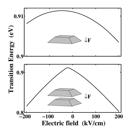
The single dot exhibits a nearly perfect quadratical dependence on the electric field which is referred to the conventional quantum confined Stark effect and has been observed in many other types of quantum structures [8, 9, 10]. The maximum transition energy occurs at kV/cm because this homogeneous InAs SAD has a positive electron-hole alignment, i.e., the hole is at the bottom of the dot for zero electric field. The stacked structure shows piecewisely quasi-linear dependence, with a turning point at a smaller negative electric field kV/cm. The lower panel of Fig. 1 shows that this discrepancy from the conventional quantum confined Stark effect occurs over the whole range of electric field, i.e., for kV/cm kV/cm. In addition, the stacked structure exhibits a Stark shift of one order of magnitude stronger than the single dot. We also notice that the maximum transition energy for both systems are roughly identical, because in the stacked structure, despite the downshift of the electron states due to tunnel coupling, the hole states are characterized by an up-shift in energy due to the strain distribution (see Fig. 2). Similar simulations have been performed for stacked structures with different sizes, different thicknesses of the coupling region, and with or without wetting layers, where the same kind of anomalous quantum confined Stark effect has been found [16].
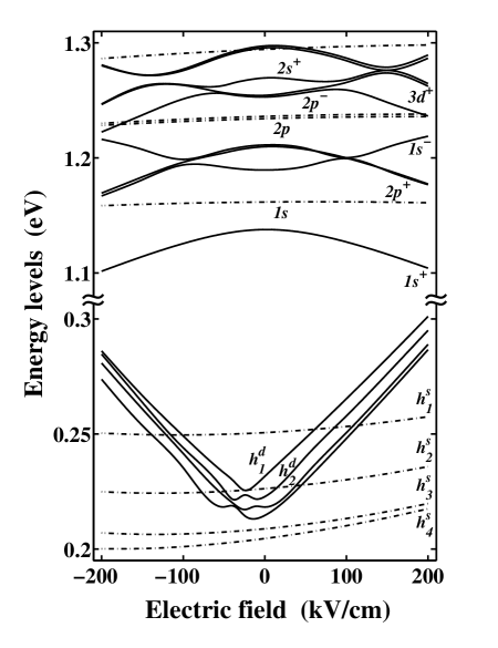
Fig. 2 shows the energy levels of the stacked structure, for both electrons and holes, as a function of electric fields. All the energies are given in reference to the top of the valence bands of GaAs. For the sake of showing the fine structure of the hole spectra near zero electric field, we use an energy scale twice as small as for electrons. For comparison, the energy levels of the single dot, are shown in dash-dotted lines. It is clearly seen that, due to the coupling between the stacked structures, the double dot system exhibits much richer structure in its energy spectrum.
In the conduction band, the energy spectrum of the single dot shows the ground 1s state, the two nearly degenerate excited 2p states, and the 3d-like state with weak sensitivity to the electric field. The coupled dot system results in bonding and antibonding states originating from these states, that in the absence of electric field, are identified as where denotes bonding (antibonding) states. Except for the ground state, all the excited states are seen to have crossings or anticrossings with other states, which reorders the states at high fields. In the valence bands of the single dot, the four hole levels (, , and ) are seen to show quadratical dependence on the electric field.
The most dramatic feature in the valence bands of the stacked structure is the quasi-linear dependence of the hole levels on the electric field for intermediate and strong field intensities, especially the ground hole state . In addition, we could not find any bonding or antibonding hole states for these structure as the ground hole state and first excited state are localized in the bottom dot and the top one, respectively. However, at small electric fields, the hole levels show small fluctuations due to mutual anticrossings. It is also noticed that the magnitude of the Stark shift for holes in the stacked structure is significantly larger than in the single dot, which is responsible for the large shift in the transition energy shown in Fig. 1.
The main reason for the hole states to behave so different in the stacked structure than in the single dot is traced in the 3D strain field distribution. Fig. 3(a) shows the profiles and the corresponding contour plots (insets) for the hydrostatic (H) and the biaxial (B) components of the strain field, which are defined as
| (3) | |||
| (4) |
Fig. 3(b) shows the diagrams of the conduction and valence band edges which are given by [17]
| (5) | |||
| (6) |
where () is the conduction (valence) band offset, () is the conduction (valence) band hydrostatic deformation potential parameter, is the valence band shear deformation potential parameter. Hence, while electrons are only sensitive to hydrostatic strain, holes are also and mostly affected by biaxial strain.
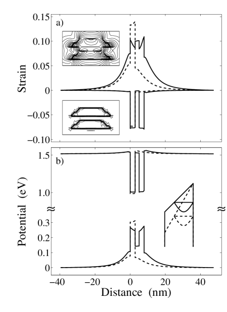
In the stacked structure, the hydrostatic negative strain field resides entirely inside the dots, and is a little stronger than in the single dot, while it almost vanishes in the coupling region (lower curve in Fig. 3a). Therefore, the coupling region is seen by electrons as a conventional tunneling barrier, which results in bonding and antibonding states as shown in Fig. 2. The biaxial positive strain field is however seen very differently in the stacked structure from that in the single dot (upper curve in Fig. 3a). First, it is smaller than in the single dot, leading to hole levels with higher energies in the stacked system (see Fig. 1). Second, unlike the hydrostatic strain, the biaxial strain retains a substantial value in the coupling region in the stacked system (top inset of Fig. 3a), which noticeably reduces the barrier height in the valence bands. Third, the biaxial strain profile in the stacked structure is inverted in the upper dot compared to the lower one although symmetric with respect to a median plane between the dots.
The most important point is that the biaxial strain defines two triangular confining potentials in each dot of the stacked structure, while in the single dot the valence band edge profile exhibits a much smoother slope (see Fig. 3b). It is seen that the strain-induced triangular potential is inverted with respect to the base in the two dots: In the bottom dot, the valence band edge is higher at the base than at the top, while it is opposite in the top dot. Therefore, the favorable combination of the lower strain-induced potential and the wider base result in a weaker hole confinement in the bottom dot than in the top dot, thereby localizing the hole ground state in the lower dot. The inset of Fig. 3(b) schematically shows the potential in the lower dot of the stacked structure together with the ground hole state at different electric fields. At zero electric field, the strain-induced built-in potential variation in the dot is meV and the ground hole state is localized approximately one fourth of the lower dot height from the bottom base.
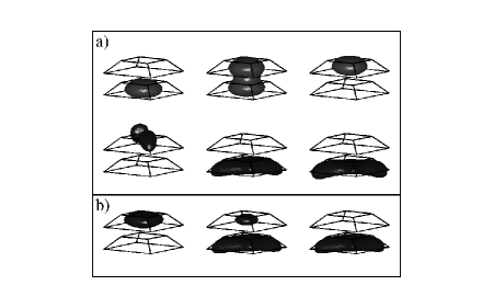
This situation is illustrated in the middle panel of Fig. 4(a) where we plot the probability density isosurfaces of ground electron and hole states at different electric fields. In contrast, it is seen that the ground electron state is the bonding state extending quasi-equally in both dots and in the coupling region. Under strong positive electric field, the ground electron state is seen in the right panel of Fig. 4(a) to become a -like state entirely localized in the upper dot. However, the ground hole state is found to behave very differently. Because the hole state is localized inside this triangular potential, as schematically shown in the inset of Fig. 3(b), its energy level changes approximately by the same amount as external variation in the dot, i.e., the potential drop arising from the external electric field [18]. For example, the variation of ground hole state energy between kV/cm and zero field is about meV, which is about the same value as the potential drop over the bottom dot caused by electric field kV/cm. Therefore it is seen in Fig. 2 that the energy of the hole state has an almost linear dependence on the electric field. This also explains the quasi-linear dependence of the ground state transition energy as shown in Fig. 1.
In Fig. 3(b), the ratio between the tunneling barrier and band offset in the valence bands is much smaller than that in the conduction bands. Consequently, it is much easier for holes to tunnel through the barrier at negative electric fields than electrons. Fig. 4(b) illustrates the transition of the ground hole state from the bottom dot to the top one occuring at a small negative electric field kV/cm. As the biaxial strain field has different distribution in the respective dots, the hole states exhibit different probability density profiles when localizing in different dots. In Fig. 2, this transition is seen as an anticrossing between the ground hole state and the first excited state, which also accounts for the anomalous quantum confined Stark effect.
Although the anomalous quantum confined Stark effect invalidates Eq. (1) over the whole range of electric field, it is possible to write two separate equations that describe the dependence of the transition energy on electric field for the stacked structure, except for the electric fields at which anticrossings occur.
| (7) | |||
| (8) |
where is a fitting parameter, is for kV/cm, and is for kV/cm.
For the right branch, nm is the built-in dipole moment of the stacked structure at zero field. From the middle panel of Fig. 4(a), the ground electron and hole states are seen to be separated by a distance larger than the coupling region ( nm), and much larger than the electron-hole separation in the single dot, which results in a dipole moment of more than one order of magnitude larger than that in the single dot. For the left branch, nm has a positive sign because of the inverted electron-hole alignment [15] in the stacked structure at negative electric fields.
The quantum confined Stark effect coefficient is defined by where () can be related to oscillator strength of optical intraband transitions in conduction (valence) bands [8, 16]. For instance, is given by
| (9) |
where is the bare electron mass, is the oscillator strength for the intraband transition from the ground state to the n-th state, with polarization along direction. has a similar expression. Single SAD structures have been shown to have very weak -polarized intraband transitions [19], therefore both and are small. In the stacked structure, the strengths of the -polarized intraband transitions in the valence bands are similar to those in the single dot. i.e., is small, which could be observed in Fig. 2 where the hole state energies show a quasi-linear dependence on the electric field. However, in the conduction bands of the stacked structure, there are several strong intraband transitions, especially the transition [19]. This results in a much larger than in single dots, and explains the magnitude of the quantum confined Stark effect coefficients in both branches () which are six times larger than in single dots, and are responsible for the ‘bowing’ of the Stark shift in Fig. 1.
In conclusion, we have shown that vertically stacked InAs/GaAs self-assembled quantum dots exhibits, in addition to a much larger Stark shift than single dots, a strong non-parabolic dependence of interband transition energy on the electric field, not been encountered in other types of quantum structures. We have demonstrated that the 3D distribution of the biaxial strain field is mainly responsible for this anomalous quantum confined Stark effect.
Acknowledgements.
This work is supported by Army Research Office, grant #DAAD 10-99-10129 and National Computational Science Alliance, grant #ECS000002N.REFERENCES
- [1]
- [2] D. Bimberg, et al., Quantum Dot Heterostructures (John Wiley & Sons, UK, 1998), see also L. Jacak, et al., Quantum Dots (Springer, Berlin, 1998).
- [3] Y. Ebiko, et al., Phys. Rev. Lett. 80, 2650 (1998).
- [4] O. Stier, et al., Phys. Rev. B 59, 5688 (1999).
- [5] I. Kegel, et al., Phys. Rev. Lett. 85, 1694 (2000)
- [6] D. L. Huffaker, et al., Appl. Phys. Lett. 73, 2564 (1998).
- [7] P. W. Fry, et al., Phys. Rev. Lett. 84, 733 (2000).
- [8] J.A. Barker, et al., Phys. Rev. B 61, 13840 (2000).
- [9] E. E. Mendez, et al., Physica B 117, 711 (1983), see also D. S. Chemla and D. A. B. Miller, Heterojuction B and Discontinuities: Physics and Device Applications (North Holland, Amsterdam, 1987).
- [10] M.-E. Pistol, et al., Phys. Rev. B 50, 11738 (1994)
- [11] H. Eisele, et al., Appl. Phys. Lett. 75, 106 (1999)
- [12] T. B. Bahder, Phys. Rev. B 41, 11992 (1990).
- [13] L. R. C. Fonseca, et al., Phys. Rev. B 58, 9955 (1998)
- [14] C. Pryor, Phys. Rev. B 57, 7190 (1998).
- [15] W. Sheng and J.-P. Leburton, Phys. Rev. B, 63, 161301R (2001).
- [16] W. Sheng and J.-P. Leburton, unpublished.
- [17] T. B. Bahder, Phys. Rev. B 45, 1629 (1990).
- [18] In a one-dimensional triangular potential created by an electric field , the ground state is an Airy function with energy . Here, we found , which is due to the 3D nature of the potential, as well as to the fact that its profile is not entirely linear.
- [19] W. Sheng and J.-P. Leburton, Appl. Phys. Lett. 78, 1258 (2001).