[
Spin-polarized transport in inhomogeneous magnetic semiconductors: theory of magnetic/nonmagnetic p-n junctions
Abstract
A theory of spin-polarized transport in inhomogeneous magnetic semiconductors is developed and applied to magnetic/nonmagnetic p-n junctions. Several phenomena with possible spintronic applications are predicted, including spinvoltaic effect, spin valve effect, and giant magnetoresistance. It is demonstrated that only nonequilibrium spin can be injected across the space-charge region of a p-n junction, so that there is no spin injection (or extraction) at low bias.
pacs:
72.25.Dc,72.25.Mk] Semiconductor spintronics is a developing field where active control of spin dynamics is projected to lead to device applications with more functionality and better integrability with traditional semiconductor technology than metal-based spintronics [3]. Spin injection into a semiconductor has been demonstrated [4, 5], but an important question, what this injected spin is useful for, remains largely unanswered (though some semiconductor spintronic device schemes have been proposed [6, 7]). This Letter addresses the problem of spin and charge bipolar (electron and hole) transport in inhomogeneously doped magnetic semiconductors (such as BeMnZnSe, CdMnSe, or GaMnAs, whose carrier -factors are large due to magnetic doping). We show, as an important consequence of our theory, that a magnetic/nonmagnetic p-n junction has significant potential for device applications, and predict large magnetoresistance for such a junction. We also show that the magnetic junctions display spinvoltaic and spin valve effects: a current, whose direction changes with the direction of applied magnetic field or injected spin polarization, can flow without any applied bias. These effects should be useful for sensing magnetic fields, and for probing spin polarization and spin relaxation.
To introduce the equations for spin and charge bipolar transport in inhomogeneously doped magnetic semiconductors, consider a semiconductor doped with acceptors and donors, and with magnetic impurities, whose density varies in space and whose presence leads to large -factors for electrons and holes, and . In a homogeneous magnetic field the carrier energies are Zeeman-split: spin up ( or ) and spin down ( or ) electrons have their energy shifted by , where is Bohr magneton and is the proton charge; the energy of holes changes by . Carrier charge current densities, resulting from the electric field , nonuniform magnetic “potentials” , electron (hole) densities (), are
| (1) | |||||
| (2) |
where and stand for mobility and diffusivity, and the “magnetic” drift forces carriers with opposite spins to go in opposite directions. The above equations follow from the requirement that carrier densities in an inhomogeneous environment have the quasiequilibrium form, for example, , where is the number of electrons per spin at (nonequilibrium) chemical potential , and the expression for the current [8]. From Eqs. 1 and 2, the carrier charge and spin current densities and are:
| (3) | |||||
| (4) |
and
| (5) | |||||
| (6) |
Here and , and we introduced electron charge and spin conductivities and , where and , and similarly for diffusivities. Analogous notation is used for holes. Equations 3-6, which are a generalization of the Johnson-Silsbee magnetotransport equations [9], reflect the spin-charge coupling in bipolar transport in inhomogeneous magnetic semiconductors: a spatial variation in spin density, as well as in , can cause charge currents, and spin currents can flow as a result of a spatial variation of carrier densities and .

Generation and recombination of electrons and holes are assumed to be mostly due to band-to-band processes. Furthermore, electrons (holes) with a given spin are assumed to recombine with holes (electrons) of either spin. The stationary continuity equations for electrons and holes read
| (7) | |||||
| (8) |
Here and are the equilibrium carrier densities, is the (generally spin dependent) band-to-band recombination rate, and is the spin relaxation time. Spin relaxation equilibrates electron spins while preserving nonequilibrium electron density, so, for a nondegenerate semiconductor, , where is the equilibrium electron spin polarization (, with being the Boltzmann constant and temperature). In general, , where is obtained from the known nonequilibrium electron density ; similarly for holes. To include transient effects, terms and need to be added to the left sides of Eqs. 7 and 8.

Equations 1 and 2 (or, 3-6), 7 and 8, and Poisson’s equation , where and is the dielectric constant of the semiconductor, determine the distributions of charge and spin in a magnetic semiconductor under applied bias V. For ferromagnetic semiconductors needs to be evaluated self-consistently (similarly to ). Indeed, the magnetization depends on the carrier density (as the mobile carriers mediate the magnetic interactions), and the carrier density depends on magnetization, as magnetization determines .
We have made a number of simplifying assumptions in our theory which are not strictly valid in real magnetic semiconductors such as GaMnAs. For example, electron and hole band states are treated as simple spin doublets, although the band structure is usually more complicated in the presence of spin-orbit coupling. We also do not take into account the fact that magnetic impurities change the gap and can offset the bands, even at B=0. Finally, in some magnetic semiconductors (even nonferromagnetic) carrier densities may strongly affect the response of the magnetic ions to magnetic field, in which case a selfconsistent calculation is needed. In principle, our formalism can be tailored to include these more complicated effects, but this can only be done on a case-by-case basis (if the effects are well understood, which is currently not the case). Our approach here is to consider a simple but reasonable model to illustrate new phenomena that can occur in inhomogeneous magnetic semiconductors.
We now apply the above theory to the problem of a magnetic/nonmagnetic p-n junction, with only electrons being magnetically active () [10]. Two cases are considered (Fig. 1): (i) the magnetic -side to study spin injection, and (ii) the magnetic -side, to study spin extraction and magnetoresistance phenomena. We assume perfect ohmic contacts (both carriers and spins at equilibrium) as boundary conditions, except when we study the dependence of the current on nonequilibrium spin (in which case we keep the ohmic contacts for carrier densities only, not for the spin). We only deal with nondegenerate semiconductors, as these are analytically tractable, and yield the largest magnetoresistance.

To be specific, we consider a m long GaAs p-n junction at room temperature, doped with cm-3 acceptors to the left, cm-3 donors to the right [7], and with magnetic impurities inducing electronic -factor which follows the shape of () for the magnetic () region. Holes are unpolarized, so we omit the label when dealing with spin-related quantities, and reserve that symbol for the -region-related variables. Figure 1 depicts our geometry and the distribution of electrons and holes for various cases considered below. The materials parameters [11] are the electron and hole diffusivities, cm2s-1, and mobilities cmVs-1. The intrinsic (nonmagnetic) carrier density is cm-3, the dielectric constant of the vacuum permittivity; the calculated built-in-voltage is V at . Recombination rate cms-1, and the spin relaxation time ns. The minority [12] diffusion lengths are [7] m, m, and the electron spin diffusion length in the () region is m (=0.8 m). Figure 2 illustrates the doping profile and a typical profile of carrier and spin densities.
We first ask the important question whether spin can be injected and extracted into/from the nonmagnetic region. Figure 3 shows the results of our numerical calculations, where we plot spin polarization (note that we are interested here in spin polarization of density, not current [7]). At small bias (below the built-in-value), which is also the small injection limit, there is no significant spin injection or extraction. As the bias increases, the injection and extraction become large and intensify with increasing . The reason why there is no spin injection (and, similarly, extraction) at small bias is that although there are exponentially more, say, spin up than spin down electrons in the magnetic side, the barrier for crossing the space-charge region is exponentially larger for spin up than for spin down electrons (see Fig. 1). Those two exponential effects cancel each other, so there is no net spin current flowing through the space-charge region. The numerical aproach is indispensible for obtaining the high-injection results, where we observe a large nonequilibrium spin polarization around the space-charge region, resulting in spin injection and extraction.
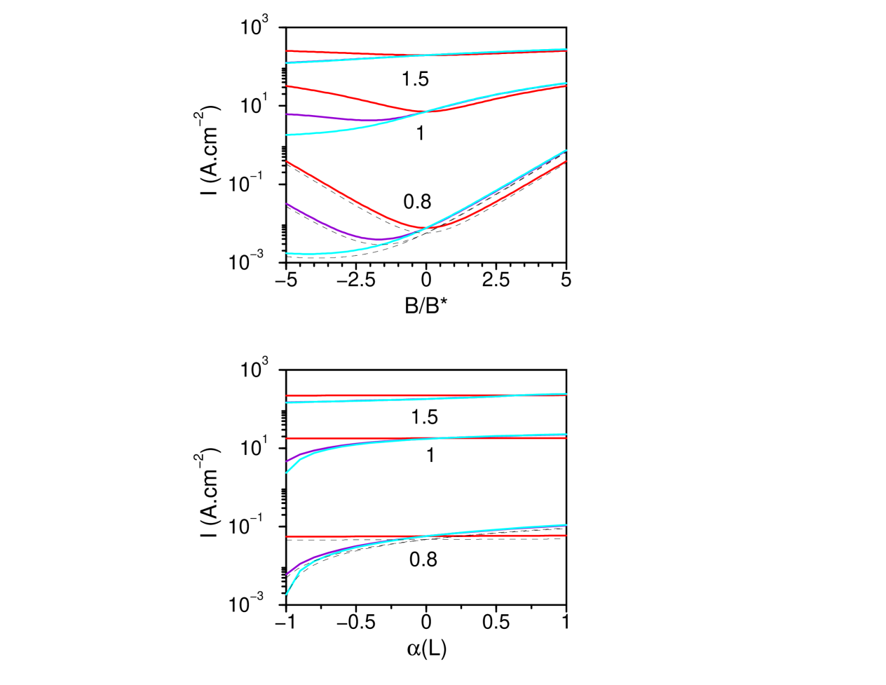
The current through a magnetic/nonmagnetic p-n junction depends on magnetic field. This dependence has two sources. First, a magnetic field makes the band gap spin dependent, leading to the increased density of the minority carriers. For example, the equilibrium density of electrons in a magnetic -region (Fig. 1C) is (in equilibrium, from Boltzmann statistics). The current through a p-n junction is proportional to the density of the minority (not majority) carriers, and so it will grow exponentially with for . This does not happen for unipolar transport (a homeogenous sample), where the current depends on the density of the majority carriers, which is independent of , as it is fixed by the number of ionized impurities. The exponential magnetoresistance for the system in Fig. 1B is shown in Fig. 4. The effect diminishes with increasing bias. The second way a current can depend on is if a nonequilibrium spin with polarization is introduced (optically or by spin injection) into the sample (Fig. 1C and D). The exponential magnetoresistance becomes giant (meaning, the resistance changes when the orientation of the magnetic moment in the magnetic region with respect to the orientation of the injected spin in the nonmagnetic region, changes) as seen in Fig. 4. The current is exponentially sensitive to both and , being large (small) if they are of the same (opposite) sign.
To explain analytically our numerical results, we generalize the well-known Shockley approximation [8] for the p-n junction to include nonequilibrium spin, which is given, in the quasi-neutral regions, by the spin-diffusion equation
| (9) |
where , of which is the solution of the corresponding carrier diffusion equation. We consider the magnetic -region, and impose a nonequilibrium spin polarization at the right boundary (see Fig. 1C, where also the boundary points used below are indicated). We postulate as the second boundary condition for spin, in the spirit of the quasiequilibrium approximation [8], that spin current vanishes at , the -side boundary of the space-charge region. The spin polarization in the -region is
| (10) |
where and . At , ; it vanishes if , in line with our result of no spin extraction at low bias. In the -region (ohmic boundary condition for spin) and the second boundary condition, that at , the -side boundary of the space-charge region, which can be obtained from the usual quasiequilibrium condition of constant chemical potentials (applied to nondegenerate statistics) from to , is . The nonequilibrium minority carrier density at is . With these boundary conditions the carrier and spin profiles in the magnetic -region are
| (11) | |||||
| (12) |
Having the profiles, we calculate the current in the magnetic p-n junction. We distinguish equilibrium-spin electron and hole currents, and nonequilibrium-spin-induced current , so that the total charge current is . The individual contributions are
| (13) | |||||
| (14) | |||||
| (15) |
Figure 4 shows how well this analytical model compares with our numerical calculation. The small discrepancy is caused by the neglect of the recombination processes inside the space-charge region; the model breaks down at large bias, where the Shockley approximation becomes invalid [8]. We note that if the spin is injected by the bias contact at , one needs to consider a model in which depends on (since it then obviously vanishes at ), and solve Eqs. 13-15 for . Otherwise the above equations describe either the case of an independent spin injection, or the region of where is independent of .
The large exponential magnetoresistance effect, at large (or ), comes from the increase of the minority electron population with . However, once a nonequilibrium spin population (finite ) is maintained with its sign fixed in the space-charge region, a giant magnetoresistance (GMR) should be observed, at large and . The GMR coefficient is then . In addition to sensing , these effects can be used for an all-electrical probing of the injected spin polarization and spin diffusion length , as they both determine (a similar device scheme is proposed in Fig. 1 D). The key to employing the large magnetoresistance effects in spintronics is the development of materials with large -factors. Even for , the GMR coefficient at K and T is about , which is close to 200%. A magnetic impurity that would give would yield 2,500 %, (300% at room temperature). The device potential of magnetic p-n junctions is enormous, but to take full advantage we need materials with large -factors at room temperature [13].
Equations 13-15 reveal another interesting phenomenon, a spinvoltaic effect. While both and vanish for , stays finite, if . A current flows at zero bias! This is an analogue of the photovoltaic effect, where a reverse current can flow by introducing photogenerated carriers into the space charge region. In the spinvoltaic effect both reverse and forward currents can flow, depending on the relative orientation of and , so a magnetic p-n junction can act as a spin valve. The physics of the spinvoltaic effect is that nonequilibrium spin in the space-charge region disturbs the balance between the generation and recombination currents (Fig. 1C). If , and more spin up electrons are present at (), the barrier for them to cross the region is smaller than the barrier for the spin down electrons, so more electrons flow from to than from to , and positive charge current results. If there are more spin down electrons at (), the current is reversed. We note that, as at no spin can be injected by the ohmic contact into the region, the nonequilibrium spin population has to be injected either optically (at a distance larger than but smaller than from the space-charge region), or electronically transverse to the flow of (and also within of the space-charge region).
In summary, we have explored bipolar magnetotransport in magnetic/nonmagnetic p-n junctions, which are of great potential for emerging semiconductor spintronics. We have used a simple model to describe the new physics that results when the magnetotransport is dominated by minority, rather than majority charge carriers. In particular, we find that spin injection is suppressed at low biases, because the spin-dependent barrier to transport in the depletion layer negates the effect of spin polarization of the carriers. Furthermore, we predict exponential magnetoresistance resulting from the magnetic field dependence of the population of the minority carriers, and giant magnetoresistance, appearing if the polarization of the majority carriers is disturbed externally (by a third-terminal spin injection, for example). We also find that a nonequilibrium spin-polarized population can lead to a charge current–a spinvoltaic effect. Finally, we have shown that at small biases the effects of interest can be described by a modified Shockley model.
This work was supported by DARPA and the US ONR.
REFERENCES
- [1]
- [2] Current address: Institute for Theoretical Physics, Karl-Franzens University, Universitatsplatz 5, 8010 Graz, Austria.
- [3] S. Das Sarma, J. Fabian, X. Hu, and I. Žutić, IEEE Transaction on Magnetics 36, 2821 (2000); Superlattice Microst. 27, 289 (2000); Solid State Commun. 119, 207 (2001).
- [4] R. Fiederling, M. Kleim, G. Reuscher, W. Ossau, G. Schmidt, A. Waag, and L. W. Molenkamp, Nature 402, 787 (1999); Y. Ohno, D. K. Young, B. Beschoten, F. Matsukura, H. Ohno, and D. D. Awschalom, Nature 402, 790 (1999); B. T. Jonker, Y. D. Park, B. R. Bennett, H. D. Cheong, G. Kioseoglou, and A. Petrou, Phys. Rev. B 62, 8180 (2000).
- [5] P. R. Hammar, B. R. Bennett, M. J. Yang, M. Johnson, Phys. Rev. Lett. 83, 203 (1999); V. P. LaBella, D. W. Bullock, Z. Ding, C. Emery, A. Venkatesan, W. F. Oliver, G. J. Salamo, P. M. Thibado, and M. Mortazavi, Science 292, 1518 (2001).
- [6] S. Datta and B. Das, Appl. Phys. Lett. 56, 665 (1990); M. E. Flatte and G. Vignale, Appl. Phys. Lett. 78, 1273 (2001).
- [7] I. Žutić, J. Fabian, and S. Das Sarma, Phys. Rev. B 64, 121201 (2001); Appl. Phys. Lett. 79, 1558 (2001).
- [8] S. Tiwari, Compound Semiconductor Device Physics (Academic Press, San Diego, 1992).
- [9] M. Johnson and R. H. Silsbee, Phys. Rev. B 35, 4959 (1987); J.-E. Wegrove, Phys. Rev. B 62, 1067 (2000).
- [10] We neglect hole spins in our model for the sake of clarity so that we illustrate the results on one carrier type. It is straightforward to include hole spin transport (especially in our analytical formulas).
- [11] Chosen to have typical values for GaAs with no special significance about the numbers we use.
- [12] Term minority (majority) referes to the relative population of electrons and holes.
- [13] At low temperature, this is already acheived, g500 in (Cd0.95Mn0.05Se):In. T. Dietl, in Handbook of Semiconductors Vol. 3, edited by T. S. Moss and S. Mahajan, p. 1279 (Noth-Holland, New York, 1994).