Nature 410, 444 (March 22, 2001).
Stable ultrahigh-density magneto-optical recordings using introduced linear defects
The stability of data bits in magnetic recording media [1, 2] at ultrahigh densities is compromised by thermal ‘flips’ – magnetic spin reversals – of nano-sized spin domains [3], which erase the stored information. Media that are magnetized perpendicular to the plane of the film, such as ultrathin cobalt films or multilayered structures [4, 5], are more stable against thermal self-erasure [2, 6] than conventional memory devices. In this context, magneto-optical memories seem particularly promising for ultrahigh-density recording on portable disks, and bit densities of 100 Gbit inch-2 (ref. [7]) have been demonstrated using recent advances in the bit writing and reading techniques [7, 8, 9, 10, 11]. But the roughness and mobility of the magnetic domain walls [12, 13] prevents closer packing of the magnetic bits, and therefore presents a challenge to reaching even higher bit densities. Here we report that the strain imposed by a linear defect in a magnetic thin film can smooth rough domain walls over regions hundreds of micrometers in size, and halt their motion. A scaling analysis of this process, based on the generic physics of disorder-controlled elastic lines [14, 15, 16, 17], points to a simple way by which magnetic media might be prepared that can store data at densities in excess of 1 Tbit inch-2.
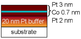
Increasing information storage to densities past 100 Gbit inch-2 may evolve through extensions of current magnetic recording technologies (to patterned media [6], for example). But such increases in storage density might be achieved by using other techniques such as holography (via interference patterns produced by two intersecting laser beams) [18], or micromachined nano-cantilever arrays [19], or – to satisfy a relentless demand for portability – using scanning localized subwavelength () (near-field) optical probes [9] that can imprint and resolve images in magneto-optic media [8] of the order of the probe size. The bit-writing with local probes may be thermally assisted by a current [20] or a laser beam that raises local temperature to the vicinity of the Curie temperature , resulting in the formation of a reversed domain with a rough wall. To realize smooth and (for precise positioning) stable (‘noiseless’) domain walls that can be implemented without, for example, nanoscale patterning, we suggest a conceptual identification of walls with elastic lines [16] and seek to utilize linear defects inducing a directional long-range strain field in ultrathin Pt/Co/Pt structures – long considered excellent candidates for high-density recording at blue-range wavelengths [11]. In such trilayers (Fig. 1), large uniaxial perpendicular anisotropy is sustained by the interface contribution up to Co thickness 1.5 nm; beyond this thickness the magnetizaton switches from out-of-plane to in-plane [5].
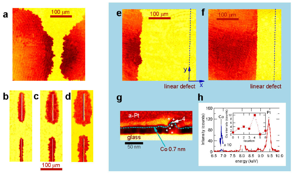
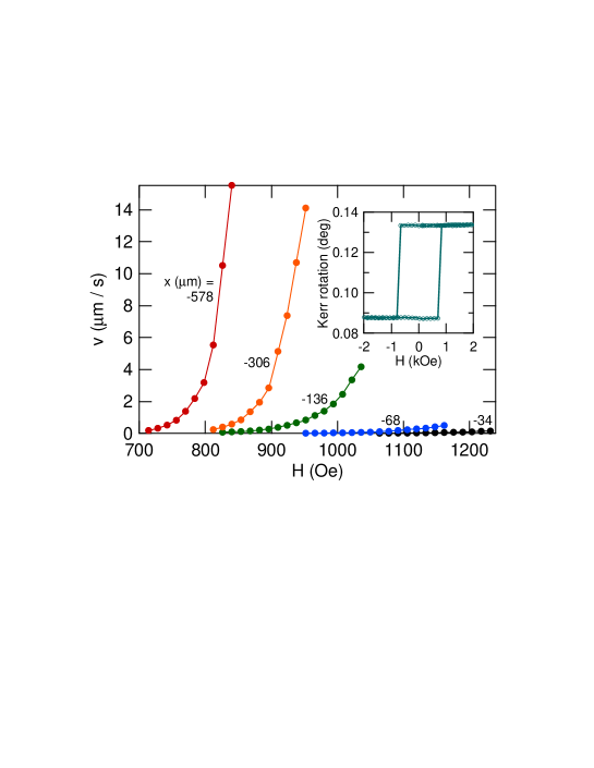
Figure 2a shows two typical up-domains (see legend for imaging details [21]), nucleated owing to a locally suppressed coercive field [3] in a 0.7 nm Co film sandwiched between 3 nm (top) and 2 nm (bottom) Pt layers, prepared using standard deposition parameters [22] and without linear defects. The domains are round with (undirected) domain walls (DWs) that are as rugged as expected [12]. We note that patterned nucleation sites, as in Fig. 2b-d, do not reduce either DW roughness or velocity. As magnetic field is increased beyond Oe (inset in Fig. 3), the outward motion of DWs becomes increasingly swift (estimated from displacement of a small segment of the wall during 500-ms field pulses, the wall velocity is more than m s-1 at Oe).
To control the rugged DW structure we will use a recently found connection between the DW behavior in thin films [13] and that of elastic lines [14, 15, 16]. One prominent example of directed elastic lines are wandering vortex lines (quantized magnetic flux lines maintained by a swirling tube of current) in high temperature superconductors [16] that can be strongly localized by interaction with columnar (linear) defects [17]. A powerful arsenal of ideas can now be engaged to understand how a linear defect potential may localize and reduce the roughness of DWs, and force them to accommodate to the defect shape. We introduce a line defect that delivers a three-punch action. Through magneto-elastic coupling, (i) it gives the wall a preferred direction [14] (along the defect), (ii) it increases its elasticity, reducing the DW roughness as it negotiates the random landscape, and (iii) it acts to reduce wall velocity to a nearly full stop in fields greater than the coercive field of unmodified film. The defect is installed during the Co deposition by imposing an anisotropic tension (clamping) on the substrate and its subsequent release [23]. The resulting Co ‘fold’ (Fig. 2g,h) introduces a -axis invariant long-range strain field .
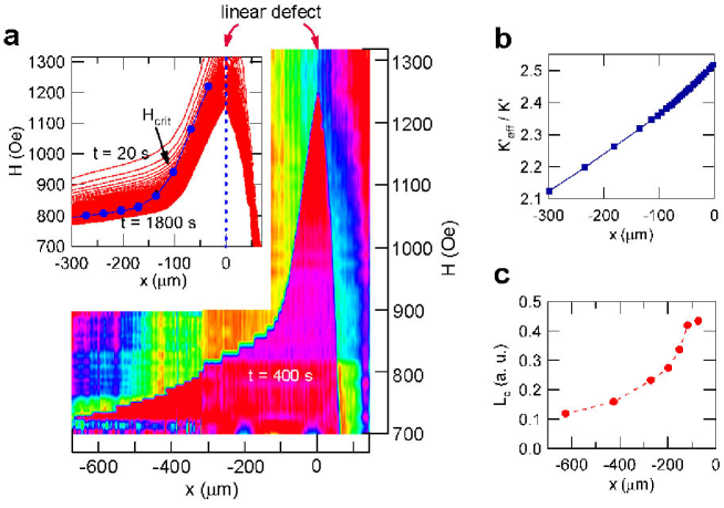
A DW driven by the magnetic field toward such linear defect (Fig. 2e,f) presents a structural contrast with the DWs in the unmodified film in Fig. 2a. Even at large distances (m) away from the defect, the DW conforms on the average to the defect line along . It becomes progressively smoother (and straighter) as it approaches the defect. It also rapidly decelerates. The deceleration and near-standstill of the wall depends on the proximity to the defect, as represented by the spatial progression of the velocity-versus-field (force) response in Fig. 3. The - curves are highly nonlinear, as has been reported recently in Co films [13] where the disorder landscape is formed, for example, by atomic scale imperfections at the film–substrate interface. Such nonlinear response in the limit of vanishing driving force is a signature of glassy (creep) dynamics [24], well established for the elastic vortex lines in a superconductor through measurements of the voltage-versus-current (-) characteristics [16]. Above (obtained from the - curves by the usual velocity cut-off criterion, here chosen at m s-1) the driving field exceeds the ‘pinning’ force [16] and the DW response becomes linear and faster. We note that DW velocity, even far away from a line defect, is orders of magnitude lower than in unmodified films. Figure 3 shows a field-forward advance of - curves to higher fields, and an enhanced (often referred to as a ‘propagation field’ [3]) on the approach to the line defect. An effective potential well that localizes the wall is formed by the driving field pushing the wall and the line-defect that acts against this push. It resembles columnar defects in a superconductor, where the critical current is enhanced [17]. correlates with the long-range repelling force field exerted on the DWs by the line-defect, whose spatial extent is mapped in Fig. 4a. The shape of – a ridge along – is either extracted directly from Kerr images taken with increasing after a fixed propagation time (main panel), or more quantitatively from the averaged DW positions versus time at all fields. As illustrated in the inset, it takes a higher field to get closer to the line-defect; but at any , after s, two DWs – one approaching the ridge from the left and another from the right – become effectively stationary.
Within the elastic description of a DW, the relevant scale is a collective pinning [24] length , where and are characteristic size and strength of underlying random disorder, and is the wall energy. At lengths , the wall will elastically adjust to the random landscape to nestle in a local minimum energy configuration. The DW energy density (in addition to a uniform field term and ignoring a weak dipolar term) can be written as a sum of three: the exchange energy , the anisotopy energy , and the magneto-elastic energy [25] coupling to the strain generated by the line-defect,
| (1) |
Here is the exchange stiffness [3], ( is the anisotropy constant and is Pt-polarization-enhanced saturation magnetization of Co), and is related to Young’s modulus of the film. Magnetization rotates from ‘up’ to ‘down’ within the wall thickness (we estimate at 3 nm) and the wall (in the simplest form) is of Bloch type [13], where the azimuthal angle and the rotation is parameterized by an angle between the -axis and ( is the direction cosine along ). Minimizing leads to DW energy [3] , where . The total wall energy (per unit area) in a magnetic field is . From the stability condition we obtain a nonlinear differential equation for : , which we solve numerically using the stationary mapped in Fig. 4a. The result is a factor of enhanced effective anisotropy (Fig. 4b) and, consequently, an enhanced DW elastic energy (per unit length) [13] . Thus, the enhanced elasticity of DW is in part responsible for the longer . The longer is a key to the reduced DW roughness. This can be seen from the analysis of transverse displacements of the domain wall segments by computing from the DW images a (line shape) correlator [14] , predicted for to scale as [16] . We find that the characteristic length is enhanced in the vicinity of the line-defect by a factor of (Fig. 4c). This implies a reduction of roughness, as measured by , by a factor of on the shortest length scales and hence a potential increase in the areal density by nearly two orders of magnitude. In its proximity, the line defect wins over randomness so that on sufficiently long distances along its length DWs become essentially ‘flat’ (that is, finite for ) [14] in fields up to . The wall-smoothing at higher fields and at speeds of current recording technology (Gbit s-1) deserves further study for practical implementations of this effect. The long-range strain associated with a line defect presents an efficient, and relatively simple and cost-effective control of domain walls, with only a few such defects needed to stabilize large areas of ultrathin films.
REFERENCES
- [1] Magnetic Recording: The First Hundred Years. Eds. Daniel, E.D., Mee, C.D. & Clark, M.H. (IEEE Press, New York, 1998).
- [2] Thompson, D.A. & Best, J.S. The future of magnetic data storage technology. IBM J. Res. Develop. 44, 311-322 (2000).
- [3] Hubert, A. & Schäfer, R. Magnetic domains (Springer, New York, 1998).
- [4] Kirby, R.D., Shen, J.X., Hardy, R.J. & Sellmyer, D.J. Magnetization reversal in nanoscale films with perpendicular anisotropy. Phys. Rev. B 65, R10810-13 (1994).
- [5] Allenspach, R., Stampanoni, M. & Bischof, A. Magnetic domains in thin epitaxial Co/Au(111) films. Phys. Rev. Lett. 65, 3344-47 (1990).
- [6] Weller, D. & Moser, A. Thermal effect limits in ultrahigh density magnetic recording. IEEE Trans. Magn. 35, 4423-39 (1999).
- [7] Partovi, A. Optical near-field aperture storage technique for high density, high performance data storage applications. SPIE 3864, 352-354 (1999).
- [8] Awano, H. & Ohta, N. Magnetooptical recording technology toward 100 Gb/in2. IEEE J. Selected Topics in Quantum Electronics 4, 815-820 (1998).
- [9] Betzig, E., Trautman, Harris, T.D., Weiner, J.S. & Kostelak, R.L. Breaking the diffraction barrier: optical microscopy on a nanometer scale. Science 251, 1468-1470 (1991).
- [10] Partovi, A. et al. High-power laser light source for near-field optics and its application to high-density optical data storage. Appl. Phys. Lett. 75, 1515-17 (1999).
- [11] Kaneko, M. Magnetic multilayer films for high density magneto-optical recording. J. Magn. Magn. Mater. 148, 351-356 (1995).
- [12] Han, S.K, Yu, S.-C. & Rao, K.V. Domain wall jaggedness induced by the random anisotropy orientation in magneto-optic materials: A computer simulation study. J. Appl. Phys. 79, 4260-64 (1996).
- [13] Lemerle, S. et al. Domain wall creep in an Ising ultrathin magnetic film. Phys. Rev. Lett. 80, 849 (1998).
- [14] Halpin-Healy, T. & Zhang, Y.-C. Kinetic roughening phenomena, stochastic growth, directed polymers and all that. Phys. Rep. 254, 215-414 (1995).
- [15] Hwa, T. From vortices to genomics. Nature 399, 17-18 (1999).
- [16] Blatter, G., Feigel’man, M. V., Geshkenbein, V. B., Larkin, A. I. & Vinokur, V. M. Vortices in high-temperature superconductors. Rev. Mod. Phys. 66, 1125 (1994).
- [17] Krusin-Elbaum, L. et al. Superconductivity enhanced by Hg fission. Nature 389, 243-244 (1997).
- [18] Heanue, J.F., Bashaw, M.C. & Hasselink, L. Volume holographic storage and retrieval of digital data. Science 265, 749-752 (1994).
- [19] Binnig, G.K., Rohrer, H. & Vettiger, P. Mass-storage applications of local probe arrays. U.S. Patent 5,835,477, November 10, 1998.
- [20] Nakamura, J., Miyamoto, M., Hosaka, S. & Koyanagi, H. High-density thermomagnetic recording method using a scanning tunneling microscope. J. Appl. Phys. 77, 779-81 (1995).
- [21] Argyle, B.E. & McCord, J.G. New laser illumination method for Kerr microscopy. J. Appl. Phys. 87, 6487- 6489 (2000).
- [22] Weller, D. et al. Ion induced magnetization reorientation in Co/Pt multilayers for patterned media. J. Appl. Phys. 87, 5768-70 (2000).
- [23] Deng, H., Jarratt, J.D., Minor, M.K. & Barnard, J.A. Artificially controlled stress anisotropy and magnetic properties of FeTaN thin films. J. Appl. Phys. 81, 4510-12 (1997).
- [24] Feigel’man, M. V., Geshkenbein, V. B., Larkin, A. I. & Vinokur, V. M. Theory of collective flux creep. Phys. Rev. Lett. 63, 2303-2306 (1989).
- [25] Chuang, D.S., Ballentine, C.A. & O’Handley, R.C. Surface and step magnetic anisotropy. Phys. Rev. B 49, 15084-15095 (1994).
Acknowledgements
We thank J. Slonczewski, V. Vinokur, G. Blatter, and G. Zimanyi for useful discussions. Correspondence and requests for materials should be addressed to L. Krusin-Elbaum, fax: +1-914-945-2141; e-mail: krusin@us.ibm.com.
∥ present address: Seagate Technology, Pittsburgh, PA 15203, USA.