Microstructure of the highly dense MgB2 superconductor by transmission electron microscope
Abstract
The microstructure of the MgB2 superconductor sintered at high temperature under a high pressure of 3 GPa was investigated by using a high-resolution transmission electron microscope (HRTEM). The TEM images did not show any pores in the specimen. All grains were compactly connected, and no discernable empty spaces or impurities at the boundaries existed over the regions investigated. The HRTEM image showed clearly each constituent atom that formed the basal hexagonal plane, without any defect in a single grain. The a-axis lattice parameter, 0.307 nm, from this direct measurement was shorter than the value, 0.314 nm obtained from samples prepared using diffusion techniques. A minor impurity phase, which was most probably MgB4 and did not form interfacial layers was also observed, but was well isolated from the main MgB2 phase. Our results verify that the MgB2 powder was sintered under high temperature and high pressure into its theoretical density without any porosity or grain growth.
pacs:
PACS number: 74.60.-w, 74.62.Bf, 61.14.Lj, 61.16.BgSuperconductivity at about 40 K in MgB2 was announced quite recently.[1] The of this binary intermetallic superconductor is the highest among the non-oxide and non-C60-based compounds and is near the upper limit suggested by the conventional BCS theory.[2] A phonon- mediated paring mechanism has been proposed to explain the superconductivity and is supported by the observation of a boron isotope effect with an isotope exponent .[3, 4] The carrier type was predicted to be positive,[5] which was confirmed by Hall measurements.[6]
Typically, MgB2 powders have been synthesized by sintering mixtures of Mg and B powders in an inert atmosphere.[3, 7, 8] Some have reported the synthesis of high-density pellets sintered under high pressures of several GPa; this high density makes it easier to study the transport properties.[6, 9, 10] A strong connection between the grains, which increases with increasing sintering temperature under high pressure, has been suggested to explain the concurrent changes in the resistivity and the low-field magnetization.[11] The microstructure of high-density MgB2 has been observed by using a scanning electron microscope (SEM)[10, 11] or an optical microscope.[7] However, the high-resolution transmission electron microscope (HRTEM) images of MgB2 showing the detailed structure of a single grain and the grain boundary have not yet been reported.
In this paper, we report HRTEM observations of the microstructure of the high-density MgB2 superconductor. The TEM images showed that no pores existed in the specimen. All grains were well connected without any impurities at the grain boundaries, much like at the twin boundary of YBa2Cu3Oy. The HRTEM image showed each constituent atom clearly, and not a single MgB2 grain containing any impurities. An a-axis lattice parameter of 0.307 nm was obtained from this direct measurement and is shorter than the value of a = 0.314 nm obtained from samples prepared using a diffusion techniques. The minor impurity phases were well isolated from the main MgB2 phase. Our results suggest that the MgB2 powder was sintered into its theoretical density without any impurities at the grain boundaries. These properties can make the transport measurements very reliable.
A 12-mm cubic multi-anvil-type press was used for the high-pressure sintering.[9] The starting material was a commercially available powder of MgB2. The pressed pellet was placed in a Au capsule in a high-pressure cell and pressurized up to 3 GPa. While the pressure was maintained, the heating temperature was increased linearly; then, it was kept at 900∘C for 1 hour. The samples were then quenched to room temperature. The pellets, weighing about 130 mg, were about 4.5 mm in diameter and 3.3 mm in height. A TEM specimen was prepared by mechanical polishing with a Tripod polisher for precise thickness control. A specimen was polished on diamond abrasive films down to about a 10 m thickness and then ion-milled with Ar ions for 20 hours. This was done using a Gatan dual ion miller at 5 kV and 0.6 mA. A high-resolution image, a bright field image, and a selected area electron diffraction (SAED) pattern were obtained with a transmission electron microscope (JEOL JEM-2000EX) operating at 200 kV.
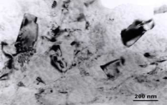
Figure 1 shows the microstructure observed using the TEM at low magnification. Surprisingly, the microstructure showed that the sample was pore-free and was almost 100% densified. The grain sizes were in the range of 300 nm to 800 nm. All grains were well connected without any impurities at the grain boundaries. Only the crystal orientation was different from grain to grain at the boundary, much like the case of the twin boundary of YBa2Cu3Oy. The dark and the light regions in Fig. 1 are from grains with different crystallographic orientations. Some elongated grains with aspect ratios of 4 to 6 were also observed.
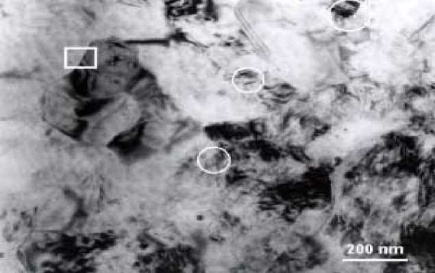
Figure 2 shows a bright-field image, mostly consisting of MgB2. Over small areas with sizes less than 100 nm, lattice fringes with an interplanar spacing larger than that of MgB2 were observed in the regions denoted by circles. Previously, two kinds of impurities, cubic MgO and orthorhombic MgB4, had been reported by Takano et al. for MgB2, sintered at high pressure.[10] In that case, a trace of MgO was present in the starting MgB2 powder, and the small amount of MgB4 originated from the partial decomposition of MgB2 to MgB4 at 1000 C under a pressure of 3.5 GPa.[10] Since the c-axis lattice constants of MgO and MgB4 are 0.4213 nm (JCPDS 04-0829) and 0.7472 nm (JCPDS 15-0299), respectively, the observed impurities seemed to be mostly MgB4 because of the large c-axis constant.
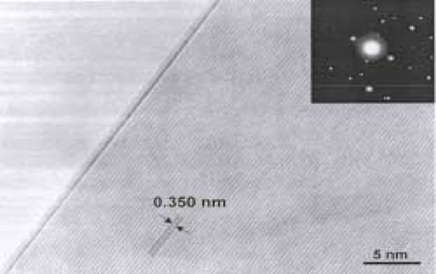
Figure 3 shows the HRTEM image of the grain boundary marked by the white square in Fig. 2. There is no visible intergranular phase at this grain boundary. The beam direction of the SAED pattern in the inset of Fig. 3 was [010], and the defect-free lattice fringe, which is due to the (001) basal hexagonal plane of MgB2. And its interplanar spacing, equivalent to the c-axis lattice parameter, was estimated to be 0.350 nm, which is same as the reported value.[3]
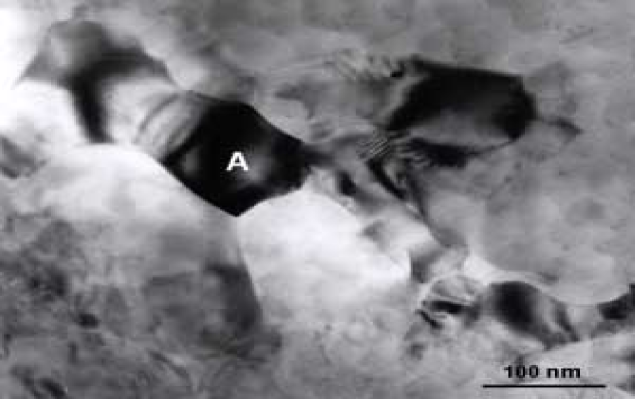
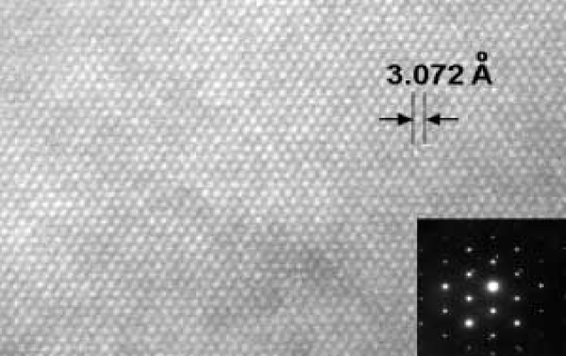
Figure 4 shows a bright-field image at high magnification. Neighter porosity Nor intergranular phase, were observed at the grain boundaries, as in Fig. 1. The MgB2 grain marked A was selected for HRTEM imaging, and that image is shown in Fig. 5. The beam direction of the SAED pattern from the grain, shown in the inset of Fig. 5, was [001], and the HRTEM image of the grain shows a very clean basal plane consisting of an Mg atomic array. The in-plane a-axis lattice parameter was estimated to be 0.307 nm, which is shorter than the value of a = 0.314 nm for samples prepared using a diffusion techniques.
In summary, we used a HRTEM to obtain the microstructure of the high-density MgB2 superconductor. No porosity and no intergranular phases were observed on the TEM images of the polycrystalline MgB2. The observed minor impurity phases, which seemed to be MgB4, were well separated from the main MgB2 phase. The lattice fringe image from the HRTEM image shows well-aligned atomic array, without any defects in a single grain, and proves that this sample is very clean. Thus, the measurements of the transport properties for our MgB2 sintered under high pressure should not be affected by impurities or defect scattering.[12]
This work was supported by the Korea Research Council for Industrial Science & Technology and the Ministry of Science and Technology through the Creative Research Initiative Program and the National Research Laboratory Program.
REFERENCES
- [1] J. Nagamatsu, N. Nakagawa, T. Muranaka, Y. Zenitani, and J. Akimitsu, presented at the Symposium on Transition Metal Oxides, Sendai, January 10, 2001, Nature (in press).
- [2] W. L. McMillan, Phys. Rev. 167, 331 (1968).
- [3] S. L. Bud’ko, G. Lapertot, C. Petrovic, C. E. Cunningham, N. Anderson, and P. C. Canfield, cond-mat/0101463(2001), Phys. Rev. Lett. (in press).
- [4] J. Kortus, I. I. Mazin, K. D. Belashcheko, V. P. Antropov, and L. L. Boyer, cond- mat/0101446 (2001).
- [5] J. E. Hirsch, cond-mat/0102115 (2001).
- [6] W. N. Kang, C. U. Jung, Kijoon H. P. Kim, Min-Seok Park, S. Y. Lee, Hyeong-Jin Kim, Eun-Mi Choi, Kyung Hee Kim, Mun-Seog Kim, and Sung-Ik Lee, cond-mat/0102313 (2001), submitted to Phys. Rev. Lett.
- [7] D. C. Larblaestier, M. O. Rikel, L. D. Cooley, A. A. Polyanskii, J. Y. Jiang, S. Patnaik, X. Y. Cai, D. M. Feldmann, A. Gurevich, A. A. Squitieri, M. T. Naus, C. B. Eom, E. E. Hellstrom, R. J. Cava, K. A. Regan, N. Rogado, M. A. Hayward, T. He, J. S. Slusky, P. Khalifah, K. Inumaru, and M. Hass, cond-mat/0102167 (2001).
- [8] J. S. Slusky, N. Rogado, K. A. Regan, M. A. Hayward, P. Khalifah, T. He, K. Inumaru, S. Loureiro, M. K. Hass, H. W. Zandbergen, and R. J. Cava, cond-mat/0102262 (2001).
- [9] C. U. Jung, Min-Seok Park, W. N. Kang, Mun-Seog Kim, S. Y. Lee, and Sung-Ik Lee, cond-mat/0102215 (2001), submitted to Phys. Rev. B.
- [10] Y. Takano, H. Takeya, H. Fujii, H. Kumakura, T. Hatano, H. Kito, and H. Ihara, cond-mat/0102167 (2001).
- [11] C. U. Jung, Min-Seok Park, W. N. Kang, Mun-Seog Kim, Kijoon H. P. Kim, S. Y. Lee, and Sung-Ik Lee, cond-mat/0102383 (2001), submitted to Appl. Phys. Lett.
- [12] S. L. Bud’ko, C. Petrovic, G. Lapertot, C. E. Cunningham, P. C. Canfield, M-H. Jung, and A. H. Lacerda, cond-mat/0102413 (2001).