Transport and Noise Characteristics of Submicron High-Temperature Superconductor Grain-Boundary Junctions
Abstract
We have investigated the transport and noise properties of submicron bicrystal grain-boundary junctions prepared using electron beam lithography. The junctions show an increased conductance for low voltages reminiscent of Josephson junctions having a barrier with high transmissivity. The voltage noise spectra are dominated by a few Lorentzian components. At low temperatures clear two-level random telegraph switching (RTS) signals are observable in the voltage vs time traces. We have investigated the temperature and voltage dependence of individual fluctuators both from statistical analysis of voltage vs time traces and from fits to noise spectra. A transition from tunneling to thermally activated behavior of individual fluctuators was clearly observed. The experimental results support the model of charge carrier traps in the barrier region.
Grain boundary junctions (GBJs) in high temperature superconductors (HTS) are widely used for the realization of Josephson junctionsGross97 ; Koelle99 . Despite their simple fabrication there is up to now no consensus concerning the transport properties of GBJsAlff98a . The investigation of low frequency noise has turned out to be a valuable tool in clarifying the charge transport mechanismKawasaki92 ; Kemen99 ; Marx99 ; Marx97 ; Marx97a ; Marx95 ; Marx95a ; Hao96a . Numerous studies proved that the large amount of -noise is due to a high density of charge trapping states in the grain boundary barrier. Unfortunately, there is up to now no detailed model for the microscopic nature of these traps. The analysis of the dynamics of individual charge traps should provide valuable information to overcome this drawbackRalls91 ; Rogers85 . Due to the high density of traps in HTS Josephson junctions the fabrication of small area junctions is required to achieve a situation where only a single fluctuator is dominating the junction dynamics. Therefore, we have fabricated GBJs with a junction area down to m2 using electron beam lithography. These junctions allowed for the investigation of individual fluctuators in a wide range of temperatures and voltage.
thin films with a thickness of 20 to 30 nm were deposited on SrTiO3 bicrystal substrates with a misorientation angle of using pulsed laser deposition. The as-prepared films showed a transition temperature between 86 and 87 K. A 50 nm thick gold layer providing for contact pads was evaporated through a shadow mask. Bridges in a four probe geometry across the grain boundary with different widths were patterned using a multi-step optical and electron beam lithography process and ion beam etching. During the ion beam etching process the sample was cooled using LN2 to reduce degradation of the film. In this way junctions with widths down to nm could be fabricated (see Fig. 1). After patterning we always observed a significant reduction of and an increase of the junction resistance, which most likely is due to oxygen loss in the thin YBCO films, especially close to the grain boundary. This degradation was found to be caused by the baking of the electron beam resist (PMMA) at C for 10 min and could be largely cancelled ( K) by an annealing process in 100 kPa pure oxygen for 1 h at C.
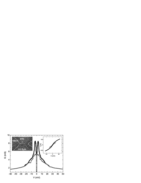
At 4.2 K junctions with widths down to 400 nm showed superconductivity with critical current densities of several A/cm2. The inset of Fig. 1 shows typical current-voltage characteristics (IVCs) of a nm2 junction. In the following we present two sets of transport and noise measurement of this GBJ referred to as 1st run and 2nd run. The full symbols represent the data obtained in the 1st run performed immediately after sample preparation. The open symbols show the result of the 2nd run performed after the sample has been stored in vacuum for a few days at room temperature. In both runs the junction clearly shows a hysteretic IVC with critical currents A and A, respectively. The differential conductance measured using standard lock-in technique is shown in Fig. 1. Both curves reveal a strong increase of with decreasing (the dip close to zero voltage is caused by the hysteretic IVC). This is in contrast to a decrease of expected for tunnel junctions below the gap voltageGross97 . After the vacuum storage both and at mV are noticeably reduced compared to the first run. This most likely is caused by oxygen loss close to the grain boundary during vacuum storage. For mV the curves are nearly identical. The fine structures in the spectra are reproducible features which have been observed for different samples up to 20 to 30 K, where they are continuously smeared out. Both the increase of below the gap voltage and the fine structure in the curves can be qualitatively understood in terms of the model of Blonder, Tinkham, and Klapwijk (BTK), assuming a grain boundary barrier with high transmissivityBlonder82 ; Klapwijk82 ; Loefwander99 . We note that GBJs with larger misorientation angles have barriers with smaller transmissivity resulting in tunneling like curvesGross97 ; Alff98a .
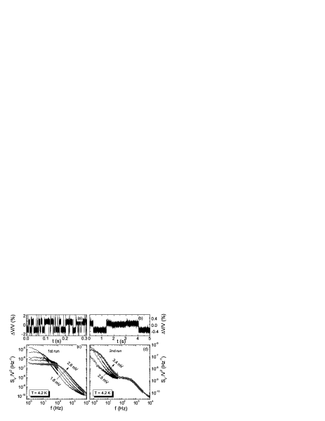
The voltage fluctuations were measured with a low- dc SQUID amplifierMarx95a . In Fig. 2 (c) and (d) two series of voltage noise spectra are shown which have been measured at 4.2 K for different junction voltages. Fig. 2 (a) and (b) display examples of time traces recorded at the same temperature for mV clearly showing distinct random telegraph switching (RTS) signals with relative switching amplitudes up to 3% in the 1st run and approximately 0.5% in the 2nd run. Assuming a homogeneous current density and a total suppression of the local conductance around the responsible noise centers these switching amplitudes correspond to an impact radius of 7.6 nm and nm, respectively. The two-level signals dominated of both runs up to K. However, the extremely large fluctuation observed in the 1st run could not be detected in the 2nd run. Together with a surface degradation of the sample we expect a loss or redistribution of oxygen at the grain boundary, leading to either a direct creation/destruction of noise centers or a current redistribution around them, to be the most likely explanation for this change of the noise properties between the two measurements.
Within the accessible frequency range (0.5 to 2104 Hz) all spectra could be well fitted with a superposition of a few () independent Lorentzian componentsMachlup54
| (1) |
together with a weak -background ( V2). Each Lorentzian component represents the contribution of a single two-level fluctuator (TLF) with a switching amplitude and mean lifetimes and in the upper and lower resistance state, respectively. From the fits to the spectra we obtained the effective lifetimes
| (2) |
as well as the mean squared fluctuation amplitudes
| (3) |
of the underlying RTS signals.
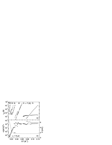
Fig. 3 shows the temperature dependence of and over a broad range of temperatures in an Arrhenius plot for a series of TLFs of a junction after the vacuum storage. The measurement was performed at a constant bias current of 10 A. All fluctuators show a thermally activated behavior in the temperature range from 8 to 80 K as has already been observed by Kemen et al.Kemen99 . By fitting an Arrhenius law to the data we found activation energies to 145 meV and attempt times to s typical for charge trapping centers in oxide materialsRogers85 . Applying a small magnetic field had no effect on the effective lifetimes and only minor effects on the mean squared switching amplitude even for . We therefore exclude magnetic flux jumps in the junction or adjacent film regions as the origin of the RTS signals as has been proposed for RTS noise in high thin films and SQUIDsJung91 .
The temperature dependence of as shown in Fig. 3 shows two striking features. Firstly, there is a crossover from an almost constant value below K to an exponential decrease for K. Secondly, the relative mean squared switching amplitudes of all fluctuators follow a common temperature dependence in spite of the broad scatter in the effective lifetimes without any systematic variation with temperature. This indicates that the population dynamics of a trap and its influence on the charge transport seem to be decoupled. The crossover temperature roughly corresponds to the temperature where the voltage at A starts to increase (dashed line in Fig. 3b). Since depends on both the relative switching amplitude and the ratio of the switching times (see Eq. (3)), it is hard to tell the reason for the exponential decrease in Fig. 3b because exponentially depends on both and (cf. Fig. 4). On the other hand, judging from the diverse temperature dependencies of the individual fluctuators in Fig. 3a and the fact that there were no more RTS signals resolvable over the apparently featureless noise background in the time traces at high temperatures, it is reasonable to conclude that the decrease of is to a large extent due to a decrease of the relative switching amplitude. It is further interesting to note that this decrease of would coincide with the decrease of the enhanced conductance in the low voltage regime which may be interpreted in a way that the noise centers in the junction mainly affect a distinct kind of conductance channels which are only active at low temperatures. Clearly, a detailed investigation of the and dependence of and is needed to clarify this issue.
The large RTS signal () which occurred during the first run allowed for a direct analysis of the voltage time traces. Thus the mean lifetimes and of both voltage states and the switching amplitude could be determined independently (this is not possible by analyzing the noise spectra without further assumptions, see Eqs. (2) and (3)). As the switching times in the two conductance states were found to be exponentially distributed at specific values of the voltage and temperature, the mean lifetimes could be determined by fitting an exponential decay function to the switching time histogram of the respective state.
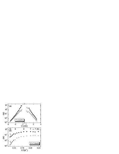
Fig. 4 shows the voltage and temperature dependence of the mean lifetimes in the upper and lower voltage state at K and mV. Both lifetimes decrease exponentially with the applied voltage at a similar rate. This confirms our previously reported results for the effective lifetimes which have been derived from Lorentzian fits to a series of noise spectra measured on a 1 m wide YBCO-GBJKemen99 . In addition to that our data show that the ratio of the switching times varies only weakly with the applied voltage and that they are almost independent of the bias direction. In terms of the trap model this indicates a symmetric position of the observed trap within the barrier regionRogers87a .
From Fig. 4b it becomes obvious that not only the effective mean lifetimes show a thermally activated behavior at K but that the lifetimes of both voltage states are thermally activated with different kinetic parameters both lying in the same range found for the effective lifetimes (see above). Furthermore, for K both switching times turn over to a independent behavior indicating a tunneling-like switching in this temperature range. These observations are in good agreement with our former results concerning the effective lifetimes at low temperaturesKemen99 .
In summary, we have fabricated submicron YBCO-GBJs with areas down to using electron beam lithography and measured their electrical transport and noise properties. The noise spectra and the voltage vs time traces were found to be dominated by random telegraph switching signals. The switching kinetics were found to be tunneling-like at K and thermally activated above this value up to . At low the mean lifetimes decrease exponentially with the junction voltage. These results confirm the assumption that the low frequency noise in high- GBJs is caused by the stochastic capture and release of charge carriers at trapping centers within the barrier region. In addition, we found a similar mean squared switching amplitude for all two-level fluctuators in a sample which follows a common temperature dependence decaying exponentially above about 30 K.
This work is supported by the Deutsche Forschungsgemeinschaft (Ma 1953/1-1).
References
- (1) R. Gross, L. Alff, A. Beck, O. M. Froehlich, D. Koelle, and A. Marx, IEEE Trans. Appl. Supercond. 7(2), 2929 (1997).
- (2) D. Koelle, R. Kleiner, F. Ludwig, E. Dantsker, and J. Clarke, Rev. Mod. Phys. 71(3), 631 (1999).
- (3) L. Alff, S. Kleefisch, U. Schoop, M. Zittartz, T. Kemen, T. Bauch, A. Marx, and R. Gross, Eur. Phys. J. B 5, 423 (1998).
- (4) M. Kawasaki, P. Chaudhari, and A. Gupta, Phys. Rev. Lett. 68(7), 1065 (1992).
- (5) T. Kemen, A. Marx, L. Alff, D. Koelle, and R. Gross, Trans. Appl. Supercond. 9, 3982 (1999).
- (6) A. Marx, L. Alff, and R. Gross, Appl. Supercond. 6(10–12), 621 (1999).
- (7) A. Marx and R. Gross, Appl. Phys. Lett. 70(1), 120 (1997).
- (8) A. Marx, L. Alff, and R. Gross, IEEE Trans. Appl. Supercond. 7(2), 2719 (1997).
- (9) A. Marx, U. Fath, L. Alff, and R. Gross, Appl. Phys. Lett. 67(13), 1929 (1995).
- (10) A. Marx, U. Fath, W. Ludwig, R. Gross, and T. Amrein, Phys. Rev. B 51(10), 6735 (1995).
- (11) L. Hao, J. C. Macfarlane, and C. M. Pegrum, Supercond. Sci Technol. 9, 678 (1996).
- (12) K. S. Ralls and R. A. Buhrman, Phys. Rev. B 44(11), 5800 (1991).
- (13) C. T. Rogers and R. A. Buhrman, Phys. Rev. Lett. 55(8), 859 (1985).
- (14) G. E. Blonder, M. Tinkham, and T. M. Klapwijk, Phys. Rev. B 25(7), 4515 (1982).
- (15) T. M. Klapwijk, G. E. Blonder, and M. Tinkham, Physica 109 & 110B, 1657 (1982).
- (16) T. Löfwander, G. Johansson, and G. Wendin, Current-voltage relations in -wave Josephson junctions:effects of midgap interface states (1999), cond-mat/9908261.
- (17) S. Machlup, J. Appl. Phys. 25(3), 341 (1954).
- (18) G. Jung, S. Vitale, and J. Konopka, J. Appl. Phys. 70(10), 5440 (1991).
- (19) C. T. Rogers, A Study of Individual Electron Trapping Centers and Noise in Metal-Insulator-Tunnel Junctions, Ph.D. thesis, Cornell University (1987).