Determination of the (33)-Sn/Ge(111) structure by photoelectron diffraction.
Abstract
The bonding geometry of Sn on Ge(111) has been quantitatively determined for the phase at 150 K. Energy scan photoelectron diffraction of the Sn 4d core levels has been used to independently measure the bond length between Sn and its nearest neighbour Ge atoms and the vertical distance between Sn and the Ge atom beneath. This latter distance is found to be 0.3 Å larger for one Sn atom out of the three contained in the lattice unit cell. The bond lengths and the bond directions, obtained by the angular scans, are found to be practically the same for the three Sn atoms within 0.03 Å and 3∘, respectively. The three nearest neighbour Ge atoms thus partially follow the Sn atom in its vertical ripple.
pacs:
PACS numbers: 61.14Qp, 79.60Dp, 68.35BsI Introduction
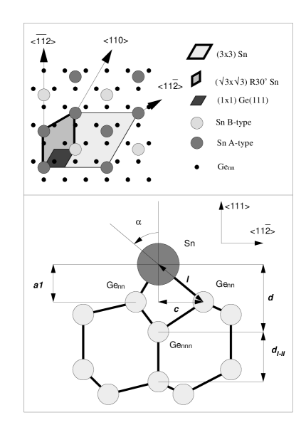
At a coverage of about 1/3 monolayer (ML), Sn and Pb deposited on Ge(111) below 550 K form a metastable R30∘ phase, where the Sn or Pb atoms occupy T4 sites above the Ge lattice. This phase continuously and reversibly transforms into a one, upon cooling below 200 K. This new phase was first observed by scanning tunneling microscopy (STM) on the Pb/Ge and Sn/Ge systems and attributed to the manifestation of a surface charge density wave (CDW).[1, 2, 3] The nature of this phase transition is still an open issue, also because of the controversal determination of the atomic structure of the two phases.[4, 5, 6] The low temperature phase is formed by three inequivalent Sn atoms per unit cell. X-ray diffraction (XRD) and low energy electron diffraction (LEED) experiments now consistently point to an atomic structure where one Sn atom out of three protrudes above the surface.[5, 7] A vertical ripple of 0.3 Å is thus observed between the Sn atoms of the surface unit cell. Within the CDW model the inequivalence between the Sn atoms should disappear in the room temperature (RT) phase. This is consistent with the most recent experiments that indicate equivalent Sn atoms at the same height level in the adatom layer at RT.[5, 7]
X-ray photoemission spectroscopy (XPS) experiments on the phase indeed show two Sn 4d core level doublets split by 0.4 eV, with an intensity ratio of approximately 2:1 between the two components (A and B, majority and minority components, respectively),[8, 9, 10] thus indicating two different kinds of Sn atoms. This spectrum remains practically unchanged throughout the phase transition.[8, 9, 11] This opens the way to alternative explanations, such as dynamical fluctuations[11] and order-disorder phase transitions,[9] where the local structure of the two phases is the same. Very recently the strong influence on the phase transition of small defect concentration has been put in evidence.[12, 13] Recently published XPS studies[14] suggest that, at exactly 1/3 ML coverage, the Sn 4d spectrum is different from that reported in the literature up to now. In particular the spectrum would show an intensity ratio between the A and B component appreciably different from that reported in previous works and would have an additional component in the high temperature phase. These findings were used to support the CDW model.
It is therefore important to determine the exact lineshape of the Sn spectrum and to measure the structure by XPS experiments on the single Sn core level components in order to check its consistency with that obtained by XRD and to identify the bonding sites of the atoms contributing to the majority and minority components. We have thus performed photoelectron diffraction (PED) measurements of the Sn 4d core levels at the ALOISA beamline (Elettra Synchrotron). The wide variety of scattering geometries accessible at the ALOISA end station allowed us to measure separately the bond direction and length between the Sn adatom and its three nearest neighbour Ge atoms (Genn) and the Sn vertical distance to the next nearest neighbour Ge atom beneath (Gennn). In a previous paper we qualitatively reported on the preliminary experimental results, i.e. the substantial equivalence of the Sn–Genn bond angle and length for both A and B type Sn atoms, which mainly differ for their vertical height Sn–Gennn.[15] Here we present the quantitative determination of the bonding geometry of Sn atoms in the unit cell, as obtained by fitting to multiple scattering calculations (MSCD)[16] the PED data obtained in a more extended energy range and with a better statistics. We attribute each of the two components of the Sn 4d photoemission spectrum to a specific bonding geometry of the two inequivalent types of Sn atoms. To our knowledge, such a direct correlation was never extracted before. The rippled structure obtained in the present work is in good agreement both with previous XRD determinations[5, 7] and with recent density functional calculations (DFT) performed in the local density approximation with gradient correction (LDA-GC)[17] and in combination with local-orbital (LDA-LO) methods[18].
II Experimental set-up and sample preparation
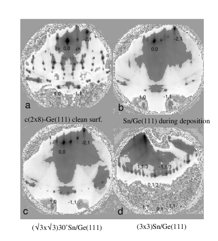
The present experiment has been performed in the UHV end station of the ALOISA beamline[19, 20] at the Elettra synchrotron (Trieste). Details about the experimental setup and sample cleaning are given elsewhere.[15] We have used a Reflection High Energy Electron Diffraction (RHEED) system to monitor in real time the preparation of the -phase of Sn on Ge(111). We have followed a procedure slightly different from the standard one reported in the literature. Sn is usually evaporated on samples held at RT and successively annealed to T 500 K. In this conditions, only a diffuse diffraction pattern is observed during deposition and the surface quality can be only judged a posteriori. Therefore the same surface coverage may not be easily reproduced, being subject to any unstability of the evaporation cell. By He atom scattering (HAS) experiments with high angular resolution, we have seen that the best surface quality (i.e. narrowest diffraction peaks of both the and phases) is obtained when depositing on the surface kept close to 500 K.[21] At the ALOISA end-station we have used the RHEED system (which is a long range order probe similar to HAS) to monitor the diffraction pattern along the surface direction while depositing at T 500 K. The spots soon disappear leaving only a streaky pattern.[22] After 2/3 of the total exposure used in our work, the spots of the start to appear (see panel of Fig. 1), but the deposition is just stopped when the half-integer streaky peaks disappear (see panel of Fig. 1). The surface is shortly flashed at about 530 K and then cooled down. Higher flashing temperature irreversibly leads to a stable phase, as previously reported [23]. Shorter exposures never lead to the complete disappearance of the pattern. After this procedure sharp spots of the R30∘ phase are observed along the direction. To detect the spots characteristic of the phase, the RHEED pattern was observed along the direction, as shown in the panel of Fig. 1, which is taken at T 150 K. We have seen that no degradation of the photoemission spectra nor of the RHEED patterns occurs for at least 10 hours, when the sample is left inside the experimental chamber. In any case, a new surface was always prepared after 10 hours.
The whole set of spectroscopical data hereafter shown has been taken with constant electron energy resolution of 170 meV. The photon energy resolution has been always meV. The overall instrumental resolution is thus meV.
III Results and Discussion
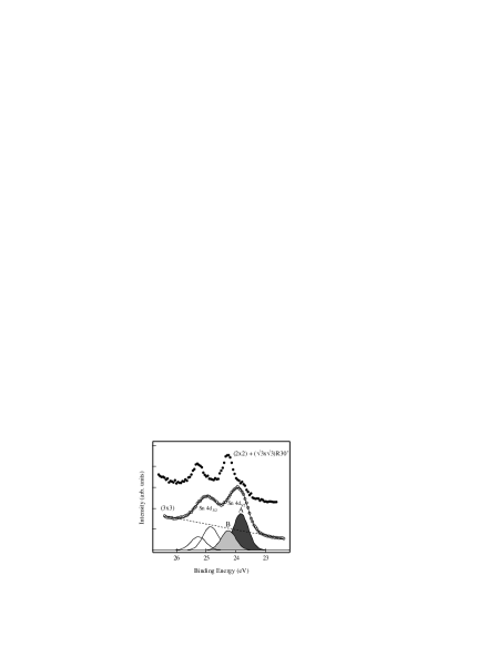
Fig. 2 shows a typical Sn photoemission spectrum taken at eV photon energy on the phase. In agreement with previous observations,[8, 9, 10, 11] but in contrast with the results presented by Kidd et al.,[14] it can be fitted to two spin-orbit split doublets, shifted by eV and with an intensity ratio close to 2:1. Any deviation from this shape was always associated to residual or phases as observed by RHEED patterns. A spectrum taken at a deposition stage close to that shown in the panel of Fig. 1 can also be seen in Fig. 2. This spectrum shows a peak at 24.3 eV binding energy, which is characteristic of the phase. This observation is fully consistent with the previous measurements reported in the literature.[8, 10, 11] The experiments have been performed by taking the whole Sn 4d spectrum for each point of the PED angular and photon energy scans at T K. Four gaussians have been used to fit the spectra, while both the spin-orbit splitting of the doublets and the energy splitting between the A and B components were kept fixed. The same full width at half maximum has been used for all the components. A low order polinomial () has been used for background subtraction. The PED data points shown in the present analysis represent the so called -function,[24] , where is the integrated intensity of the component of the A or B type Sn atoms. is a smoothly varying background of , modulating both the angular and energy PED features. essentially takes into account the energy dependence of the atomic photoionization cross-section and the angular dependence of the polarization and of the illuminated sample area. has been evaluated by a low order () polynomial fitting of .
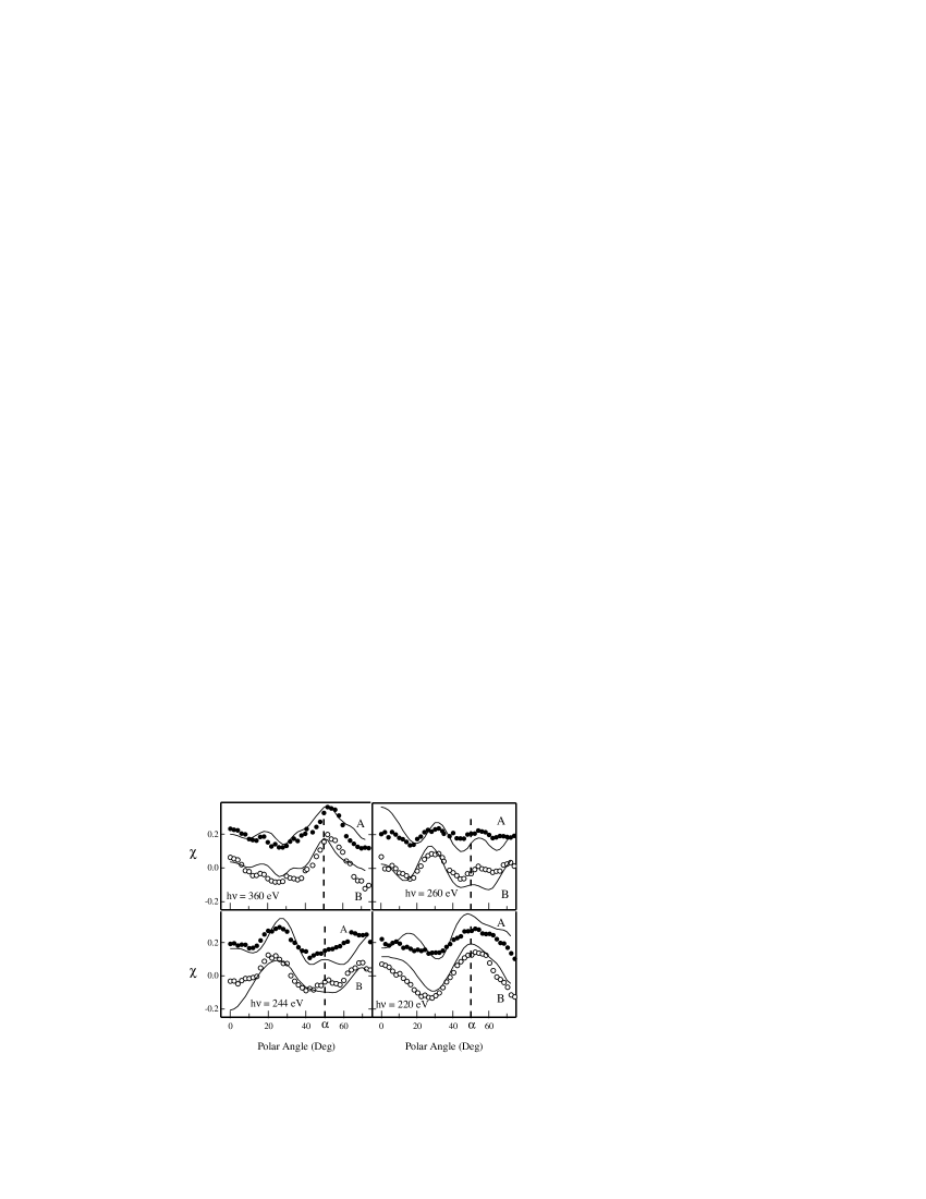
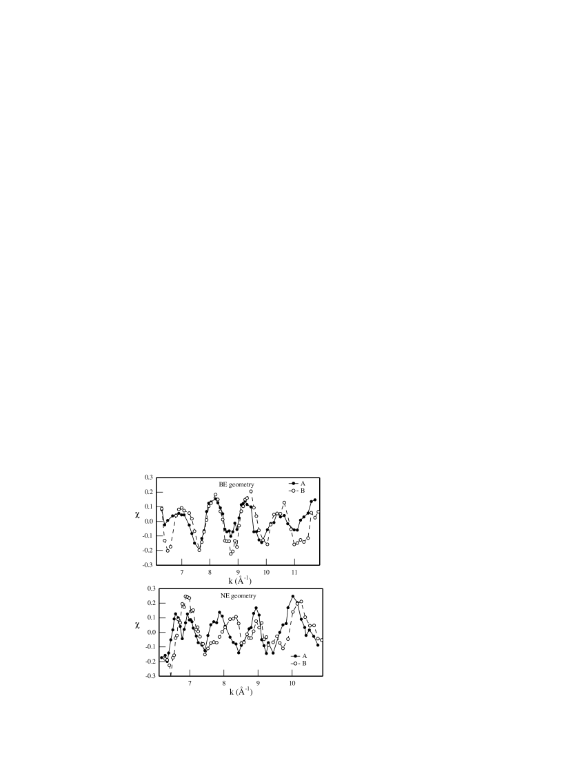
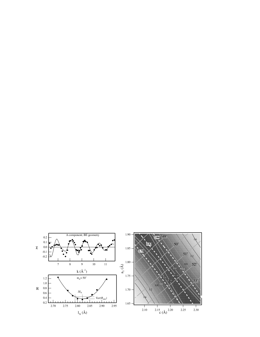
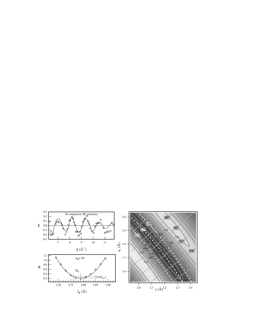
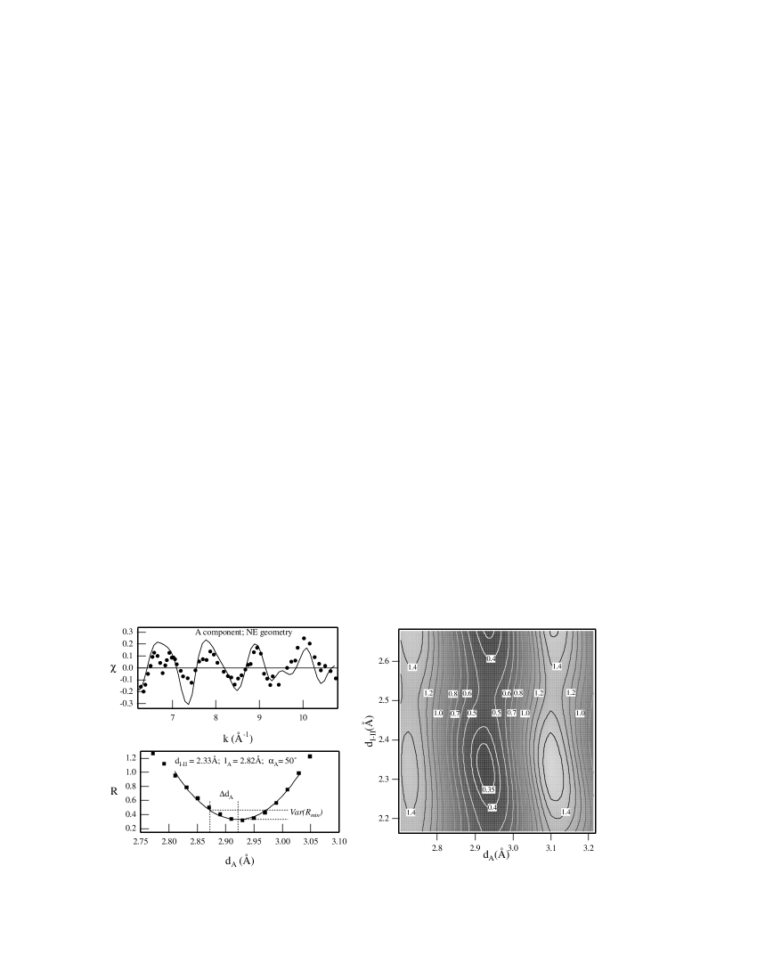
First we have measured the polar scans from the surface normal (normal emission, NE, conditions) to the horizon (grazing emission) for six different photon energies and the three inequivalent main symmetry directions of the surface. The scans have been performed by keeping the sample in transverse-magnetic () polarization, i.e. with the scattering plane normal to the magnetic field of the photon beam, and rotating the analyzer in the scattering plane. When the surface is oriented with the [2] direction in the scattering plane, at a specific angle from the surface normal the analyzer is aligned with the Sn-Genn bond angle (see Fig. 3). In this, so called, bond emission (BE) geometry, the Sn photoelectrons can be efficiently backscattered by the Genn atom and give rise to intensity maxima and minima, when changing the photon energy. By a simple visual inspection, the bond direction for both A and B Sn atoms can be roughly estimated as 50∘ from the surface normal (see the polar scans taken at 360 and 220 eV in Fig. 4). Given the information on the bond direction, the bond length has been determined by variable energy PED scans in BE geometry. The polarization vector of the photon beam has been oriented at 50∘ from the surface normal, along the bond direction. This choice enhances the sensitivity to the Sn-Genn bond length, as shown by MSCD simulations.[15] A very similar photon energy dependence has been found for both A and B components in BE condition (see upper panel of Fig. 5).[15] Finally, the Sn height above the underneath Gennn atom has been measured by taking energy scans in NE conditions and with the sample surface in polarization. In this case the A and B components display a remarkably different energy dependence, as can be seen in the lower panel of Fig. 5.
The quantitative evaluation of , and for both A and B type of Sn atoms has been performed by fitting the data to the MSCD simulations, starting from the geometric structure recently obtained by LDA-GC calculations.[17] The simulations have been performed on a 30 atom cluster centered on the Sn atom by considering multiple scattering up to the 8th order, 4th Rehr-Albers order and with a pathcut of 1.[16] Lower pathcut values did not modify the simulations appreciably. A Debye temperature of 230 K and an inner potential eV have been obtained by fitting the energy scans and successively they have been kept fixed in the recursive fitting procedure.
The fit quality has been evaluated by means of the commonly used reliability factor . In order to compare our results with previously published structural studies, the random error has been estimated following the approach of Woodruff and Bradshaw for the analysis of the variable energy PED.[25] By applying the method described by Pendry for LEED,[26] the variance of the R-factor is calculated for its minimum value. The variance is evaluated as , where is the number of independent pieces of structural information within the spectrum energy range.[25] All the parameter values yielding structures with associated R-factor lower than are regarded as falling within one standard deviation from that of the best fit structure. Assuming a parabolic form of the R-factor, the random error on the parameter is evaluated as
| (1) |
where the other parameters () are taken at the minimum of the R-factor. As a result an error of and Å has been found for and , respectively. Due to the intrinsic limit of this approach, that assumes the structural parameters to be independent, we have also checked, by visual inspection, that a deviation of 0.05 Å from the best fit value produces significative differences in the simulation curve.
Due to computational limits, the BE and NE energy scans have been independently fitted. However, they are essentially sensitive to a single parameter ( and , respectively). The preliminary results for and , obtained by comparing data and simulations by visual inspection, have then been used to fit all the polar scans at the same time in order to obtain the bond angle . The new value for has then been used to obtain better and values from the R-factor analysis of the energy scans. This fitting procedure has been iterated until a self-consistent evaluation of , and was obtained for both A and B components from the entire set of PED data.
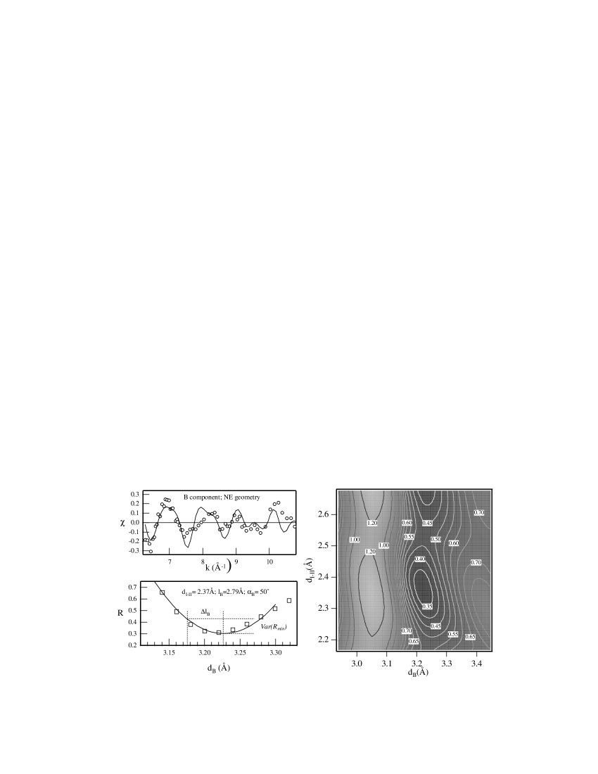
The refined bond length and its error have been found from the BE data by calculating the reliability R-factor for grid simulations on two parameters, and (, see Fig. 3) with the other parameters fixed at their best fit value. As can be seen in Figs. 6 and 7, a well defined minimum is obtained for Å and Å, while an uncertainty of almost 10∘ is given for the bond direction. We have also observed that, in BE conditions, the simulation is weakly affected by the position of the surrounding next nearest neighbour Ge atoms (not even by the Gennn underneath the Sn atom).
In the case of the NE scan, the grid scan simulations have been performed spanning over the Sn-Gennn distance and the distance between the first and second Ge bi-layers. As shown in Figs. 8 and 9, the R-factor analysis yields two different heights, Å and Å, for the A (majority) and B (minority) type Sn atoms. It must be emphasized that the cluster used for the simulations contains one Sn atom only. The relative height between the A and B clusters is thus undetermined, but the difference of Å is in good agreement with the calculated[17, 18] and measured[5, 7] vertical ripple of the adatom layer. For what concerns other structural parameters, the NE scans have been found weakly sensitive to . From a comparison with the polar scan simulations, has been estimated to be 0.05-0.1 Å shorter than the Ge bulk interlayer separation, for both A and B type Sn atoms.
The polar scans are sensitive to the whole atomic environment of the Sn atom (particularly to the bond angle ), but they display much less features with respect to the energy scan (see Fig. 4). The angular patterns have thus been fitted to check the consistency of the overall structure, as obtained by the NE and BE scans. The same bond angle has been determined for both A and B type Sn atoms, with an uncertainty of .
The parameters obtained from the analysis of the whole PED data set are shown in Table I and compared to the calculated[17, 18] and previously measured[5, 7] values. There is a qualitative agreement concerning the overall picture. In particular, the nearest neighbour Genn atoms nearly follow the Sn atom in its vertical displacement. According to our data, the three nearest neighbour Genn atoms have the same bond length and direction for both A and B type Sn atom, within Å and respectively. This is also consistent with the ripple of the Ge atoms of the first layer as reported in the literature ( Å).[5, 7, 17, 18] The most recent DFT calculations[17, 18] are in agreement with our results, particularly for what concerns the vertical height . Small discrepancies are only obtained for the Sn-Genn bond angle, which, on the other hand, yields the higher uncertainty in our measurements. Therefore the PED of the two components of the Sn spectrum, characteristic of the phase,[9, 11] yields a vertically distorted structure, consistently with the XRD[5] and XRD/LEED[7] determinations. The component with the highest binding energy (minority B) is associated to the Sn atoms that protrude above the surface.
IV Conclusions
By comparing the RHEED patterns and the photoemission spectra we have checked that the correct lineshape of the Sn spectrum on the phase is similar to that reported in several articles.[8, 9, 10, 11] In addition, the lineshape, recently proposed by Kidd et al. for the phase,[14] has been only observed when residual phase was present. We have determined the structure of the low temperature -Sn/Ge(111) phase by means of photoelectron diffraction from the Sn core levels. The PED measurements and analysis have been performed on a set of photoemission spectra, which can be always fitted to two components. Exploiting the scattering geometry of the experimental apparatus, we have separately measured the Sn-Genn bond parameters and the vertical height of Sn above the underneath Gennn atom for the two kind of Sn adatoms. The results are consistent with the most recent XRD measurements[5] and theoretical predictions[17, 18], where one Sn atom out of three is vertically displaced by Å. This vertical ripple is strongly coupled to the distortion of the first Ge bi-layer. In particular, the tetrahedron formed by the Sn atom and its three nearest neighbours Genn atoms is found to retain the same structure for both A and B components within the experimental error. The vertical height above the Gennn atom is the main difference between the two bonding geometries. The Sn atoms that protrude out of the surface have the highest binding energy (minority component), while the majority A component (lowest binding energy) is associated to the Sn atoms that are pushed closer to the Ge(111) surface.
V acknowledgements
We are grateful to M.A. Van Hove and Y. Chen for providing the MSCD package for PED analysis. We thank E. Tosatti for useful discussions. This research has been partially funded by MURST cofin99 (Prot. 9902332155), by Regione Friuli-Venezia Giulia 98 and by INFM-PAIS F99. M.B. acknowledges a grant by MURST cofin99 (Prot. 9902112831).
Added note: meanwhile the present paper was being refereed, a photoemission and LEED study was published, showing the correlation between the Sn line shape and the (33)-Sn/Ge(111) phase, in full agreement with our analysis.[27]
REFERENCES
- [1] J.M. Carpinelli, H.H. Weitering, E.W. Plummer, and R. Stumpf, Nature 381, 398 (1996).
- [2] J.M. Carpinelli, H.H. Weitering, M. Bartkowiak, R. Stumpf, and E.W. Plummer, Phys. Rev. Lett. 79, 2859 (1997).
- [3] S. Scandolo, F. Ancilotto, G.L. Chiarotti, G. Santoro, S. Serra, and E. Tosatti, Surf. Sci. 402-404, 808 (1998).
- [4] A.P. Baddorf, J. Jahns, J. Zhang, J.M. Carpinelli, and E.W. Plummer, Phys. Rev. B 57, 4579 (1998).
- [5] O. Bunk, J.H. Zeysing, G. Falkenberg, R.L. Johnson, M. Nielsen, M.M. Nielsen, and R. Feidenhans’l, Phys. Rev. Lett. 83, 2226 (1999).
- [6] A. Mascaraque, J. Avila, J. Alvarez, M.C. Asensio, S. Ferrer, and A.G. Michel, Phys. Rev. Lett. 82, 2524 (1999).
- [7] J. Zhang, Ismail, P.J. Rous, A.P. Baddorf, and E.W. Plummer, Phys. Rev. B 60, 2860 (1999).
- [8] G. Le Lay, V. Yu. Aristov, O. Boström, J.M. Layet, M.C. Asensio, J. Avila, Y. Huttel, A. Cricenti, App. Surf. Sci. 123/124, 440 (1998).
- [9] R.I.G. Uhrberg and T. Balasubramanian, Phys. Rev. Lett. 81, 2108 (1998).
- [10] J. Avila, Y. Huttel, A. Mascaraque, G. LeLay, E.G. Michel, and M.C. Asensio, Surf. Sci. 433-435, 327 (1999).
- [11] J. Avila, A. Mascaraque, E.G. Michel, M.C. Asensio, G. Le Lay, J. Ortega, R. Pérez, and F. Flores, Phys. Rev. Lett. 82, 442 (1999).
- [12] A.V. Melechko, J. Braun, H.H. Weitering, and E.W. Plummer, Phys. Rev. Lett. 83, 999 (1999); ibidem Phys. Rev. B 61, 2235 (2000).
- [13] H.H. Weitering, J.M. Carpinelli, A.V. Melechko, J. Zhang, M. Bartkowiak, and E.W. Plummer, Science 285, 2107 (1999).
- [14] T.E. Kidd, T. Miller, and T.-C. Chiang, Phys. Rev. Lett. 83, 2789 (1999).
- [15] L. Floreano, L. Petaccia, M. Benes, D. Cvetko, A. Goldoni, R. Gotter. L. Grill, A. Morgante, A. Verdini, and S. Modesti, Surf. Rev. Lett. 6, 1091 (1999).
- [16] Y. Chen, F.J. Garcia de Albajo, A. Chasse, R.X. Ynzunza, A.P. Kaduwela, M.A. Van Hove, and C.S. Fadley, Phys. Rev. B 58, 13121 (1998); the MSCD program package is available at the web address: “http://electron.lbl.gov/mscdpack/mscdpack.html”.
- [17] S. de Gironcoli, S. Scandolo, G. Ballabio, G. Santoro and E. Tosatti, Surf. Sci. 454-456, 172 (2000).
- [18] J. Ortega, R. Perez, and F. Flores, J. Phys. Condens. Matter 12, L21 (2000).
- [19] L. Floreano, G. Naletto, D. Cvetko, R. Gotter, M. Malvezzi, L. Marassi, A. Morgante, A. Santaniello, A. Verdini, F. Tommasini and G. Tondello, Rev. Sci. Instrum. 70, 3855 (1999).
- [20] Further details can be found at the web address “http://tasc.area.trieste.it/tasc/lds/aloisa/aloisa.html”.
- [21] L. Floreano, D. Cvetko, G. Bavdek and A. Morgante, Phys. Rev. B, in press (http://arxiv.org/archive/cond-mat/0011236).
- [22] S.B. DiCenzo, P.A. Bennett, D. Tribula, P. Thiry, G.K. Wertheim, and J.E. Rowe, Phys. Rev. B 31, 2330 (1985).
- [23] T. Ichikawa and S. Ino, Surf. Sci. 105, 394 (1981).
- [24] D.P. Woodruff and A.M. Bradshaw, Rep. Prog. Phys. 57, 1029 (1994).
- [25] N.A. Booth, R. Davis, R. Toomes, D.P. Woodruff, C. Hirschmugl, K.M. Schindler, O. Schaff, V. Fernandez, A. Theobald, Ph. Hofmann, R. Lindsay, T. Gießel, P. Baumgärtel, and A.M. Bradshaw, Surf. Sci. 387, 152 (1997).
- [26] J.B. Pendry, J. Phys. C, Solid State Phys. 13, 937 (1980).
- [27] R.I.G. Uhrberg, H.M. Zhang, and T. Balasubramanian, Phys. Rev. Lett. 85, 1036 (2000).
| Parameter | SXRD[5] | SXRD/LEED[7] | LDA-LO[18] | LDA-GC[17] | Present paper |
|---|---|---|---|---|---|
| 50∘ | 51.5∘ | 51.8∘ | 51.2∘ | 50∘ | |
| 47.4∘ | 46.9∘ | 49∘ | 47∘ | 50∘ | |
| 2.80 | 2.89 | 2.78 | 2.79 | 2.82 | |
| 2.88 | 2.93 | 2.79 | 2.84 | 2.79 | |
| 3.03 | 2.97 | 2.90 | 2.92 | 2.92 | |
| 3.32 | 3.34 | 3.13 | 3.25 | 3.23 | |
| 2.36-2.39 | 2.39 | 2.31-2.36 | 2.34-2.39 | 2.34-2.40 | |
| 0.29 | 0.37 | 0.23 | 0.33 | 0.31 |