[
Dephasing and Metal-Insulator Transition
Abstract
The metal-insulator transition (MIT) observed in two-dimensional (2D) systems is apparently contradictory to the well known scaling theory of localization. By investigating the conductance of disordered one-dimensional systems with a finite phase coherence length, we show that by changing the phase coherence length or the localization length, it is possible to observe the transition from insulator-like behavior to metal-like behavior, and the transition is a crossover between the quantum and classical regimes. The resemblance between our calculated results and the experimental findings of 2D MIT suggests that the observed metallic phase could be the result of a finite dephasing rate.
pacs:
PACS numbers: 71.30.+h, 73.40.Hm] Since the discovery of the metal-insulator transition in two-dimensional (2D) systems[1], several theoretical models have been proposed to understand the phenomena. Among the proposed theories, some[2, 3, 4, 5] can be considered as semi-classical theory. Although they are different in details, the basic idea is the same. They all consider that the metallic phase observed in the experiments is the classical phase, i.e., the metallic behavior of the system can be well understood under the classical picture. For instance, the percolation model, initially proposed by He and Xie[2] and further extended by Meir[5], provides good description of many experimental facts. In this approach, the system consists of inhomogeneous carrier distribution with high density conducting regions and low density insulating regions. By assuming that the electrons are totally dephased in each separate region, one can consider the metal-insulator transition as the classical percolation transition of the high density conducting regions, and calculate the total conductance of the system by classical random resistance network. The dephasing of the carriers is essential for the model since a pure quantum system will never percolate according to the well-known scaling theory of localization[6].
It is not obvious that a system can be considered as a classical system at low temperatures. A recent experiment [7] on 2D systems shows that the phase coherence length is quite long, typically 600-1000 nm. Thus, it is more likely that a real system is in the regime where quantum effects compete with classical effects. Classical effects are manifested by a finite phase coherence length, which may be due to a finite temperature or other novel mechanisms. For instance, there are experimental indications that the dephasing rate may be finite even at zero temperature [8]. On the other hand, in a disordered 2D system, the quantum effect always causes the localization length to be finite. For a 2D system with metal-insulator transition, the localization length strongly depends on the carrier density. Actually, by changing the carrier density, the conductance of the system may change several orders [1] which implies a substantial change in the localization length. The behavior of the system is determined by two competing length scales: localization length and phase coherence length. Therefore, it is important to study transport properties by varying these two lengths.

In this paper, we study the interplay of disorder and dephasing of one-dimensional (1D) systems in transport properties. We limit to 1D models to reduce the severe finite-size effect in numerical results for higher dimensions, although our conclusion can be carried over to higher dimensions. Our 1D model (Fig.1) consists of normal random scatters and dephasing scatters, alternatively. While the normal random scatters give rise to a finite localization length, the dephasing scatters randomize electron phase. The normal random scatters are constructed by -barriers with random height , which has the distribution
In the model controls the randomness of the system. The transmission and reflection coefficients for the normal random scatters can be calculated from the transfer-matrix for individual -barrier [9],
where and are the transmission and reflection amplitudes for the barrier, and is the momentum of the injected electron. The transfer matrix for sequential -barriers can be calculated from
where is the transfer matrix describing the propagation of the electron from one -barrier to the next. Assuming the spacing between the neighboring barriers is unity, is
Using the transfer-matrix technique, the localization length can be determined analytically [9].
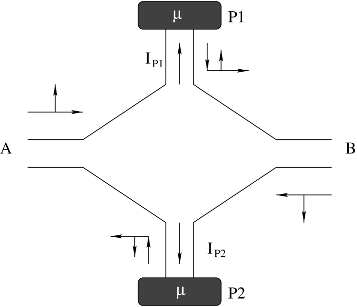
To introduce the dephasing effect into the system, one has to include the interaction between the system and the environment. The Büttiker model [10] shown in Fig.2 is the simplest way to achieve that. In this approach, the system is connected to the external electron reservoirs via the dephasing scatters. With a certain possibility, an electron is scattered into the external reservoirs, totally losing its phase memory, and then re-injected into the system. Two restrictions are imposed to reflect physical reality. First, the net current between the system and the reservoirs should be zero so that each scattered electron will finally return to the system. To do so, one can adjust the chemical potential of the external reservoirs such that where () is the current between the system and the external reservoir P1 (P2). Second, the system is connected to two identical electron reservoirs P1 and P2, and the -matrix between the system and the reservoirs is designed so that the electron is only scattered forward, thus the dephasing scatters will not cause any momentum relaxation. The -matrix reads [10]
where is the possibility that the electron is scattered to the reservoirs, namely, the dephasing rate. The phase coherence length is estimated by .
The localization length of the system is determined by the normal random scatters, while the phase coherence length is determined by the dephasing scatters. For a system with dephasing scatters, there are external chemical potentials with , where is the chemical potential for the left (right) measurement electrode. The system satisfies the multi-lead Ohm’s law,
The conductance between the leads, , is determined by the Landaur-Büttiker formula,
where is the transmission coefficient between the leads. For the leads attached to the dephasing scatters, the transmission coefficient is the sum of all transmission coefficients between leads P1 and P2,
The gauge invariance, namely shifting each by a constant should not affect the result, is satisfied through the condition
The total conductance of the system is calculated by imposing the condition
After some algebra, the total conductance of the system can be written as
Although we start from a seemly artificial model, the total conductance formula actually reflects physical reality. It contains two kinds of contributions: the first is the direct conductance coming from direct quantum tunneling; the second is the correction due to the dephasing effect caused by classical sequential tunneling. Thus, the conductance formula is consistent with the general picture of the dephasing effect on a conductance.
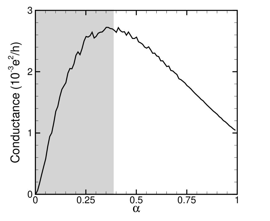
The typical behavior of the conductance for the system is shown in Fig.3, where we plot the conductance as a function of the dephasing rate . In a real system, the dephasing rate is a monotonic function of temperature, so the plot can also be considered as the temperature dependence of the conductance. We have systematically calculated the conductance for different sets of parameters, and the results show qualitatively similar behavior, although the peak position depends on the parameters. The most important feature of the plot is that the conductance is not a monotonic function of the dephasing rate, or temperature. The plot can be divided into two regions, the gray and white regions. In the gray region, the dephasing rate is low and the phase coherence length is long. The electron is localized within the phase coherence length, so the system shows quantum localization with insulator-like behavior, namely, the conductance decreases as temperature drops. This region can be considered as the quantum region. On the other hand, when the dephasing rate becomes higher, the system enters into the classical regime and the conductance increases with decreasing temperature, a typical metallic behavior.

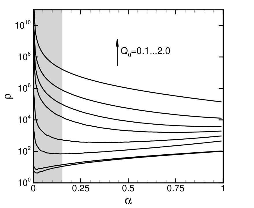
The turning point between the quantum and classical regimes can be determined by comparing the phase coherence length with the localization length calculated from the transfer matrix formalism [9]. The result is shown in Fig.4. The phase coherence length is obtained by using the value of corresponding to the peak in the conductance plot (see Fig.3) for a given . One can see that the two lengths are approximately equal. Thus, it shows that the transition occurs at the point where . From Fig.3 and Fig.4, one can clearly see that by changing the phase coherence length or the localization length, it is possible to observe the transition from the metal-like behavior to the insulator-like behavior, and the behavior of the system is determined by the competition between the localization length and the phase coherence length. When , the quantum physics of localizaiton ceases to exist. Therefore, we believe that it is the transition between the quantum and the classical phases.

Great resemblance can be found when comparing the experimental findings[1] with the results from this simplified model. In Fig.5 we plot the dephasing rate (or temperature) dependence of the resistance. Different curves are for different scattering parameter . Changing the carrier density is equivalent to changing the Fermi momentum, which in turn changes . Thus, different curves correspond to different carrier densities. In the plot, we impose a finite cutoff of the dephasing rate , which makes lower inaccessible (gray region in the plot). For above the cutoff, the phase coherence length is always finite. Depending on whether is larger or smaller than the localization length , one can either observe the metal-like or the insulator-like behavior, as shown in Fig.5. When the finite cutoff falls upon the turning point (the maximum conductance point in Fig.3), the system shows the “critical” behavior, where the resistance is nearly flat within a certain temperature range. In Fig.6, we show the density dependence of the conductance for different (or temperature). One can identify a “fixed” point where different curves cross at. Similar feature has been seen in many experimental plots.
The finite cutoff of the dephasing rate can be justified by two possible reasons. First, the cutoff may be due to a finite temperature. In this case, if we assume the dephasing rate goes to zero when temperature approaches zero, as suggested by a simple power law , there is always an upturn of the resistance at low enough temperature as shown in Fig.5 for low values of . This suggests a re-entrance to an insulator at low temperatures. The re-entry behavior may have already been observed in the recent experiment[11]. Under the circumstance, the transition is a finite temperature effect. The second possibility is that the dephasing rate might be finite at zero temperature[8]. Consequently, the metallic phase will survive even at zero temperature. If we adhere to the original definition that a metal has a finite resistance at zero temperature while the resistance of an insulator diverges, the system will always be a metal. The reason is that on the low density ”insulator” side, the resistance will saturate to a finite value at because of the finite phase coherence length. However, in a similar plot as shown in Fig.6, a ”fixed” point can still be identified which can be used as an operational definition of ”metal-insulator transition”.
The saturation of the dephasing rate at low temperatures is still a controversial issue. Some argue that the saturation observed in the experiments is not an intrinsic effect. Nevertheless, whether it is intrinsic or extrinsic, the same factors which cause the saturation should have a similar effect on the conductance. To justify a real metal-insulator transition, one has to clearly rule out those external factors that may cause finite dephasing rate at low temperatures [8].
In summary, we have studied the interplay between dephasing and disorder. Based on a 1D model, we show that by changing the phase coherence length or the localization length, it is possible to observe the transition from the insulator-like behavior to the metal-like behavior, which corresponds to a transition between quantum and classical phases. The great resemblance between the results from this simplified model and the experiments suggests that the quantum effect is important at low temperatures, although the high temperature behavior is dominated by the classical effect. We suggest that conductance experiment should be accompanied by a dephasing rate measurement to address the effect of a finite coherence length. Although our calculation is for a 1D model, the same physics should survive at higher dimensions.
The work is supported by DOE.
REFERENCES
- [1] S. V. Kravchenko et. al., Phys. Rev. B 51, 7038 (1995); S. V. Kravchenko et. al., Phys. Rev. Lett. 77, 4938 (1996).
- [2] Song He and X. C. Xie, Phys. Rev. Lett. 80, 3324 (1998); Junren Shi, Song He and X. C. Xie, Phys. Rev. B 60, R13950 (1999); Junren Shi, Song He and X. C. Xie, cond-mat/9904393.
- [3] S. Das Sarma and E. H. Hwang, Phys. Rev. Lett. 83, 164 (1999).
- [4] B. L. Altshuler and D. L. Malsov, Phys. Rev. Lett. 82, 145 (1999); B. L. Altshuler and D. L. Malsov, Phys. Rev. Lett. 83, 2092 (1999).
- [5] Y. Meir, Phys. Rev. Lett. 83, 3506 (1999).
- [6] E. Abrahams, P. W. Anderson, D. C. Licciardello and T. V. Ramakrishnan, Phys. Rev. Lett. 42, 673 (1979).
- [7] G. Brunthaler, A. Prinz, G. Bauer, V. M. Pudalov, E. M. Dizhur, J. Jaroszynski, P.Gold and T. Dietl, preprint cond-mat/9911011.
- [8] P. Mohanty, E. M. Q. Jariwala, R. A. Webb, Phys. Rev. Lett. 78, 3366 (1997); P. Mohanty and R. A. Webb, Phys. Rev. B 55, R13452 (1997).
- [9] B. S. Andereck, and E. Abrahams, Physics in One Dimension, edited by J. Bernasconi and T. Schneider (Springer-Verlag, 1981).
- [10] M. Büttiker, Phys. Rev. B 33, 3020 (1986) and references therein; S. Datta, Electronic Transport in Mesoscopic Systems (Cambridge University Press, 1995).
- [11] M. Y. Simmons, A. R. Hamilton, M. Pepper, E. H. Linfield, P. D. Rose and D. A. Ritchie, Phys. Rev. Lett. 84, 2489 (2000).