Voltage-flux-characteristics of asymmetric dc SQUIDs
Abstract
We present a detailed analysis of voltage-flux -characteristics for asymmetric dc SQUIDs with various kinds of asymmetries. For finite asymmetry in the critical currents of the two Josephson junctions, the minima in the -characteristics for bias currents of opposite polarity are shifted along the flux axis by relative to each other; is the screening parameter. This simple relation allows the determination of in our experiments on dc SQUIDs and comparison with theory. Extensive numerical simulations within a wide range of and noise parameter reveal a systematic dependence of the transfer function on and (junction resistance asymmetry) . As for the symmetric dc SQUID, factorizes into , where now also depends on . For we find mostly a decrease of with increasing , which however can only partially account for the frequently observed discrepancy in between theory and experiment for high- dc SQUIDs.
Index Terms:
High-temperature superconductors, SQUIDs, superconducting devices.I Introduction
The observation of a significant discrepancy between numerical simulations and experimental results obtained for direct current (dc) superconducting quantum interference devices (SQUIDs) based on high-transition-temperature superconductors (HTS) is one of the most important unsolved problems for HTS dc SQUIDs which seriously hinders their optimization for applications [1]. HTS dc SQUIDs show frequently asymmetric behavior which may be attributed to the large spread in the critical current and normal resistance of HTS Josephson junctions. This may lead to asymmetric critical current or voltage vs. external flux characteristics of the dc SQUID [2, 3] and can affect the transfer function which is defined as the maximum slope of the -curves. However, such an asymmetry has been usually neglected in numerical simulations of for HTS dc SQUIDs.
In this paper we present a detailed study of the impact of asymmetry on the -characteristics and in particular on the transfer function of dc SQUIDs. We first introduce the main parameters which define the asymmetric dc SQUID (Sec.II). Then we show that an asymmetry in of the two Josephson junctions leads to a shift of the - and in the -characteristics, which can be used to determine the critical current asymmetry experimentally, as demonstrated on dc SQUIDs with (YBCO) bicrystal grain boundary Josephson junctions [4] (Sec.III). We present numerical simulation results for which we obtained within a wide range of parameters including the limit of large thermal fluctuations which are important for HTS dc SQUIDs (Sec.IV), and we compare those results with experimental data on HTS dc SQUIDs (Sec.V).
II asymmetric dc SQUID
The asymmetric dc SQUID shown in Fig.1 consists of a superconducting loop of inductance intersected by two Josephson junctions with average values of critical current , resistance and capacitance .
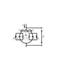
The asymmetry in the junction parameters is described via the asymmetry parameters , and , wich are defined according to
| (1) |
where the subscripts 1,2 denote the parameters of the left and right junction, respectively.
Throughout this paper we consider two different origins of the junction asymmetry, noting, that in real devices we may have a combination of both: (i) geometric asymmetry and (ii) intrinsic asymmetry.
In the case of geometric asymmetry we assume identical values of critical current density , resistance times area , and specific capacitance for both junctions. Here, is the junction area with width and length . We then introduce an asymmetry via different values for , assuming constant . In the case of bicrystal grain boundary junctions equals the film thickness , which can be assumed to be constant in practical devices. The geometric asymmetry is then described by the asymmetry parameter according to and , with , and we find the simple relation for the asymmetry parameters .
In the case of intrinsic asymmetry we assume and different values of and for the two junctions which may reflect the natural spread in junction parameters. For simplicity we neglect the spread in which is expected to be much smaller than the spread in and . The intrinsic asymmetry is then described by the asymmetry parameters and according to
| (2) |
and we get , , and .
If we assume the scaling relation as derived from the intrinsically shunted junction model [5] we derive the relations
| (3) |
Finally, if we consider a combination of geometric and intrinsic asymmetry we can derive from the definitions of the asymmetry parameters given above the following relations between the asymmetry parameters
| (4) |
III critical current vs. flux and voltage vs. flux characteristics
We derive now a very simple expression for , which can be used to determine its value experimentally without cutting the SQUID loop . Let us first consider the -characteristics of the dc SQUID [c.f. Fig.1] for : the maximum critical is maintained when and . In this case the circulating current is given as , which is flowing in the SQUID loop if we apply an external flux . Hence, the maxima of the -characteristics are shifted by along the -axis, as compared to the symmetric SQUID with , where is maximum at . The same argument leads to a negative shift if the current direction is reversed. Hence, the maxima of the -characteristics for opposite polarity of the current are shifted by . Using the screening parameter we arrive at the very simple relation
| (5) |
which is also valid for finite values of and for the shift of the minima of the -characteristics measured at constant bias current and .
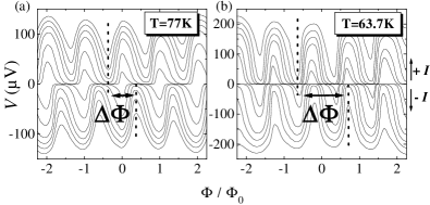
The clear-cut experimental determination of requires the measurement of -curves at various values of , which can be varied by temperature. An example of such a measurement on one device at K and 63.7K is shown in Fig.2.

Plotting the measured flux shift, normalized by vs. should give according to Eq.(5) a linear dependence with slope 1, with the reasonable assumption that does not depend on . Fig.3 shows the results of such measurements obtained for 6 different dc SQUIDs, where was obtained as a fitting parameter to give the expected slope of 1. For comparison, the results from simulated -curves for various values of are also shown, which are in excellent agreement with Eq.(5).
Except for one device, these SQUIDs have intentionally been fabricated with a geometric asymmetry (). From the known value of and the measured value of the asymmetry parameter can be calculated using Eq.(4). The results are listed in Table I. As a main result, we see that 3 SQUIDs show only a small asymmetry in with . However, for the three other devices the asymmetry in is significant with values of up to 0.4, which demonstrates that the difference in critical current density for the two junctions can be quite large.
| # | 1 | 2 | 3 | 4 | 5 | 6 |
|---|---|---|---|---|---|---|
| 0 | 0.33 | 0.33 | 0.33 | 0.5 | 0.5 | |
| 0.1 | 0.05 | 0.3 | 0.4 | 0.12 | 0.14 | |
| 0.1 | -0.29 | -0.04 | 0.08 | -0.4 | -0.39 |
IV transfer function: numerical simulations
As already evident from Fig.2 the asymmetry can induce distortions of the -curves, which leads to different values of and for the maximum positive and negative slope of the -curves, respectively. To understand the impact of the asymmetry on the transfer function we performed numerical simulations to solve the equations for the phase differences and of the two junctions [2, 3] over a wide range of values for and the noise parameter for both, the geometric and intrinsic asymmetry. In the latter case we assume the correlation between and as given in Eq.(3).
Figure 4 shows and vs. obtained for fixed for geometric and intrinsic asymmetry.


For we closely reproduced the results obtained in [1] for symmetric dc SQUIDs. In most cases we find for for the asymmetric SQUID a reduction of as compared to the symmetric SQUID , which increases with decreasing and increasing . However, in the case of geometric asymmetry, we find for intermediate values of an increase in for =, which is concomitant with a strong distortion of the -characteristics. If we assume , we find that for geometric asymmetry is always larger than for intrinsic asymmetry (for given ). This implies that the distortion in is dominated by the asymmetry in the junction resistances which becomes important for . At the reduction of and is similar for both types of asymmetry, indicating that for small the asymmetry in the critical currents gives the main contribution to .
Results similar to those shown in Fig.4 have been obtained over a wide range which corresponds to 4pH160pH for the SQUID inductance at =77K where pH. We note that for the symmetric dc SQUID it was shown in [1] that the normalized transfer function factorizes in where is given as . As a main result of our simulations for the asymmetric dc SQUID we find a similar factorization, with being now also dependent on , while shows no dependence on . For this is shown in Fig.5(a) for geometric and in Fig.5(b) for intrinsic asymmetry. The simulation data shown in Fig.5 can be approximated as
which is plotted in Fig.5 as dotted lines. These equations enable one to calculate immediately for any value of , and , however only within the range of parameters displayed in Fig.5. Similar behavior was found for , again with the factorization with . For we did not derive expressions as for given in Eqs(LABEL:eq-gf-plus). As discussed above for the resistance asymmetry plays an important role. Its impact on needs to be studied in more detail.
V transfer function: numerical simulation vs. experiment
To test the numerical simulation results we determined for various YBCO dc SQUIDs (#2-6 from Table I) with and at =77K. Figure 6 shows that the simulation (open symbols) predicts a reduction of both, and as compared to the symmetric case.
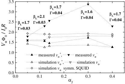
For the experimental data (solid symbols) lie between the values predicted for the symmetric and asymmetric case. For the measured and calculated values for are identical and lie almost a factor of two below the value predicted for the symmetric SQUID. This supports the idea that at least part of the discrepancy in between calculated and measured values can be attributed to asymmetry. However, most measured values for are clearly larger than predicted for either the symmetric or the asymmetric SQUID. The reason for this deviation is most likely due to the large uncertainty in the value for , which induces an increasing distortion with increasing [2, 6].
We finally note that a clear-cut comparison between simulation and experimental data for requires the experimental determination of at least , and preferably also of for a wide variety of HTS dc SQUIDs. Unfortunately, an extensive collection of such data does not exist yet. In order to obtain at least some information on the importance of asymmetry as a possible source for the discrepancy in between theory und experiment we show in Fig.7 the prediction for symmetric dc SQUIDs (dotted line) compared with experimental data taken from the literature [1].

In addition, the large open symbols show our simulation results obtained for various values of , assuming intrinsic asymmetry with . Obviously, the observed deviations between experiment and simulation for symmetric SQUIDs cannot be explained by asymmetry for large values of . For smaller values of , however, most of the experimental data lie within the range of values covered by simulations which take into account asymmetry in the SQUID, although a large reduction of due to asymmetry, say by a factor of five requires a very large .
VI Conclusions
We have analyzed the performance of asymmetric HTS dc SQUIDs both experimentally and by numerical simulation, with focus on transfer function. Our simulations show that strong critical current asymmetry which may arise from a large spread in critical currents in HTS Josephson junctions can significantly reduce for small . This observation is important, since optimum performance requires the realization of small . We wish to stress that the asymmetry, which is most likely present in almost all HTS dc SQUIDs, may be one source for the previously found discrepancy in between experiments and simulations, however it is not likely that this asymmetry is the major source of this discrepancy.
Acknowledgment
We gratefully acknowledge valuable support from Knut Barthel and Alex I. Braginski.
References
- [1] D. Koelle, R. Kleiner, F. Ludwig, E. Dantsker, J. Clarke, ”High-transition temperature superconducting quantum interference devices,” Rev. Mod. Phys., vol. 71, pp.631-686, April 1999.
- [2] R. Kleiner, D. Koelle, F. Ludwig, E. Dantsker, A. H. Miklich, J. Clarke, ”Current amplification with asymmetric direct current superconducting quantum interference devices,” J. Appl. Phys., vol. 79, pp.1129-1142, January 1996.
- [3] C. D. Tesche, J. Clarke, ”dc SQUID: Noise and Opitimization”, J. Low Temp. Phys., vol. 29, pp.301-331, 1977.
- [4] K. Barthel, D. Koelle, B. Chesca, A. I. Braginski, A. Marx, R. Gross, R. Kleiner, ”Transfer function and thermal noise of direct current superconducting quantum interference devices operated under large thermal fluctuations,” Appl. Phys. Lett., vol. 74, pp.2209-2212, April 1999.
- [5] R. Gross, L. Alff, A. Beck, O. M. Froehlich, D. Koelle, A. Marx, ”Physics and technology of high temperature superconducting Josephson junctions,” IEEE Trans. Appl. Supercond., vol. 7, pp.2929-2935, June 1997.
- [6] J. Müller, ”Asymmetrische Quanteninterferenzdetektoren aus Hochtemperatursupraleitern”, Diploma Thesis, Universität zu Köln, March 2000, unpublished.