Abstract
DC and AC electrical measurements were performed to investigate the electrical conductivity of samples with different concentrations of centers (Mg ions each with a trapped hole) in the temperature interval 250-800 K. The concentration of centers was monitored by the optical absorption peak at 2.56 eV. These centers were produced by oxidation at temperatures above 1050 K. The formation rate of centers depends on the previous thermal history of the sample in either reducing or oxidizing atmosphere.
At low electrical fields, DC measurements reveal blocking contacts. At high fields, the I-V characteristic is similar to that of a diode (corresponding to a blocking contact at one side of the sample and an ohmic contact at the other side) connected in series with the bulk resistance of the sample. Steady electroluminescence is emitted at the negative electrode when a current in excess of 10 passes through the sample, indicating that the majority of carriers are holes.
Low voltage AC measurements show that the equivalent circuit for the sample is the bulk resistance in series with the junction capacitance (representing the blocking contacts) connected in parallel with a capacitance, which represents the dielectric constant of the sample. The values determined for the bulk resistance in both DC and AC experiments are in good agreement. The electrical conductivity of crystals increases linearly with the concentration of centers, regardless of the amount of other impurities also present in the crystals, and is four times higher in the than in the direction. The conductivity is thermally activated with an activation energy of 0.68 eV, which is independent of: 1) the content, 2) the crystallographic orientation, and 3) the concentration of other impurities. These results favor the small-polaron-motion mechanism.
cond-mat/YYYY
December-2000
SEMICONDUCTING CHARACTERISTICS OF
MAGNESIUM-DOPED SINGLE CRYSTALS.
M. Tardío ⋆, R. Ramírez, R. González
Departamento de Física
Escuela Politécnica Superior
Universidad Carlos III de Madrid
Avda. de la Universidad 30,
28911 Leganés (Madrid), Spain
Y. Chen
Division of Materials Sciences,
Office of
Basic Energy Sciences, SC 13, Germantown
MD 20874-1290, USA
and
M.R. Kokta
BICRON Crystal Products, Washougal
Washington 96871, USA
Key words: Electrical conductivity, ,
center, :
e-mail:
mtardio@fis.uc3m.es
I. INTRODUCTION
and cubic MgO crystals are well-known for their electrical insulating properties. In ideally pure systems one would expect that replacing the host cation with an aliovalent impurity would result in either electron or hole conduction. This has not been realized, simply because of the presence of other impurities, which serve as charge-compensators for the intended dopant.
Nevertheless, semiconducting properties have been observed in MgO doped with lithium, and the physics involved has been reported. [2, 3, 4, 5] There are similarities between and lithium-doped MgO crystals: 1) After oxidation at high temperatures, hole-trapped centers are formed in both oxides. In the latter, centers (substitutional ions, each attended by a hole) are produced at T 1100 K, which absorb light at 1.8 eV (690 nm).[6, 7, 8] 2) In MgO:Li crystals, hole-trapped centers are also responsible for the electrical conductivity enhancement observed. [5] MgO crystals containing centers have been shown to be p-type semiconducting at temperatures not much higher than RT, with an acceptor level of 0.7 eV. [5] By analogy, crystals are expected to serve as a p-type semiconductor. Both systems have potential as high-temperature semiconductors. However, whereas the former is brittle and will have limited applications, the latter is expected to have superior mechanical integrity.
As-grown single crystals of magnesium-doped exhibit a gray-purple coloration, which becomes much stronger after quenching these crystals from above 1173 K in an oxidizing atmosphere. [9, 10, 11] This coloration is due to a broad asymmetric optical absorption band, centered at 2.5 eV (496 nm), and has been attributed to the paramagnetic hole-trapped center, which is a substitutional ion with a trapped hole localized on one of the six NN oxygen ions. [9, 10] These centers are stable up to 850 K. In a reducing atmosphere centers vanish at temperatures above 850 K. Thermal treatments between 850 K and 1250 K in air turn the samples colorless.
Nominally pure has a reported [12, 13] conductivity varying from at room temperature to at 1773 K. The effect of magnesium doping on its electrical conductivity has been previously [10, 14] studied at elevated temperatures (1673-1873 K ), and the value reported at 1773 K is ; this increase in conductivity was attributed to holes released from centers moving as large polarons with an activation energy of 0.68 eV. [10] However, recent theoretical calculations [15] in suggest that holes exist as small polarons and their optical absorption energy is 2.9 eV. The energies required for polaron hopping between neighboring positions is 0.9 eV. [15]
In the present work, the electrical properties of containing centers were studied at moderate temperatures (from 250 to 773 K), i.e. at temperatures where centers are stable. Both AC and DC electrical measurements were performed. At RT, the resulting values for the conductivity are ten orders of magnitude higher than those reported for undoped samples. The conductivity dependence on content was investigated. The effect of the temperature on the conductivity along different crystallographic directions was analyzed, and provided information about the conductivity mechanisms. Our results favor the small polaron model. [15]
II. EXPERIMENTAL PROCEDURE
The single crystals were grown separately by the Czochralski method (the ambient growth atmosphere was an inert gas with 1000 ppm by volume of oxygen), labeled as and . The latter had a higher magnesium concentration, but the concentration of other impurities was also higher. Measurements were primarily made in the crystal. crystal was used for comparison. Atomic Emission Spectrometry analyses indicated that for crystal the magnesium concentration was 25 ppm; other known impurities were Ti ( 10 ppm), V ( 3ppm), Cr ( 3 ppm), Mn ( 5 ppm), Fe (10 ppm), and Ni ( 5 ppm). For crystal , the magnesium content was 57 ppm and other impurity concentrations were: Ti (35 ppm), V ( 3ppm), Cr (10 ppm), Mn (5 ppm), Fe (60 ppm), and Ni (6 ppm). Samples of about 1 mm thick were cut from the boule with either the c-axis parallel or perpendicular to the broad face, and polished to optical transparency. Optical absorption measurements were made with a Perkin-Elmer Lambda 19 Spectrophotometer.
Heat treatments either in static air or in flowing oxygen were made with the samples placed in a platinum basket inside an alumina tube inserted in a horizontal furnace. Reduction treatments were performed in a high-purity graphite capsule surrounded by flowing nitrogen gas inside the furnace. Subsequently, the samples were pulled out from the hot zone and fast-cooled in the room-temperature portion of the tube.
For DC measurements, voltage was applied to the crystals with a DC Sorensen DCS 150-7 voltage source. I-V characteristics were measured with an electrometer (Keithley 6512) and a voltmeter (HP 34401A). A standard three electrical-terminal guard technique was used. [16] For AC measurements, a function generator was used, where available frequencies range from to Hz.
Electrodes were made by sputtering metals with different work functions (Al, Mg and Pt) onto the sample surfaces, usually the largest faces. The electrical response was independent of contact electrode materials, so mostly Al electrodes were used. The samples with the electrodes were placed in a sample holder, which can be used for measurements below room temperature (using a temperature controlled thermal bath) and for temperatures above room temperature using a conventional horizontal furnace. Electrical measurements were performed in static air. The temperature of the sample was monitored with a Chromel-Alumel thermocouple in direct contact with the sample.
III. EXPERIMENTAL RESULTS
A. Characterization by optical absorption
The polarized optical absorption spectra of a sample from before and after different thermal treatments are shown in Fig.1. In the as-grown state (trace a), a broad asymmetric absorption band covering the visible region is observed. The high energy side of this band extends into the UV part of the spectrum. The low energy side, extending into the infrared, has an approximately Gaussian shape peaking at 2.56 eV. This band is the analog of the center in MgO:Li and has previously been associated with centers. [9, 10] The presence of these hole-trapped defects in as-grown samples is indicative of the presence of oxygen during the crystal growth process. Indeed, annealing of the latter crystals in a reducing atmosphere (or in air) at 1200 K for 45 min, completely annihilates this band (trace b). For comparison, the absorption spectra of an as-grown undoped crystal are also shown in the dotted curves. The higher absorption in the UV region is probably due to charge-transfer bands of transition metal ions. [17]
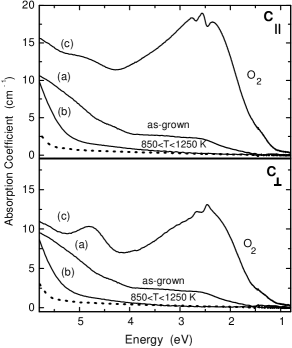
After oxidation of the as-grown crystal at 1923 K for 30 min, the absorption of the 2.56 eV dramatically increased and another band at about 4.75 eV (260 nm) emerged, which can be better resolved in the spectrum taken with light polarized perpendicular to the c-axis. The structure on top of the 2.56 eV band is better resolved as the oxidation temperature is increased. Its origin is unknown. In addition, the intensity of the 2.56 eV band is higher for the spectrum with light propagating parallel to the c-axis. The ratio between the two absorption coefficients is 1.5.
The concentration of centers can be estimated from the experimentally deduced [10] relationship
| (1) |
where N() denotes the concentration of centers and ) is the absorption coefficient of the 2.56 eV band. The resulting concentration for the sample oxidized at 1923 K is 1.20 or 12 ppm, indicating that approximately half of the magnesium is dissolved in the crystal in the configuration.
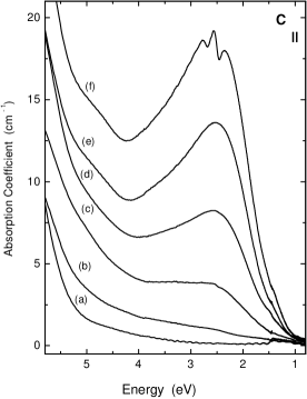
Another sample from , initially annealed in air to remove the 2.56 eV band, was oxidized for 30 min periods at increasing temperatures in flowing oxygen up to 1923 K. Fig.2 shows the growth of the center band for several selected temperatures. After the anneal at about 1100 K, the 2.56 eV band began to emerge. The absorption increases monotonically with temperature up to about 1923 K and then saturates. The UV absorption at 4.75 eV, which is more pronounced in the c direction, also increases with the oxidation temperature. We associate this band with a Mg-related defect because undoped crystals or those doped with other impurities do not show this band after oxidation at elevated temperatures.
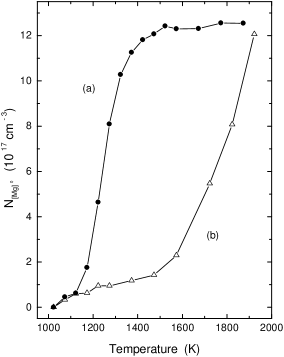
Prior thermal history either in reducing or oxidizing atmosphere has a strong influence on the formation rate of centers induced by oxidation. Two similar samples from the crystal were subjected to thermal treatments in different atmospheres. One as-grown sample was reduced in graphite at 1223 K for 20 min until the centers vanished. The second as-grown sample was first oxidized at 1723 K for 2 h before reducing at 1223 K for 20 min. These two samples were then isochronally heated in flowing oxygen for 30 min (see Fig.3). The threshold temperatures for the formation of centers are the same in both cases 1050 K. However, the production curve is much more rapid for the pre-oxidized sample (curve a). The concentration saturates at 1500 K with 1.3 . Without pre-oxidization (curve b) the same concentration was attained only after 1923 K, which is the maximum capability of our furnace.
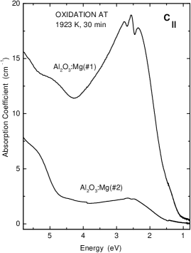
A sample from the crystal, which has twice the concentration of magnesium as from , generates fewer centers upon oxidation (Fig.4). Whereas in sample , 50% of the magnesium forms centers, in sample it was only 3%. This finding clearly shows that the resulting concentration depends on the content of magnesium as well as other impurities. Presumably, other impurities, mainly Ti and Cr, prevent the trapping of holes by oxygen ions located as nearest neighbors of the ions. Higher oxidation states such as and compensate ions substituting for ions. Indeed, the sample has a relatively higher absorption in the UV region.
B. Electrical Measurements
To investigate the electrical conductivity of crystals, DC and AC electrical measurements were performed in samples with different concentrations of centers in the temperature range 250-800 K. Unless otherwise indicated, electrical measurements were made in samples where oxidation induces a higher concentration of centers.
1. DC electrical properties
DC electrical measurements at low electric fields reveal blocking contacts. However, at high fields, the reverse bias characteristic is that of a ”soft” leaky barrier. A typical forward-bias current-voltage (I-V) characteristic is shown in Fig.5 for a sample with a concentration of 1.20 . This characteristic is similar to that of a diode with a series resistance, , which corresponds to a blocking contact at one side of the sample and an ohmic contact at the other side; the series resistance is the bulk resistance of the sample. The experimental points are plotted as open circles, and the solid line represents the best fit of the data to the equation:
| (2) |
which corresponds to a forward biased diode in series with a resistance. Here n is the ideality factor of the junction, q is the carrier charge, and is the saturation current.
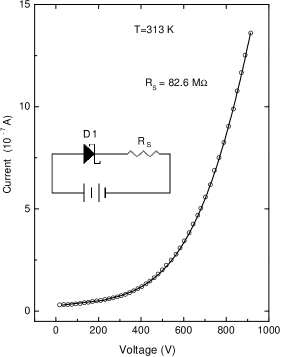
Blocking contacts are expected for hole conduction in wide band gap insulators, but since the electrodes are symmetric (the metal is the same in both), there should be no ohmic contact. On reversing the applied voltage, practically the same I-V characteristic is obtained. This result appears to be in contradiction with having an ohmic contact on one side and a blocking contact on the other: a given polarity would imply a forward bias in the barrier (a direct current flows through the sample), whereas the opposite polarity should induce a reverse bias in the barrier, and small and voltage-independent values for the current should be observed.
Symmetry requires that blocking contacts are formed on both sides of the sample. In this way, regardless of the polarity of the applied voltage, one of the contacts is forwardly biased, while the other is reversely biased; on increasing the applied voltage, breakdown can occur in the reversely biased contact. For sufficiently high voltages, the overall behavior of the sample is that of an ohmic contact with a series resistance (the bulk resistance) and a forward biased blocking contact. Three parameters can be obtained from a fit of the experimental I-V characteristics: the bulk resistance, the ideality factor of the junction, and the saturation current. The values of the last two parameters are affected mainly by the shape of the low voltage part of the I-V curve. On the other hand, the initial part of the characteristic is probably influenced by the breakdown peculiarities in the reversed direction and the values derived for n and are not fully reliable. Regarding the value obtained for the series resistance, it provides an order of magnitude for the sample, as the AC results following this section will show. The association of the ohmic part of the I-V curve with the sample resistance is based on the fact that the same value for the conductivity was determined using samples with different thickness, d, and cross-section, S.
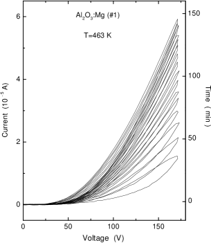
As the temperature is raised, the bulk resistance diminishes; it is not feasible to apply the high voltages needed to break the blocking contact because of Joule dissipation in the sample. At medium voltages, the rupture mechanisms of the blocking contact reveal a complex behavior; since neither the electrodes nor the sample surface is homogeneous on a small scale, some regions of the contact can be broken at medium voltage values, while others depend on temperature and time the voltage is applied. This behavior is illustrated in Fig.6 for a sample subjected to subsequent voltage ramps (the right axis represents the time at the maximum applied voltage). The slope of the I-V curve increases with time, implying that the resistance diminishes; also there is some hysteresis due to Maxwell-Wagner polarization phenomena at shorter times. [11, 18, 19] These two observations indicate that the area of the broken contact increases with time, thereby diminishing the total resistance and the polarization effects. If the whole contact is broken, the resistance should be equal to the sample resistance.
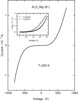
Additional information on the non-homogeneity of the contacts is shown in Fig.7. The I-V curve is non-symmetric with respect to voltage polarity, probably because the size of the contact regions that experience breakdown is different on each electrode. To obtain symmetric curves special care must be taken to assure that sample preparation and electrode deposition are identical in both electrodes. Another important outcome of the DC measurements is the emission of electroluminescence (EL): when a current in excess of 10 passes through the sample, steady light has been observed with the naked eye to emerge from a narrow region at the negative electrode [20]. No emission was observed from the positive electrode. The light intensity is proportional to current intensity above the threshold. Several EL bands have been resolved and related to photoluminescence emissions of different extrinsic defects, such as ions. These results have been interpreted based on the assumption that the majority carriers flowing through the sample recombine with the minority carriers injected from the negative electrode [20]. EL emission occurring at the negative electrode indicates that the majority carriers are holes. The steady emission and its proportionality with current and voltage reveals that ohmic conduction is taking place.
As mentioned in the experimental section, we used three metals as electrodes, Mg, Al and Pt, with widely different work functions: 3.6, 4.2 and 5.6 eV, respectively. The results described in this section are independent of the types of metal used as electrodes. This indicates that the barrier formed at the electrodes is dominated by surface effects.
The relevant conclusion of DC measurements in crystals containing centers is that upon application of a moderate electric field there is a flow of direct current through the sample, which is ohmic in the high voltage regime, and is governed by the bulk resistance. Surface and electrode effects make the interpretation of these measurements difficult and sometimes not quantitatively reproducible. Some of these difficulties can be overcome by AC electrical measurements.
2. AC electrical properties
The equivalent circuit for low voltage AC measurements consists of in series with (junction capacitance, which accounts for the blocking nature of the contacts) and , which represents the dielectric constant of the sample (see Fig.8 insert).
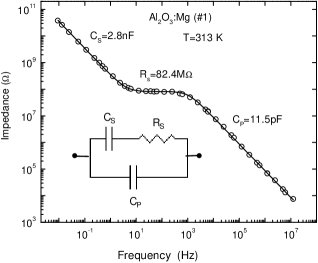
Fig.8 is a log-log plot of the AC impedance versus frequency for a sample with an electrode area of 0.85 and a thickness of 0.10 cm, at a fixed temperature of 313 K. The experimental values are plotted as open circles, and the solid line is the best fit to the equivalent circuit. A value of 11.5 pF for is consistent with the dielectric constant of . The results presented in Figs.4 and 7 were measured in the same sample and at the same temperature; the values determined for in both DC and AC experiments are in good agreement.
The values obtained for depend on the quality of the sample
surface. Fig.9 shows two log-log plots of impedance versus
frequency in a sample with a concentration of centers of 1.34 (S = 0.75 and
d = 0.12 cm). The two curves correspond to the sample with
two degrees of surface polishing; the values of = 2.7 and
12.7 nF were obtained for the sample with an intermediate and
final polishing, respectively. After a DC current flowed through
the sample for 24 h at a constant temperature of 348 K, the
value dropped to 7.2 nF. Subsequently, the sample was heated at
600 K for several hours with a small AC applied voltage and
dropped further to 2.7 nF. Since is more than
one thousand times smaller (8.4 pF), a value of 12.7 nF for
suggests a depletion layer thickness slightly smaller than one
micron, which seems to be reasonable. The diminishing with
the flow of DC current is attributed to the presence of traps in
the depletion layer. The hysteris behavior of ( does
not recover its original 12.7 nF value) can be attributed to deep
traps at the depletion layer. Unfortunately, characterization of
these traps, for instance by deep level transient spectroscopy
(DLTS), is prohibitive since the high impedance of the sample
requires the use of very low frequencies for these measurements.
In addition, the ionization temperature of these traps would
require that the sample be heated at temperatures at which the
centers are unstable. Lastly, the values are observed
to be independent of the metal used as electrodes.
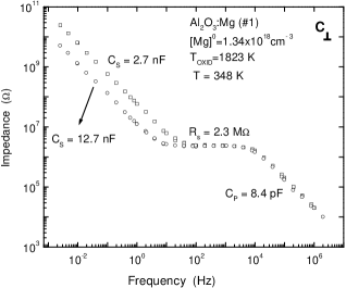
Fig.9 also shows the frequency regions in which the resistance and parallel capacitance, and dominate ( 102 Hz). These values are independent of the quality of the sample surface. The values in the AC measurements are reproducible and yield consistent values for the sample conductivities.
We have also tried to perform a (V) characterization, the dependence of the junction capacitance on the voltage bias. Within the voltage range (0-100 V) investigated, is independent of the voltage bias. However, these measurements are difficult because low frequency values are necessary. On the other hand, and of greater importance, the barrier is ”leaky”, so upon application of a bias voltage some regions of the barrier junction are broken. Thus, the results of low-voltage AC measurements reinforce the interpretation from DC measurements that blocking contacts exist in a resistive sample.
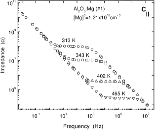
The temperature dependence of the three parameters , and can be deduced from Fig.10. AC measurements at four different temperatures were made in a sample with a concentration of 1.21 centers. The basic results are: and are practically independent of temperature in the temperature range 273-423 K, whereas the sample resistance diminishes as temperature increases.
Next, we will address the electrical conductivity and its dependence on temperature and concentration. We have already mentioned that experiments using different sample geometries confirm that the resistance is directly related to the sample conductivity, thus the dependence of the conductivity on temperature and content can be inferred from measurements. Figs.11 and 12 show respectively the Arrhenius plots of the sample conductivity perpendicular and parallel to the crystallographic c-axis for samples containing different concentrations of centers. The data plotted in the top part of these figures were obtained from different samples cut from the crystal, while the bottom part refers to only one sample (also from subjected to oxidizing treatments at increasing temperatures. After each anneal the AC measurements were performed at different temperatures. The solid circles in Fig.12 are data for an sample oxidized at 1923 K for 30 min. The slope of these plots is the same, indicating that the conductivity is thermally activated with an activation energy of 0.68 eV. The parallelism of the straight lines indicates that this value is independent of: 1) the content, 2) the crystallographic orientation, and 3) the amount of other impurities. However, the conductivity depends on the crystallographic direction, and is four times larger in the direction parallel than in the directions perpendicular to the c-axis.
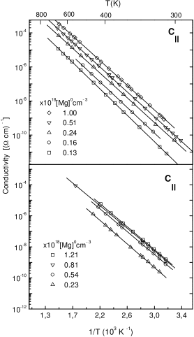
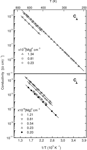
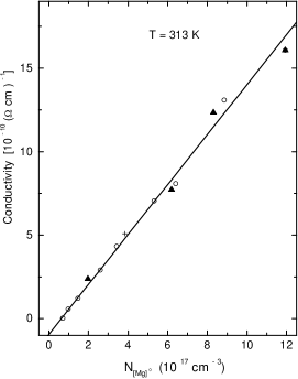
Fig.13 shows the dependence of the conductivity on center concentration at T = 313 K. The conductivity was measured perpendicular to the c axis. The four solid triangles correspond to one sample from oxidized at four isochronal temperatures for 30 min each. Open circles represent the data obtained from eight samples also cut from the crystal. Each sample was oxidized at a different temperature to produce a different concentration of centers. Lastly, the cross corresponds to a sample cut from the crystal and subsequently oxidized at 1923 K for 30 min. These results clearly show that there is a linear relationship between conductivity and content, regardless of the thermal history and content of other impurities.
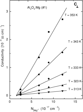
To explore this linearity further, the electrical conductivity dependence on the content was investigated in the same sample at five temperatures: 313, 323, 333 343 and 353 K. The conductivity perpendicular to the c axis was measured. The concentration was varied by subjecting the sample to increasing temperatures in flowing oxygen. After each oxidation, the amount of centers in the sample was measured, and its conductivity was determined at the five temperatures indicated. The results are plotted in Fig. 14. In all the cases, a linear relationship between conductivity and concentration was also observed.
IV. DISCUSSION
Our experimental results show that the electrical conductivity of crystals is governed by centers in direct proportion with the concentration. The presence of other impurities serves to reduce the resulting concentration. The conductivity is thermally activated with an activation energy of 0.68 eV. The conductivity anisotropy factor is four with greater than .
The thermally-activated behavior of conductivity can be explained by any of three different mechanisms: impurity conduction, [21, 22] standard semiconducting behavior [23] or small polaron motion. [24, 25] We shall discuss these three mechanisms in relation to the electrical conductivity results.
Impurity conduction may be ruled out because this mechanism implies a strong dependence of the activation energy on impurity content (in this case centers) and on the concentration of compensating impurities. [21, 22] Our results give the same activation energy over a broad range of concentration. In addition, samples with large Mg concentration compensated by large concentrations of compensating impurities yield the same activation energy.
The standard semiconducting mechanism yields [23] a thermally activated behavior for the concentration of carriers, p, in two different regimes:
a) At low temperatures, p and p ; here and are the concentrations of acceptor and compensating impurities, respectively, and the effective density of states in the valence band. The concentration of carriers is given by:
| (3) |
where is the acceptor ionization energy.
b) When the temperature is high enough for p and p , but low enough for not having all the acceptors ionized (kT ), then:
| (4) |
The conductivity in both cases is , where is the mobility, which usually varies as a power of the temperature (depending on the carrier scattering process) and is independent of the acceptor concentration for concentrations that are not too large. In the second temperature regime, the conductivity is proportional to the square root of the acceptor concentration at a given temperature, which is not our case. So we are left with the behavior given by Eq. 3, which provides a linear relation between conductivity and acceptor concentration. This result agrees with our findings. However, according to Eq. 3, the slope of the conductivity plotted against acceptor concentration depends on the concentration of compensating impurities. We know that these concentrations are very different in and crystals. Fig. 14 shows that the slope of the conductivity versus is independent of the concentration of compensating impurities.
Within this framework it is also difficult to establish a link between the activation energy of the conductivity and the optical absorption energy associated with centers (0.68 eV versus 2.56 eV). It should be noted that for ionic crystals, polar optical scattering of carriers may be the dominant process in the mobility, leading to a temperature dependence of the mobility given by:
| (5) |
where is the angular frequency of an optical phonon and , is of the order of 0.01 eV (typical for a high energy phonon).
This mobility behavior together with an increase of the effective mass is known as large polaron. [26, 27] Taking into account that the measured activation energy for the conductivity is 0.68 eV and using Eq. 5, the activation energy for carrier ionization is estimated to be 0.67 eV, which is still far from 2.56 eV. Therefore we conclude that the standard semiconducting mechanism does not satisfactorily explain the experimental results.
The third mechanism is small polaron motion. [24, 25] In some materials where the interaction between carriers and lattice vibrations is sufficiently strong, an excess carrier will find it energetically favorable to remain localized in one of an infinite number of equivalent sites of the crystal. The carrier-lattice interaction induces a lattice distortion in the immediate vicinity of the carrier. The potential well produced by this distortion in turn acts as a trapping center for the carrier; this self-trapped unit is called small polaron. [24, 25]
At temperatures above approximately one half of the Debye temperature, small polaron motion occurs by thermally activated hopping. Also, polarons have an associated broad optical absorption band at photon energies four times larger than the hopping activation energy. [24, 25] In our case, this represents 2.72 eV, which fits quite well with our observations of 2.56 eV. The small discrepancy can be due to the electrical field caused by the substitutional ions (which are negatively charged with respect to the lattice) on the polaron.
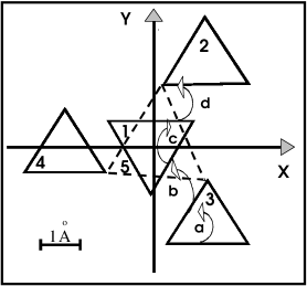
In addition to this phenomenological approach to small polarons, atomistic simulations of self-trapping of holes in have recently been carried out. [15] These calculations lead to the conclusion that self-trapped holes are energetically more favorable than free holes, and that the optical absorption energy of the self-trapped hole is 2.9 eV. The energies required for the self-trapped polaron to jump between equivalent positions through the lattice were also determined. In Fig.15, two types of oxygen triangles are shown: the so-called small triangles (1, 2, 3 and 4) and a big triangle (5). Triangle 1 lies 2.17 Å above triangles 2,3,4 and 5; the self-trapped hole is shared by two of the oxygen atoms in a small triangle; hops inside the small triangle (involving reorientation) require the same activation energy ( 0.9 eV) as hops from a small triangle (such as 3 in Fig. 15) to another small triangle lying below or above it such as 1. Any other type of hop requires a much higher activation energy. Within this picture, a displacement along the c-axis requires one hop (and is 2.17 Å long), while a displacement to an equivalent position along a direction perpendicular to the c-axis requires four steps: one hop to a triangle lying in another plane, a reorientation in this triangle, another hop back to the same plane and a final reorientation (here, the displacement along the direction of motion is 4.76 Å). Although the hop activation energy of 0.9 eV is not inconsistent with our value (0.68 eV), [28] the anisotropy in the conductivity yields a value of two instead of four (which is our result). This discrepancy can only be explained in terms of the frequencies of the phonons involved in the reorientations and in the hops between triangles lying in different planes, since the attempt frequency of each hop is proportional to the phonon frequency. In the above description the activation energies for the conductivity along the directions parallel and perpendicular to the c-axis are the same as were found in our experiments.
Hall effect measurements could clarify the type of carrier involved in the electrical conduction. However, we were unable to perform these measurements because of the high impedance of the samples, and probably because of their blocking contacts. It was not possible to measure photocurrents, which could be helpful to determine the drift mobility of carriers and provide a definite answer as to whether holes are self-trapped or not.
V. SUMMARY AND CONCLUSIONS
Optical absorption measurements at 2.56 eV were used to monitor the concentration of centers in two crystals of intentionally doped with different concentrations of magnesium. While the Mg concentration was higher in one crystal, the unintended levels of impurities were also higher. The net effect was a diminished concentration because of charge compensation. centers are formed at temperatures above 1050 K in an oxidizing atmosphere. The increase in concentration with temperature depends dramatically on the thermal history of the sample. For samples pre-oxidized at high temperatures, centers form very rapidly and their concentration saturates at 1500 K. For a non pre-oxidized sample, the saturation value is achieved after an anneal at 1923 K.
DC and AC electrical measurements were performed to investigate the electrical conductivity of samples with different concentrations of centers in the temperature interval 250-800 K.
At low electrical fields, DC measurements reveal blocking contacts. At high fields, the I-V characteristic is similar to that of a diode (corresponding to a blocking contact at one side of the sample and an ohmic contact at the other side) connected in series with the bulk resistance of the sample. The non-homogeneity of the contacts is responsible for the asymmetry of the I-V curve with respect to voltage polarity. In addition, when a current in excess of 10 passes through the sample, steady EL emission has been observed to emerge from the negative electrode, [20] indicating that the majority carriers are holes. The intensity of the light is proportional to current intensity and voltage, showing that ohmic conduction occurs. Low voltage AC measure ments show that the equivalent circuit for the sample is a series combination of the bulk resistance, , and junction capacitance, , (representing the blocking contacts) connected in parallel with a capacitance, , which represents the dielectric constant of the sample. The values determined for the bulk resistance in both DC and AC experiments are in good agreement. In the temperature range 273-473 K, diminishes as temperature increases, whereas and remain practically constant. The electrical conductivity of crystals increases linearly with the concentration of centers. Other impurities serve as charge compensators to prevent the formation of centers. The conductivity is anisotropic, with the parallel direction four times higher than in the perpendicular directions to the c-axis. The thermal activation energy is 0.68 eV, which is independent of: 1) the content, 2) the crystallographic orientation, and 3) the concentration of other impurities.
Neither impurity concentration [21, 22] nor standard semiconducting [23] mechanisms can adequately explain the observed thermally-activated behavior of the conductivity. A small-polaron-motion mechanism [24, 25] provides a more likely explanation. In this mechanism, the interaction between an excess carrier and the lattice induces a lattice distortion in the immediate vicinity of the carrier. [24, 25] The potential well produced by this distortion traps the carrier, thereby creating a small polaron. [24, 25] Our experimental findings are consistent with the predictions of the small-polaron-motion mechanism, with the exception that the experimental value of four is larger than the theoretical anisotropy of two. This discrepancy is associated with the frequencies of the phonons involved in the self-trapped polaron motion.
Acknowledgments
Research at the University Carlos III was supported by the CICYT of Spain. The research of Y.C. is an outgrowth of past investigations performed at the Solid State Division of the Oak Ridge National Laboratory.
References
- [1]
- [2] D.J. Eisenberg, L.S. Cain, K.H. Lee and J.H. Crawford, Jr., Appl. Phys. 33, 479 (1978).
- [3] Y. Chen, M.M. Abraham, J.L. Boldú, and V.M.Orera, J. Phys.(Paris) Colloq. 41, 398 (1980).
- [4] Y. Chen, R. H. Kernohan, J.L. Boldú, M.M. Abraham, D.J. Eisenberg and J.H. Crawford, Jr., Solid State Commun 33, 441 (1980).
- [5] R. Ramírez, R. González, R. Pareja and Y. Chen, Phys. Rev. B 55, 2413 (1997).
- [6] M.M Abraham, Y. Chen, L.A. Boatner and R.W. Reynolds, Phys. Rev. Lett. 37, 849 (1976).
- [7] Y. Chen, H.T. Tohver, J. Narayan and M.M. Abraham, Phys. Rev. B 16, 5535 (1977).
- [8] J. Narayan, M.M. Abraham, Y.Chen and H.T. Tohver, Phil. Mag. 37, 909 (1978).
- [9] R. T. Cox, Jr., Solid State Commun 9, 1989 (1971).
- [10] H.A. Wang, C.H. Lee, F. A. Kröger and R.T. Cox, Phys. Rev. B 27, 3821 (1983).
- [11] R. Vila and M. Jiménez de Castro, Phys. Rev. B 49, 1696 (1994).
- [12] F.G. Will, H.G. deLorenzi and K.H. Janora, J. Am. Ceram. Soc. 75, 295 (1992).
- [13] B. Evans, J. Nucl. Matter. 219, 202 (1995).
- [14] S.K. Mohapatra and A. Kröger, J. Am. Ceram. Soc. 60, 141 (1977).
- [15] P.W.M. Jacobs and E.A. Kotomin, Phys. Rev. Lett. 69, 1411 (1992).
- [16] R.M. Blumenthal and M.A. Seitz, in Electrical Conductivity in Ceramics and Glass (Marcel Dekker, New York, 1974), part A, edited by N.M. Tallan, p 106.
- [17] H.H. Tippins, Phys. Rev. B 1, 126 (1970).
- [18] L.K.H. Van Beek, Physical 26, 66 (1960).
- [19] R. Vila and M. Jiménez de Castro, J. Phys. D 25, 1357 (1992).
- [20] R. Ramírez, M.M. Tardío, R. González, M.R. Kokta, and Y. Chen, Radiat. Eff. Deff. S.(In Press) .
- [21] A. Miller and E. Abrahams, Phys. Rev. 120, 745 (1960).
- [22] M. Pollak and T.H. Geballe, Phys. Rev. 122, 1742 (1961).
- [23] K. Seeger, Semiconductor Physics (Springer, Berlin, 1989), pp 34-51.
- [24] I. Freidman and T. Holstein, Ann. Phys. (N.Y.) 21, (1963).
- [25] D. Emin and T. Holstein, Ann. Phys. (N.Y.) 53, 439 (1969).
- [26] H. Frölich, Adv. Phys. 54, 325 (1954).
- [27] A.J. Bosman and H.J. Van Daal, Adv. Phys. 19, 1 (1970).
- [28] A.L. Shluger and A.M.Stoneham, J. Phys.: Condenser Matter 5, 3049 (1993).