X-Ray Scattering Evidence for Macroscopic Strong Pinning Centers in the Sliding CDW state of NbSe3.
Abstract
Using high-resolution X-ray scattering techniques, we measure the variation, , of the position in reciprocal space of the CDW satellite, in the sliding state, along the length of NbSe3 whiskers. We show that structural defects and intentionally X-ray radiation-damaged regions increase locally the CDW pinning force, and induce CDW phase distortions which are consistent with those observed near contacts. Using the semi-microscopic model in Ref. [1] describing the normal condensed carrier conversion, with spatially varying parameters, we account for the experimental spatial dependence of the CDW phase gradient near both types of defects.
PACS numbers: 71.45.Lr, 72.15.Nj, 61.10i
In strongly anisotropic charge density wave (CDW) systems a phase transition of mixed structural and electronic character occurs at the Peierls temperature. The CDW ground state is characterized by a periodic modulation of the crystal lattice, accompanied by a periodic modulation of the electron density of same wavevector , where is the Fermi wave number [2, 3, 4].
In certain CDW materials, such as NbSe3, in which the wavelength of the CDW is incommensurate with the underlying lattice, sliding of the CDW as a collective motion is made possible by the application of an electrical current exceeding a threshold value . This collective charge transport is associated with remarkable electrical properties such as non-ohmic conductivity and narrow band noise (NBN) [5].
Phase slippage is the process by which conversion between free electron and CDW condensate occurs near the electrical contacts to a CDW conductor [6]. It proceeds via nucleation and growth of phase dislocations loops (DL) across the sample cross section [7]. Associated with the DL nucleation and growth process, the sliding-CDW phase is slightly distorted. The phase gradient is observable by means of X-ray diffraction as a longitudinal shift, , of the CDW satellite peak position in reciprocal space, [8, 9]. The CDW phase gradient has also been monitored by means of laser probe [10], electromodulated transmission [11], and conductivity measurements on multicontacted samples [12]. Even though all experimental data show qualitative agreement (the phase gradient exhibits maxima in the near contact regions and vanishes in the central part of the sample) there remains some controversies about the nature of the CDW-defect interaction [13, 14, 15]. While the above experiments reported phase distortions due to conversion near the electrodes, phase slippage is potentially needed near all defects of the strong pinning type.
In this paper, we show that a localised defect may act as a pseudo-electrode. Using high resolution X-ray diffraction, we monitored the shift, , of the NbSe3 sliding-CDW satellite as a function of beam position, , along two samples which exhibit, respectively, one and two localised structural defects between current electrodes. In addition to the near contact region, where the sliding-CDW phase is substantially distorted, we observe a similar phase distortion in the vicinity of the defects. A further experiment was performed by exposing part of sample ’2’ to the X-ray beam, over a long period of time, in order to damage it locally. In each case, the observed phase gradients are compared to numerical simulations based on the semi-microscopic model by Brazovskii et al. [1], describing the normal condensed carrier conversion. We give an estimate of the fraction of the CDW current which is converted, at the defect position.
NbSe3 has a chain-like structure, with chains parallel to the monoclinic -direction. It undergoes two independent Peierls transitions at 145 K and 59 K with modulation wave vectors ; =0.241 b∗ and ; =0.259 b∗, respectively. All measurements were carried out on the CDW satellite on the diffractometer TROIKA I (ID 10A) at ESRF (Grenoble/France) using an incident wavelength of 1.127 Ȧ ( keV). The sample orientation was such that the (a∗+c∗, b∗)-plane coincided with the horizontal scattering plane. In order to obtain a high spatial resolution, the beam width (from 10 to 30 m) was controlled by a slit, placed before the sample. The samples, of typical cross-sections 102 m2, were mounted on sapphire substrates of 100 m thickness to provide homogeneous sample cooling together with suitable beam transmission (50 %). Several types of electrical contacts were used. Two 2 m-thick gold electrodes, of 1 mm width, have been evaporated on Sample ’1’, leaving an uncovered section of 4.25 mm between electrodes. On sample ’2’, one 1 mm-wide electrode and one 15 m-wide electrode have been evaporated, leaving an uncovered section of 3 mm between electrodes.
The samples are selected for their high crystallographic quality. We scanned the (020) Bragg peak along the b* direction (() scans) and along the a*+c* direction (rocking scans), for several beam positions ( to m intervals). We tested a large number of samples from different origins [16], and we found that localised ( m-wide) growth defects appear very frequently in this material [17].
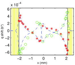
Fig. 1 shows the shift, , for positive and negative current polarities; I= mA (/=2.13), as a function of beam position, , along sample ’1’. This sample exhibits, between electrodes, one localised defect at the position . The sliding-CDW satellite shift changes sign abruptly at this position, with maxima on either sides of the defect position, as well as at the electrical contacts. In contrast, for defect-free samples, the phase gradient is large near the electrodes, where the conversion between normal carriers and CDW condensate occurs, and vanishes in the central section [1, 8].
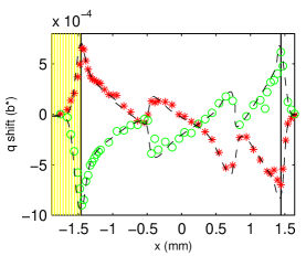
Fig. 2 shows the shift, , for positive and negative current polarities, I=3.5 mA (/=3), along sample ’2’, which exhibits, two localised defects at and . Again the shift changes value abruptly at these positions. Note incidentally that the CDW distortions extend over an appreciable distance ( m) beyond the contact boundary, regardless of the electrode width (15 m or mm). This behaviour has been confirmed on defect-free samples [18].
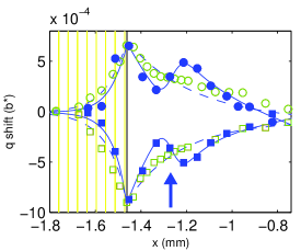
A further experiment was performed, by exposing sample ’2’ to a 30 m-wide X-ray beam, over a long period of time (4 hours), in order to locally create a damaged region. After the irradiation, the CDW satellite position changes value abruptly at the irradiated position (; the arrow position in Fig. 3). The open symbols in Fig. 3 show the shifts, , for positive and negative current polarities, as a function of beam position, , before the irradiation. The shift, , follows a typical monotonic decay in the near-contact region. The same measurements repeated after irradiation show a drastic change of the spatial dependence of the shift over a distance of approximately 200 m on either side of the irradiated position. The damage is also observed as a local broadening of the (020) Bragg reflection; this broadening is detected over a sample length of m around , which is consistent with the width of the irradiating beam. No significant longitudinal splitting of the CDW satellite was observed, near the defect, indicating that the cross section is homogeneously affected by the irradiation.
The semi-microscopic model by Brazovskii et al. [1], describing the normal condensed carrier conversion by nucleation and growth of dislocation loops in a highly rigid CDW electronic crystal gives a coherent fit of the spatial dependence of the CDW phase gradient, for homogeneous samples [1, 8, 19]. This model is based on the assumption of a local equilibrium between the electrochemical potentials of the phase dislocations, , and of the free carriers, :
| (1) |
where , and are, respectively, the normal carrier, CDW and total current densities. is the current density at threshold, and , the normal carrier conductivity. For high current values (), the friction force, , can be approximated as , where is the high-field CDW conductivity. measures the deviation of the normal carrier concentration from its value:
| (2) |
Eq. (1) is equivalent to the one-dimensional FLR equation [20], with an additional contribution () to the effective elastic constant per unit length, , characterizing the screening of the CDW distortions by the carriers from uncondensed bands (in NbSe3, at these intermediate temperatures (90 K), ); , where is a chain cross-section, the CDW density, and is the density of states at the Fermi level in the undistorded metallic state.
The gradient of the CDW current density is controlled by the conversion rate, , between normal carriers and the CDW condensate:
| (3) |
with the injection-extraction term (for contacts at ), where is a Dirac function centered at a. As noticed previously [12], the earlier function, , describing a stress-initiated nucleation of DL, proposed by Ramakrishna et al. [21], leads to an unsatisfactory relation between the CDW current, and the CDW phase gradient. This function does not, either, account for our experimental data. As discussed in detail in [1, 8, 19], eqs. (1) and (3), with the empirical function , ( is treated as an adjustable parameter), gives a coherent fit for the homogeneous situation. Here is the lifetime of an excess carrier with respect to its conversion to the condensate, that is the mean free carrier lifetime before absorption by a DL. The parameters relevant to the homogeneous case and its solution will be labeled by the subscript :
| (4) |
where , typically a few hundred m, is the characteristic length scale of the phase slip distribution, and is the high-field conductivity. Far from contacts (), where the equilibrium condition is achieved (i.e. ), .
For inhomogeneous samples, can also locally vanish even though . This case can be studied with the help of the same equations (1) and (3), but with spatially varying parameters; and become dependent on . is a fast decaying function, introduced in order to take account of the finite size of the defect. The friction force becomes
| (5) |
and the phase slip rate becomes
| (6) |
The pinning increase under irradiation is a well known effect [13, 22], but the effect of irradiation upon the conversion rate, , is more subtle: on one hand, is likely to increase together with the number of nucleation centers but at the same time it may decrease because of the enhanced pinning force against the lateral motion of the dislocation lines. In what follows, we consider only , i.e. to be dependent (). According to the above hypotheses, and equating to unity when and to zero elsewhere ( is the size of the defect), eqs. (1) and (3) reduce to:
| (7) |
with the boundary conditions at . Here the delta function provides a partial conversion of the CDW current at the defect position. This term has indeed the same mathematical form as . In the sliding state, a fraction, , of the CDW current, , is transformed into normal carriers (and recondensed immediately after the defect position). The defect can be considered as a pseudo contact, at the boundary of which, depending on the value of , the conversion is total or partial. For , all the CDW current is transformed, and the shift changes sign as seen in Fig. 1, whereas low values of , lead to the behaviour shown in Figs. 2 and 3.
In practice, in the numerical simulation, a more realistic gaussian function, centered at the defect position (width=), has been used for . Beneath the contacts we used the same general equations, setting the last term in eq. (1) equal to zero. Eq. (7) then becomes a diffusion equation for the excess of free carriers, . Its solution matches the inner solution at and decreases exponentially, beneath contacts, with a characteristic length .
The best fit to the data in Fig. 1 is obtained with m, m, m and [23]. This last value implies that approximately half of the CDW current is converted into normal carriers at the defect position and recondensed just after. This significant phase slippage provides for the spectacular jump in in the central part of the sample. The slight discrepancies between our experimental data and the calculated CDW phase distortions may come from the fact that is not perfectly constant along the sample or from our simplifying assumption [25].
The best fit to the data in Fig. 3 is obtained with m, m, before irradiation, and m, m, m (which is consistent with the size of the irradiating beam) and , after irradiation. Again, the defect provides for a strong conversion, but in contrast to Fig.1, the defect is located close to a contact boundary where the CDW current has not yet reached its maximum value , where, typically at 90 K, , and hence the shift, , does not change sign.
In conclusion, we have observed the influence of localised defects on the longitudinal variation, , of the CDW satellite position at fixed DC current, I, as a function of beam position, , between electrical contacts, in NbSe3. We have shown, that the sliding-CDW phase distortion, due to conversion between normal carriers and CDW condensate, is not uniquely a near-contact effect but also occurs in the vicinity of structural defects or regions intentionally damaged by X-ray radiation. Using the semi-microscopic model by Brazovskii et al., with an enhanced pinning force at the defect position, we have given a coherent description of the spatial dependence of the CDW phase gradient near both types of defects. The phase gradient, which is very similar to what is observed at contacts (for several types of electrodes), reflects the fact that a fraction of the CDW current is transformed into normal current at the defect position.
The authors are indebted to L. Ortega and G. Patrat (Cristallographie/CNRS) for making possible extensive sample quality tests.
REFERENCES
- [1] S. Brazovskii et al., Phys. Rev. B in press.
- [2] J.S. Langer and V. Ambegaokar, Phys. Rev. 164, 498 (1967).
- [3] Charge Density Waves in Solids, edited by L.P. Gorkov and G. Grü ner, Modern Physics in Condensed Matter Science, Vol. 25, (North-Holland, Amsterdam, 1989).
- [4] Physics and Chemistry of Low-Dimensional Inorganic Conductors, edited by C. Schlenker et al. (Plenum Press, New York, 1996).
- [5] R. Thorne et al., Phys. Rev. B 35, 6348 (1987).
- [6] For a review on phase slippage see F. Ya. Nad in Ref 3, p 193.
- [7] N.P. Ong, K. Maki, Phys Rev. B 32, 6582 (1985); S. Brazovskii et al., J. Phys. I 1, 269 (1991); J. Phys. I 1, 1173 (1991).
- [8] H. Requardt et al., Phys. Rev. Lett. 80, 5631 (1998).
- [9] D.DiCarlo et al., Phys. Rev. Lett. 70, 845 (1993).
- [10] M.E. Itkis et al., Sov. Phys. JETP 63, 177 (1986).
- [11] M.E. Itkis et al., Phys. Rev. B 52, 11545 (1995).
- [12] T.L. Adelman et al., Phys. Rev. B 53, 1833 (1996); S.G. Lemay et al., Phys. Rev. B 57, 12781 (1998).
- [13] M. Forro et al., Phys Rev. B 27, 7600 (1983).
- [14] J.R. Tuker, Phys. Rev. B 47, 7614 (1993); I. Baldea, Phys. Rev. B 51, 1495 (1995).
- [15] J. P. Pouget in Ref 3 p 185.
- [16] Sample ’1’ is from a batch provided by H. Berger (EPF Lausanne); Sample ’2’ is from a batch provided by R. Thorne (Cornell University Group).
- [17] The mosaicity of samples ’1’ and ’2’ is found to be below 0.013o, except around the defect positions. Defects appear to be related to clusters of impurities, which provide local misorientations of the b∗-axis.
- [18] H. Requardt et al., unpublished.
- [19] H. Requardt et al., J. Physique IV (France), vol.9, p PR10-133 (1999); S. Brazovskii et al. J. Physique IV (France), vol.9, p PR10-139 (1999); D. Rideau et al., Physica B, 280, 317 (2000).
- [20] H. Fukuyama et al., Phys. Rev. B 17, 535 (1978).
- [21] S. Ramakrisna et al., Phys. Rev. Lett. 68, 2066 (1992); Phys. Rev. B 48, 5025 (1993).
- [22] W.W. Fuller et al., Phys. Rev. B 23, 6259 (1981).
- [23] A remarkable feature of the sliding CDW state is the asymmetric values of the shifts, , upon reversing current polarity. The negative shifts are greater than the positive shifts for all positions along any samples with or without defects [18]. As suggested by S. Schield [24], this bulk effect could be due to the presence of randomly distributed weak pinning centers giving rise, in the sliding state, to an expansion of the bulk CDW wavelength, comparable to a thermal expansion. An empirical negative constant ( of ) has been added to the shift, , in order to account for this observed asymmetry.
- [24] S. Scheidl et al., Phys. Rev. Lett. 83, 3514 (1998).
- [25] Attempts at varying locally , rather than , yield only a change of slope for and fail to produce a non-monotonic behaviour. However, the assumption of to be x-independent is not exact. The slight difference in before and after irradiation shows indeed that is slightly sensitive to irradiation defects.