Nanometer Scale Mapping of the Density of States in
an
Inhomogeneous Superconductor
Abstract
Using high speed scanning tunneling spectroscopy, we perform a full mapping of the quasiparticle density of states (DOS) in single crystals of Bi2-xPbxSr2CaCu208+δ. The measurements carried out at 5 K showed a complex spatial pattern of important variations of the local DOS on the nanometer scale. Superconducting areas characterized by a well-pronounced superconducting gap are co-existing with regions of a smooth and larger gap-like DOS structure. The superconducting regions are found to have a minimum size of about 3 nm. The role of Pb-introduced substitutional disorder in the observed spatial variations of the local DOS is discussed.
PACS numbers: 74.25.Jb, 74.62.Dh, 74.72.-h, 87.64.Dz
The understanding of how disorder influences the superconducting state is very important from both fundamental and technological points of view. Recently, a new insight was gained from numerical studies of a two dimensional superconductor [1, 2]. It was predicted that the disorder may destroy the long range phase coherence, without suppressing the local pairing. In such a non-superconducting state, the quasiparticle state density (DOS) does not correspond to the normal metal phase, but to some new one, characterized by a particular gapped DOS. Based on experimental observation, the existence of such a phase at low temperature was suggested [3], but it is still an open question how the superconducting and non-superconducting phases co-exist spatially in the same two dimensional superconductor.
High temperature superconductors (HTSC) are good candidates for such a study. They are quasi-two dimensional superconductors, with a large superconducting gap easy to identify. The quasiparticle DOS, better known in Bi2Sr2CaCu208+δ (Bi(2212)), is characterized by low-lying excitations corresponding to an anisotropic gap, large quasiparticle peaks, and dips and humps appearing outside the gap. Such a shape is also a characteristic footprint of the superconducting state in other (2212) cuprates [4]. Thus, it is a good starting point in the study of spatial variations of the local DOS, hitherto unknown.
The underlying normal state in HTSC appears complicated, and up to now the subject of a controversy. Recent tunneling experiments in a magnetic field (vortex core) [5, 6] or in disordered thin films [3] suggested the low temperature pseudogap (LTPG) to be the signature of such a state. In this sense also, the study of the spatial evolution of the state density is important, and a full mapping of the local DOS is needed. Up to now, however, most of experiments were carried out either as tunneling spectroscopy measurements in some chosen locations of the sample surface, or as DOS maps, but performed uniquely at a selected bias.
In this Letter we report a complete DOS mapping of single crystals of Bi2-xPbxSr2CaCu208+δ with (Bi/Pb(2212)), in which Bi-Pb substitution creates an additional disorder potential throughout the sample. The experiments were conducted in our home-built low temperature scanning tunneling microscope (STM) [7]. The DOS mapping consists usually in acquiring a set of current-voltage spectroscopic data (or data directly) in every point of the topographic image. At such a point the feed-back loop stabilizes the STM tip at a given tunneling resistance (fixed and ), and the relative height signal is used to form a constant current topographic image. The feed-back loop is then opened ( is fixed), the junction voltage is ramped and a set of corresponding current values is acquired. To enhance the signal-to-noise ratio either signal averaging or lock-in techniques are used. At the end of the voltage ramp the junction is biased again at , the feedback loop is closed, and the tip height readjustment is made before moving the tip to the next point of the surface. This data set may then be presented either as a series of differential conductance curves at selected locations or as differential conductance maps of a region at a given energy : . In this work, it is crucial that the spectroscopic data are taken point-by-point simultaneously with the acquisition of the topographic image, giving an exact spatial correspondence between them. As a consequence, if the recorded topographic and spectroscopic images are consistent (i.e. meaningful), then many problems, such as drift, tip variation, or any other spurious effects complicating the data analysis, are easily detected and avoided.
The main experimental problem which remains is the acquisition of a large volume of data in a reasonable lapse of time. For this purpose we have completely modified our experimental setup. The STM unit is equipped with a low-noise wide band current pre-amplifier situated near the tip and working at low temperature. A fully digital acquisition system, including the feedback loop, is based on a DSP-integrated acquisition card, allowing fast software piloting of the experiment. In particular, rapid switching from a topographic to a spectroscopic mode, with synchronous acquisition, is easily implemented. Due to these modifications the differential conductance maps may be obtained in typically 20 minutes, each set corresponding to 30-65 MBytes of acquired information.
The samples were cleaved immediately before introducing them to the loading chamber of the cryostat. The experiments were carried out at 5 K in a low pressure (10-3 mbar) of He4 exchange gas. Mechanically etched Pt-Ir tips were used.
Contrary to Bi(2212) thin films, in single crystals of Bi/Pb(2212) the constant current topographic images show a flat sample surface over large areas without particular growth defects. The apparent roughness does not exceed 1 nm (Fig.1a, Fig.2a). However, clear atomic resolution images were not obtained. A possible reason is that in Bi(2212) the Bi-O is known to be the surface layer after the cleaving of the sample. In Bi/Pb(2212) the Bi atoms are substituted by Pb in these layers, and in arbitrary Bi sites, leading to a weak disorder at the very surface, masking the atomic pattern.
In many locations the tunneling spectroscopy routinely shows the superconducting gap in the raw differential conductance spectra, as Fig.3a shows. This DOS has all characteristic features of the superconducting state density in cuprates: large quasiparticle peaks, dips and humps [4, 8, 9, 10], and thus unambiguously attributed to the Bi/Pb(2212) superconducting phase. The spectral background is surprisingly flat in the range of 300 mV around the Fermi level, suggesting that within this region the electronic states from Bi/Pb-O do not give rise to any gap, additional peak, or any other peculiar signature in the DOS. Depending on region, the dips/humps appear either symmetrically with respect to the Fermi energy or only on the occupied states side of the spectra. The gap width varies somewhat from place to place, reflecting some variations of carrier concentration. The -wave fit gives mV for the maximum gap value. Consulting the data on parent Bi(2212) [11] and assuming that the gap/doping dependence in Bi/Pb(2122) is similar, one concludes on an underdoping of the sample. The clearly pronounced gap, the absence of a voltage-dependent spectral background along with the small zero-bias conductance, allows one to rule out surface contamination as a possible reason for the spectroscopic changes we observed spatially.
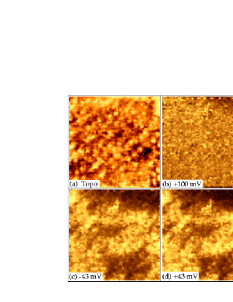
In Fig.1 we show a 150 nm x 150 nm topographic image and corresponding DOS maps at different tunneling voltages. The contrast in the topographic image corresponds to the apparent tip height as a function of its lateral position, whereas in the differential conductance maps the contrast represents a relative magnitude of the DOS at a given energy. Far beyond the superconducting gap () the DOS is uniformly distributed, as Fig.1b shows. At lower energies some contrast appears but near the gap edges the maximum contrast is found, representing the spatial distribution of the quasiparticle peak heights (Fig.1c for the occupied states side, Fig.1d for the empty states side of ). Bright zones in these images are areas in which the differential conductance has high quasiparticle peaks. These zones show the DOS having a superconducting shape, as in Fig.3a,b, and are therefore identified as ’superconducting’ areas. In very dark regions the peaks are absent, and the state density has a quite different shape (see Fig.3d). The form of the DOS we found in intermediate regions is shown in Fig.3c. Such a DOS is identical to the LTPG state density observed in films of Bi(2212) in our previous work [3]. In this Letter we continue to use the term LTPG for the spectrum having this particular form. Finally, the data in Fig.1 clearly indicate that the DOS is not homogeneously distributed over the surface, and superconducting regions are co-existing with non-superconducting ones. Exploring different locations of the sample we found similar large (100 nm and more) superconducting areas.
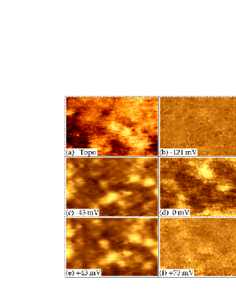
In other regions however, the superconducting DOS is not so dominant, and its variations are observed on a very small scale. In Fig.2 we present the 30 nm x 30 nm topographic image and corresponding DOS maps of such a typical region. Here the superconducting spectrum is present only in some locations, forming small islands (Fig.2c). The position and shape of these islands are precisely the same in the DOS maps at and . By analyzing the corresponding spectra along the points bordering the superconducting islands we find that they are surrounded by the peak-less LTPG state density (as in Fig.3c). The transitions from superconducting DOS to LTPG are spatially continuous, but take place on a very local scale of 1-3 nm. The analysis of numerous images indicated the existence of a smallest characteristic size of superconducting islands to be about 3 nm in diameter. No smaller areas with well-developed quasiparticle peaks in the DOS were found. Taking into account a relatively high Fermi velocity cm/sec reported in [12], the existence of such small superconducting regions suggests a very short interaction time of about sec.
The acquisition of a complete spectrum at each point of the image allows us to correlate unambiguously the DOS maps corresponding to different energies. In all images, the quasiparticle DOS maps for the energy fixed at the negative gap edge (as in Fig.1c, Fig.2c) perfectly correlate to those at the positive gap edge (Fig.1d and Fig.2d respectively). A rough correlation (a contrast reversal) is also found between the DOS maps taken at the gap edge and at zero energy, indicating that the zero-bias conductance is systematically smaller in superconducting regions as compared to LTPG ones. At the same time no contrast was found in DOS maps far beyond the gap edge for both positive and negative biases. In fact, any change in the DOS at the energy is directly observed in the differential conductance images . On the contrary, in topographic images, the feedback loop controls the tip height using the value of the tunneling current, which is proportional to the number of states integrated over the energy window . In our experiments the topographic images were taken at biases far beyond the gap value. Then, if the spectroscopic changes take place only near the gap edge, they will appear in such topographic images as a second order effect. The results in Fig.1 and Fig.2 confirm that the main DOS modifications take place essentially at the energies near the gap region, relevant to superconductivity. The conclusion is that the disorder perturbs the superconducting phase, and is not directly responsible for any new electronic states appearing in the underlying ’normal’ spectral density.
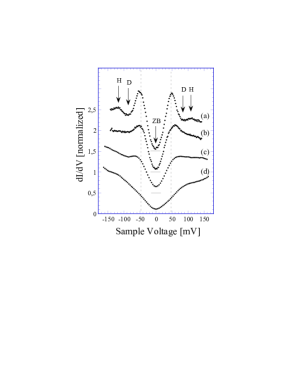
Let us analyse the state dynamics in the transition from superconducting to non-superconducting phase, as in Fig.3. Starting from the well-known superconducting DOS (Fig.3a) the very first effect is the removal of the spectral weight from the quasiparticle peaks. At the same time the dips/hump features vanish and the zero bias conductance slightly rises (Fig3c). At a first glance, there is no conservation of states in such a transformation, since the gap near the Fermi energy remains, and becomes even a bit larger [13]. Such a state dynamics in superconducting DOS - LTPG transition is surprisingly similar to the DOS variations observed in Bi(2212) single crystals in a magnetic field [6, 14]. In these experiments the superconducting DOS is almost homogeneously distributed over the surface, and modified only near the vortex cores. There also, the main effect is the suppression of the coherence peaks on a similar scale (2nm). In the case of Fig.2 however, the topology of the DOS variations is opposite to the vortex case: small superconducting clusters are immersed in a LTPG dominating medium. Further state dynamics is essentially to enlarge and broaden the LTPG. All sharp DOS structures disappear completely. Far away from superconducting regions, a wide and structure-less gap is often observed (Fig.3d). In terms of pair breaking, the effect would correspond to a strong suppression of the quasiparticle lifetime. Finally, the state dynamics in the superconducting DOS - LTPG transition we observe in single crystals of Bi/Pb(2212) is very similar to that previously reported in disordered thin films of Bi(2212). Therefore, it is a common effect in inhomogeneous superconducting cuprates.
In large superconducting regions the differential conductance spectra show sharp coherence peaks and well-developed dip/hump fine structure, whereas in the smallest superconducting islands the quasiparticle peaks are broader and dips/humps are suppressed. The tentative conclusion is then to associate the dip/hump signatures with a much larger characteristic scale. Their presence in the tunneling spectra could be a signature of a long range superconducting ordering.
The effect of disorder we observed in this work is different from the result of [15], in which Zn-containing single crystals of Bi(2212) were studied. At low concentration, Zn atoms, situated directly in Cu-O layers and acting as strong point defects, lead to the formation of bound states, locally observed. Although the quasiparticle peaks were found also suppressed near Zn-impurity, the main effect was a strong conductance peak, appearing near the Fermi energy. In Bi/Pb(2212) we did not observe such a peak, the main effect in the DOS being the local suppression of the quasiparticle peaks. It is not so surprising, since the role of Pb in Bi/Pb(2212) is very different from that of Zn. In this work the concentration of Pb atoms was chosen to be . At such a high density every fourth Bi atom is substituted by Pb in Bi-O layers, introducing a quasi-continuous weak disorder potential on the Cu-O layer. With respect to previously studied thin films of Bi(2212) [3], single crystals of Bi/Pb(2212) are much less structurally disordered, since Pb atoms substitute Bi ones without perturbing significantly the crystal structure. In this sense, Bi/Pb(2212) single crystals are much better described by a spatially varying degree of disorder.
To summarize, in this Letter the state dynamics in Bi/Pb(2212) single crystals is mapped energetically and spatially, giving a direct answer to recent theoretical considerations [1, 2]. It shows the differential conductance to be inhomogeneous over the sample surface on the nanometer scale. The minimum size of a superconducting island is estimated to be 3 nm, whereas the spectral changes take place on a slightly shorter scale (1-3 nm). Energetically these variations take place mainly within the range around the Fermi level. The spectral maps taken within this energy window correlate spatially, whereas they do not correlate to the topographic information. The effect is the consequence of the superconducting state - LTPG transition, due to the continuously varying disorder. The observed topology of the superconducting regions reveals the existence of two scales: a nanometer scale, on which the quasiparticle peaks in the DOS are formed/suppressed, and a larger scale associated with the appearance of sharp quasiparticle peaks and dip/hump structures. Intuitively, the first effect would correspond to a very local pairing, the second one reflecting a larger scale superconducting order.
We are grateful to J. Zasadzinski, J. C. Campuzano and B. Leridon for stimulating discussions, and F. Breton for his technical assistance.
REFERENCES
- [1] A. Ghosal et al., Phys. Rev. Lett. 81, 3940 (1998).
- [2] C. Huscroft and R. Scalettar, Phys. Rev. Lett. 81, 2775 (1998).
- [3] T. Cren et al., Phys. Rev. Lett. 84, 147 (2000).
- [4] Q. Huang et al. Physica C 161, 141 (1989).
- [5] I. Maggio-Aprile et al., Phys. Rev. Lett. 75, 2754 (1995).
- [6] Ch. Renner et al., Phys. Rev. Lett. 80, 3606 (1998).
- [7] P. Mallet et al., J. Vac. Sci. Techn. B, 14(2) (1996).
- [8] D. Mandrus et al., Nature 351, 460 (1991)
- [9] Ch. Renner and Ø. Fisher, Phys. Rev. B 51, 9208 (1995); Ch. Renner et al., J. Low Temp. Phys. 105, 1083 (1996).
- [10] P. Mallet et al., Phys. Rev. B 54, 13324 (1996).
- [11] N. Miyakawa et al., Phys. Rev. Lett. 80, 157 (1998); A. Yazdani et al., Phys. Rev. Lett. 83, 176 (1999)
- [12] A. Kaminski et al., cond-mat/0004482 (27 Apr.1998)
- [13] Since in STM the tunneling curves are normalized with respect to the tunneling resistance, one can not judge immediately on the absolute value of the DOS.
- [14] S.H. Pan et al., (2000), (submitted)
- [15] S.H. Pan et al., Nature 403, 746 (2000).