[
Charge noise analysis of an AlGaAs/GaAs quantum dot using transmission-type radio-frequency single-electron transistor technique
Abstract
Radio-frequency (rf)- operated single-electron transistors (SETs) are high-sensitivity, fast-response electrometers, which are valuable for developing new insights into single-charge dynamics. We investigate high-frequency (up to 1 MHz) charge noise in an AlGaAs/GaAs quantum dot using a transmission-type rf-SET technique. The electron capture and emission kinetics on a trap in the vicinity of the quantum dot are dominated by a Poisson process. The maximum bandwidth for measuring single trapping events is about 1 MHz, which is the same as that required for observing single-electron tunneling oscillations in a measurable current (0.1 pA).
]
A single electron transistor (SET) is a high-sensitivity electrometer that measures a small fraction of the elementary charge, , on a small island [1]. If the island, or quantum dot atom, shows well-defined eigenstates in a zero-dimensional confinement potential, quantum mechanical effects found in atomic physics can be reproduced with tunable parameters [2]. The ability to control single-particle quantum states will be helpful for developing quantum logic gates [3, 4, 5]. So the dynamical behavior of charge states need to be studied for those interested. Most of the experiments have been done by taking the dc response from an ac modulation. However, direct measurement of the ac response of a single-particle state has not been done due to technical difficulties. Recently, a radio-frequency (rf) operated SET technique for following the fast response of the charge has been proposed and demonstrated by R. J. Schoelkopf et al. [6] . A bandwidth greater than 100 MHz would be useful for studying single-electron dynamics such as single-electron tunneling oscillation [7] and coherent charge oscillation [5], as well as for various sensors [8].
In this letter, we describe an application of the rf-SET for detecting individual emission and capture events of a trap in a semiconductor. A modified rf-SET technique that measures the transmission of rf signals through a resonator, is also used for a quantum dot fabricated in an AlGaAs/GaAs heterostructure [9]. The charge noise of the quantum dot is studied both for low-frequency noise and for random telegraph signals (RTSs) originating from a trap near the dot. For a specific RTS, the statistics of the electron capture and emission are given by the Poisson process.
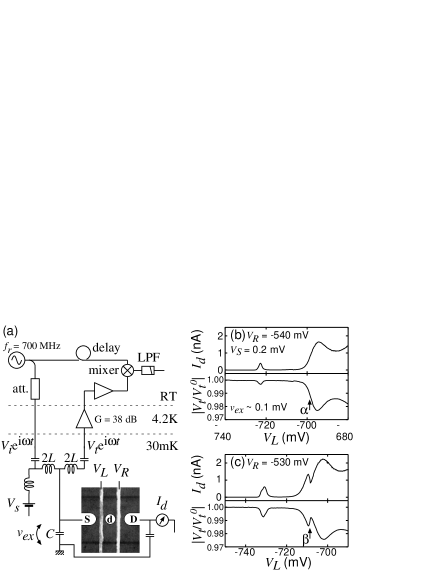
The transmission-type rf-SET technique is shown schematically in Fig. 1(a). The SET, or quantum dot, is fabricated in an AlGaAs/GaAs modulation doped heterostructure using focused ion beam implantation and patterning of fine Schottky gates [10]. The two gate voltages, and , control the two tunneling barriers independently, and effectively lift the electrostatic potential of the dot. The SET is placed in an LC resonator (two inductors of 2 and one capacitor of ). Other lumped elements allow measurement of the dc current and rf-transmission simultaneously. When the rf carrier signal is supplied at the resonant frequency, , to the resonator, a transmitted signal appears at the other end of the resonator. The transmitted signal is sensitive to the resistance, , of the SET [11], or the charge on the island, , i.e., for and , where = 50 is the cable impedance and is the quality factor of the resonator. The rf excitation voltage across the SET, , is given by .
Compared with the reflection-type rf-SET originally demonstrated in Ref. REFERENCES, the transmission-type rf-SET has some advantages for convenient measurements. Since the incident and the transmitted signals are separated, a directional coupler necessary for the reflection measurement is not required (although two inductors are necessary for the transmission measurement). The transmission signal always shows a clear and sharp resonance signal when the frequency is swept, while the reflection signal does not particularly if the sample is highly resistive or Coulomb blockaded. Once the frequency is adjusted properly, both transmitted and reflected signals behave similarly if the sample resistance is high, . High-sensitivity[12] and high-frequency (ideally upto ) operation of the rf-SET could also be applied to the transmission-type rf-SET.
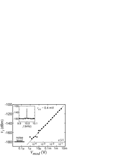
Figure 1(b) shows typical Coulomb blockade oscillations measured by dc current (upper trace) and rf-transmission (lower trace). The traces are taken simultaneously with a dc bias voltage of = 0.2 mV and an rf excitation of 0.1 mV (rms for all ac amplitudes). The best charge sensitivity is obtained at the largest slope, , denoted by the arrow labelled by in the figure. We estimate the charge sensitivity, i.e., the minimal detectable charge on the island, by applying a sinusoidal modulation to the as follows. The inset of Fig. 2 shows the frequency spectrum of transmitted signal at the modulation frequency, = 10 kHz. The signal intensity is linearly dependent on the modulation amplitude, , as shown in Fig. 2. We obtain a charge sensitivity of at an excitation of 0.4 mV. This is larger than the thermal noise and the shot noise, but is dominated by the noise of the amplifier.
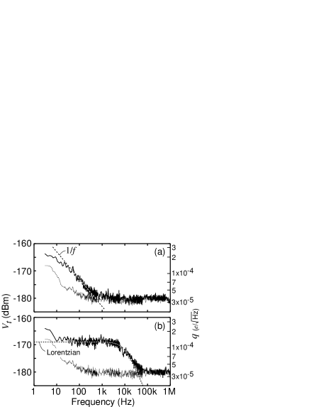
Figure 3(a) shows the spectra of the transmitted signal. The thick trace measured at the best charge sensitivity ( in Fig. 1(a)) shows the SET noise, while the thin trace measured at zero conductance of the SET shows the noise of the measurement system. The SET shows noise below 1 kHz, similar to that reported in metal SETs [6, 13]. For frequencies above 1 kHz, the white noise is dominated by the HEMT amplifier. Better amplifiers and a higher resonator should reduce the system noise.
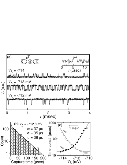
We also find a RTS in our dot. The specific trap we study has a relatively fast switching time and is a good example for demonstrating the fast response of the rf-SET. Figure 1(c) shows another CB oscillation with a jump seen at about -710 mV, labelled in the figure, where the jump appears at the largest of the CB peak for the best sensitivity. The jump is caused by the emission and capture of an electron from a trap in the vicinity of the quantum dot. The trap may be a defect in the crystal or a potential hollow (maybe a quantum dot) unintentionally created during fabrication. This specific trap is located close to the left gate rather than the right gate (schematically shown in the left inset of Fig. 4(a)) [14].
The RTS noise is observed on a relatively short time scale for this particular trap, as shown in Fig. 4(a). The emission and capture statistics are derived from the RTS noise in the time domain. The duration time for the trap being empty (lower signal in the figure) corresponds to the capture rate, and the duration time for the trap being occupied (higher signal) corresponds to the emission rate. These durations are widely distributed, as shown in Fig. 4(b), and well characterized by an exponential dependence, , with time constant . The mean () and the standard deviation () of the durations are practically the same as . These observations indicate a Poisson process, i.e., each emission and capture process is an independent event [15]. The time constant for capture, , and emission, , are strongly dependent on the energy level of the trap, , or on the gate voltage (see Fig. 4(c)). Simply assuming a constant attempt rate for both transitions, , and a Fermi distribution, , in the source electrode, the capture and emission rates should be given by and , respectively. The measured time-constants are reproduced with parameters 12 s and = 0.46 meV, as shown by the solid lines in Fig. 4(c). The effective temperature, , is comparable to the rf excitation voltage across the SET, 0.4 mV. We find that increases with .
The power spectrum of the RTS noise (Fig. 3(b)) is flat up to a few kHz and decreases above 5 kHz. The spectrum can be fitted with a Lorentzian curve (dashed line), . The fitting parameter, = 16 sec, is comparable to from the time domain analysis, which also indicates a Poisson process.
The RTS noise has been studied in sub-micrometer Si metal-oxide-semiconductor structures [15], AlGaAs/GaAs narrow channels [16], and quantum dots [17]. A higher sample resistance in general restricts the lower frequency range that can be measured. Thus, most of the measurements on SETs ( 26 k in principle) are restricted to the noise region [13]. Our observation of RTS in the quantum dot is consistent with those previously reported. The maximum bandwidth , where the change in the charge, , is distinguished from the noise, , is given by . This yields 1 MHz for the trap we investigated. We observe a duration as short as few and rise/fall time shorter than 1 (the right inset of Fig. 4(a)), when the bandwidth is set to 2.5 MHz. If the trap is replaced with another quantum dot connecting another set of leads [18], single electrons will tunnel through the dot with a frequency of (600 kHz at a driving current, , of 0.1 pA). The rf-SET should resolve each tunneling event of such a current.
In summary, we have demonstrated a transmission-type rf-SET using a quantum dot for detecting charge kinetics of a trap in an AlGaAs/GaAs heterostructure. Our results are encouraging for the direct measurement of ac response from a single-electron state.
We thank D. G. Austing, R. Espiau de Lamaestre, A. Kanda, S. Komiyama, B. Starmark for their discussion and help.
REFERENCES
- [1] “Single Charge Tunneling, Coulomb Blockade Phenomena in Nanostuctures” ed. H. Grabert and M. H. Devoret, NATO ASI series B 294.
- [2] For a review, see L. P. Kouwenhoven et al., in ”Mesocopic Electron Transport” ed. L. L. Sohn, L. P. Kouwenhoven, and G. Schön, NATO ASI series E 345, pp. 105-214.
- [3] D. Loss and D. P. DiVincenzo, Phys. Rev. A 57, 120 (1998).
- [4] T. H. Oosterkamp, T. Fujisawa, W. G. van der Wiel, K. Ishibashi, R. V. Hijman, S. Tarucha, and L. P. Kouwenhoven, Nature 395, 873 (1998).
- [5] Y. Nakamura, Yu. A. Pashkin and J. S. Tsai, Nature 398, 786 (1999).
- [6] R. J. Schoelkopf, P. Wahlgren, A. A. Kozhevnikov, P. Delsing, and D. E. Prober, Science 280, 1238 (1998).
- [7] D. V. Averin and K. K. Likharev, J. Low Temp. Phys. 62, 345 (1986).
- [8] R. J. Schoelkopf, S. H. Moseley, C. M. Stahle, P. Wahlgren, and P. Delsing, IEEE Trans. Appl. Supercond., 9, 2935 (1999).
- [9] T. Fujisawa and Y. Hirayama, Japn. J. Appl. Phys. 39, 2338 (2000).
- [10] T. Fujisawa and S. Tarucha, Appl. Phys. Lett. 68, 526 (1996); Superlattices Microstruct. 21, 247 (1997); Japn. J. Appl. Phys. 36, 4000 (1997).
- [11] The SET consists of tunneling resistance and capacitance, whose values can be deduced from the phase analysis of the transmitted signal. We focus here on the region where the resistance change of the SET is dominant.
- [12] A. N. Korotkov and M. A. Paalanen, Appl. Phys. Lett. 74, 4052 (1999).
- [13] B. Starmark, T. Henning, T. Claeson, and P. Delsing, J. Appl. Phys. 86, 2132 (1999).
- [14] The location of the trap can be estimated from the gate-voltage dependence, as reported in Ref. [17]. The energy state of the trap is tunable with . The trap is occupied by an electron for -710 mV and is empty for -710 mV. The trapping of an electron lifts the potential of the dot by 0.3 meV, or induces an equivalent charge of 0.1 on the dot, and changes (about 20%) the resistance of the tunneling barriers.
- [15] M. J. Kirton and M. J. Uren, Adv. Phys. 38, 367 (989).
- [16] F. Liefrink, J. I. Dijkhuis, and H. van Houten, Semicond. Sci. Technol. 9, 2178 (1994).
- [17] T. Sakamoto and K. Nakamura, Appl. Phys. Lett. 68, 2861 (1996).
- [18] D. S. Duncan, C. Livermore, R. M. Westervelt, K. D. Maranowski, and A. C. Gossard, Appl. Phys. Lett. 74, 1045 (1999).