[
ARPES study of Pb doped - a new Fermi surface picture
Abstract
High resolution angle resolved photoemission data from Pb doped (Bi2212) with suppressed superstructure is presented. Improved resolution and very high momentum space sampling at various photon energies reveal the presence of two Fermi surface pieces. One has the hole-like topology, while the other one has its van Hove singularity very close to , its topology at some photon energies resembles the electron-like piece. This result provides a unifying picture of the Fermi surface in the Bi2212 compound and reconciles the conflicting reports.
]
The Fermi surface plays an important role in understanding the physics of any material. Among other things its shape and size determine the type and number of charge carriers in the material as well as the charge and spin dynamics. For example, in the context of the Fermi liquid approach to high temperature superconductors (HTSCs), Fermi surface topology is related to commensurate or incommensurate nature of the neutron data [1]. Furthermore, detailed knowledge of the Fermi surface is essential to determine the superconducting gap size and symmetry in the superconducting state.
Angle resolved photoemission spectroscopy (ARPES) is a unique tool to probe the Fermi surface of the HTSCs. Over the last decade the HTSC system most extensively investigated by ARPES is Bi2212 [2, 3, 4, 5, 6, 7, 8, 9, 10]. However, the existence of superstructure in the layer and shadow bands has made the Fermi surface determination in this compound complicated, especially around the point, where main bands, superstructure bands, and shadow bands cross the Fermi level. For several years there was a general agreement for a hole-like Fermi surface centered around , mainly based on ARPES experiments performed at photon energy [4, 5, 6, 7, 8, 9, 10]. This hole-like Fermi surface picture was believed to apply over the entire doping range studied by ARPES (from underdoped samples with to overdoped samples with ). Later a vigorous discussion started, with experiments utilizing photon energy suggesting an electron-like Fermi surface centered around the point [11, 12, 13]. Other groups disputed electron-like Fermi surface reports, dismissing the observed results by invoking the interplay of matrix element effects with layer superstructure and shadowbands [14, 15, 16, 17]. Finally, recent reports on Bi2212 using 22 eV photons demonstrated the presence of the two Fermi surfaces in the material due to bonding and antibonding interaction of CuO planes [18, 19]. It is of great importance to reconcile all the reported results and to resolve the uncertainty in the Fermi surface of Bi2212 - the compound extensively studied and the source of many significant results.
Because the main discrepancy originates in the region, where the superstructure effect of the layer is strongest, a definitive resolution of the Fermi surface issue can be found by studying the Pb-doped Bi2212 system. In this compound Pb is doped into the plane disrupting the plane modulation and removing the superstructure complication near the region [16, 17, 20].
In this Letter we present results of Fermi surface mapping of Pb-doped Bi2212 with high energy resolution and very high space sampling. We used various photon energies and different methods to determine the Fermi surface. Our 22 eV data complement recent reports on the existence of two Fermi surface pieces. The photon energy dependence reveals that the relative intensity depends strongly on photon energy. While the bonding Fermi surface has a clear hole-like topology, the antibonding piece has its van Hove singularity very close to and its Fermi surface is electron-like as seen at some photon energies. This result contradicts earlier reports of a single universal Fermi surface in this compound [8, 16, 17]. On the other hand our data provides a unifying foundation for understanding the controversies about the Fermi surface of this important superconductor, as different reports stress different aspects of the global Fermi surface features.
ARPES data have been recorded at beamline of the Advanced Light Source utilizing and photon energy in vacuum. The sample was kept in the fixed position relative to the beam polarization, and the analyzer was rotated. The beam polarization was in the sample plane perpendicular to direction, with beam nearly at grazing incidence with the sample surface. We used a Scienta SES 200 analyzer in the angle mode, where cuts parallel to direction are carried out. The momentum resolution was in the scan direction and in the perpendicular direction for 55 eV photon energy and better for other energies, and the energy resolution was . An extensive and fine sampling mesh with more than 4000 EDCs for each photon energy was collected. The slightly overdoped Pb-doped Bi2212 () and overdoped Pb-doped Bi2212 () were grown using the floating-zone method. The single crystalline samples were oriented by using Laue diffraction ex situ and cleaved in situ in vacuum. The samples were measured at 100K (Fig. 1,2 and 4) and 20K (Fig. 3). The Fermi energy was obtained from the EDCs of polycrystalline .
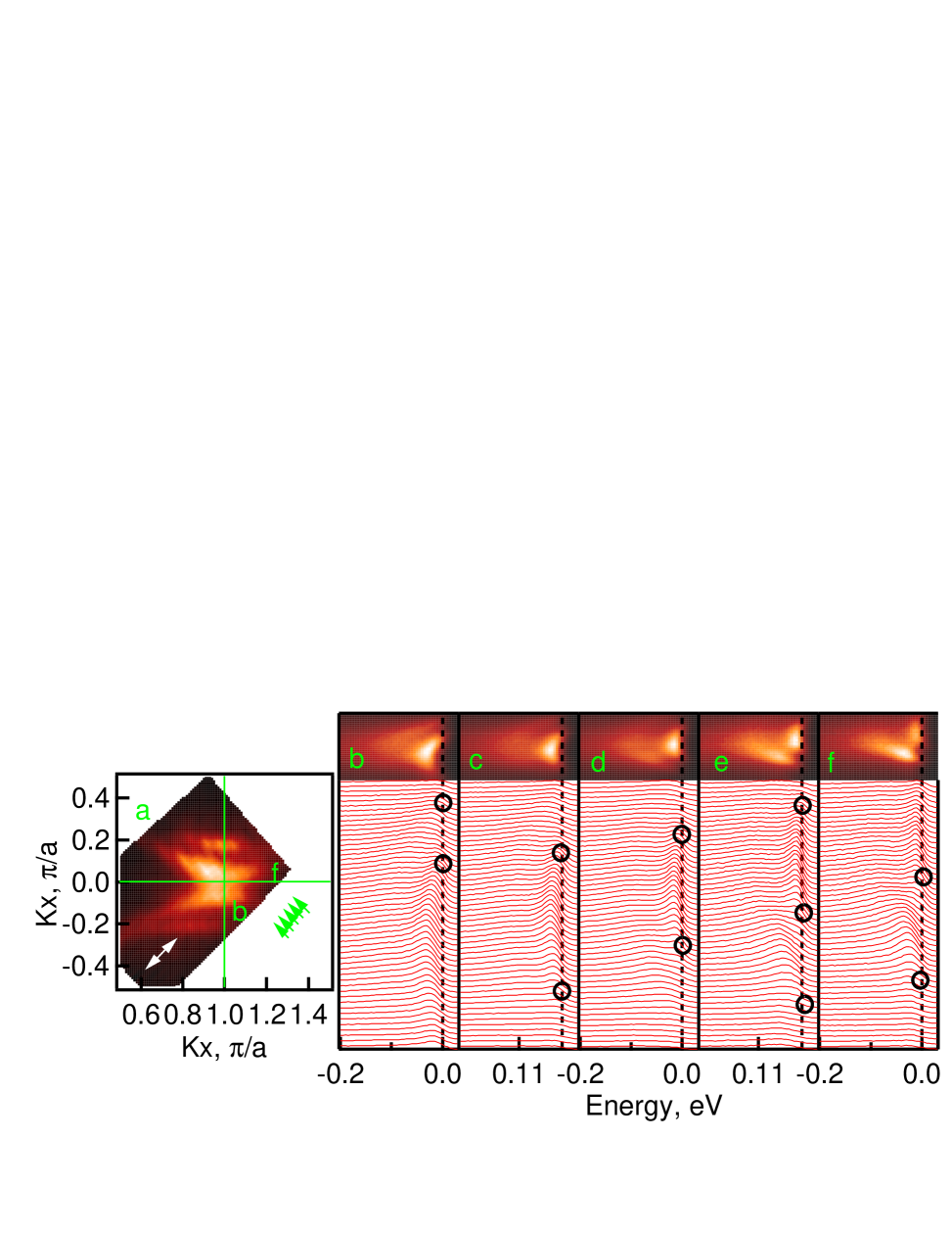
In panel a) of Fig. 1 we show the map of spectral intensity at Fermi energy () obtained at 22 eV photon energy. The white arrow shows the polarization of radiation with respect to the crystal surface. To determine the spectral intensity map we divide each EDC by the integrated signal intensity from a 100 meV window above the , which comes from higher order synchrotron light and is proportional to photon flux. The normalized EDCs represent electron spectral function weighted by the Fermi function and matrix element[21]. Highest intensity points in the spectral intensity map at the Fermi energy give one method for determining Fermi surface. In panels 1b)-1f) we plot raw EDC data obtained along select cuts shown in panel a) by green arrows. Here Fermi surface crossing is defined as the location in the momentum space where the intensity of the spectral feature decreases drastically and the leading edge crosses the Fermi level. From both the near spectral weight image plot and from the EDCs one clearly sees two Fermi surfaces, as indicated by solid ovals in panels b to f. Concomitant presence of two Fermi surface pieces is consistent with recent data recorded at a similar photon energy [18, 19]

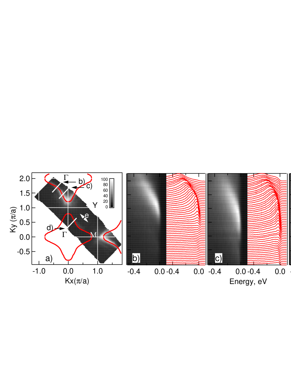
Fig. 2a) shows 22 eV data from another sample taken in a more extended k-space area. This data were taken at 20K in the superconducting state, where the spectral weight around M point is suppressed at the Fermi level due to the sc gap opening, so the map shown corresponds to 12 meV BE. This map can effectively be used to indicate the underlying Fermi surface. Although the maximum gap is larger than the energy window, finite resolution still reveals the underlying Fermi surface, and larger integration window does not change the picture. This data, as well as the normal state data in panel a) of Fig. 1, show striking resemblance to theoretical simulation by Bansil et al. [22] for the same photon energy and polarization, as shown in panel b). The simulation uses first-principles one-step photoemission model calculation and comes up with two bands for two adjacent planes in a unit cell. These two bonding and antibonding bands give rise to two Fermi surfaces. The bonding piece is an outer hole-like piece, indicated by blue lines in the inset of panel a). On the other hand the antibonding piece, indicated by the red area in the inset of panel a), is hard to judge from these data, because the saddle point of the band is very close to at [23]. The simulation also indicates that the image plot is very similar whether this piece of the Fermi surface is hole-like or electron-like, i.e. whether the Van Hove saddle point is above or below . The absence of superstructure complication in our data and the striking similarity between experiment and theory strongly suggest that there are indeed two pieces of the Fermi surface in Pb Bi2212.
The Fermi surface seen under other measurement conditions turns out to be very different. Fig. 3 shows data recorded at 55 eV under the same measurement geometry. Panel a) shows the map of spectral intensity at in the momentum space. In panels b), c) and d) we plot raw data obtained along the select cuts shown in panel a) by thick white lines. Cut b) is close to the nodal direction in the second Brillouin zone, while cuts c) and d) are cuts equidistant from point. The sampling density in the cuts is very high and is representative of the sampling density of the entire k-space studied. The high quality data clearly shows a quasiparticle dispersing towards the Fermi level, eventually crossing it and disappearing. While the intensity map in panel a) hardly shows any features in the first zone, panel d) clearly shows a well-resolved feature crossing the Fermi level, similar to panel c), with the overall intensity a factor of 10 lower than that in panel c). In fact, all features seen in the second zone are observed in the first zone as well. The Fermi surface shape emerging for this photon energy is electron-like. We have confirmed this result with data taken in all three Brillouin zones by using three complimentary methods: intensity map at , the traditional method of tracking the EDCs, and the sharpest drop in . The contrast in data from Figures 1-3 immediately suggests that the 55 eV data picks out the inner piece of the Fermi surface.
To investigate the photon energy dependence of the FS further, we collected data at other photon energies and in Fig. 4 we plot the measured spectral intensity maps at . In panel a) we plot our spectral intensity map collected at 27 eV. We see an electron-like FS in the first zone, and the spectral weight in the second zone is significantly suppressed. This complements the 55 eV data in panel d). In panel b) at 33 eV photon energy spectral intensity map shows strong suppression of the spectral weight at the M point and can be interpreted as either hole-like and electron-like. This data is quite different from earlier results recorded at another geometry [10, 11, 12]. 44 eV data in panel c) looks very similar to 22 eV data in panel a) with bilayer split Fermi surfaces. Spectral weight map FS results are supported by individual EDC analysis.
There’s a very unusual photon energy related variation in the ARPES data. With the large unit cell size in the normal direction (), one would expect periodicity with 1-2 eV steps in photon energy for the energy range studied. Surprisingly, this is not the case. Existence of bilayer split Fermi surface means strong interaction between the two planes in Bi2212 unit cell. It is reasonable to assume that the variation in the data with the photon energy is also driven by the separation of the layers , with corresponding . This would be more consistent with the observed variations with large photon energy intervals. Calculations similar to [22] for a range of photon energies will be very useful to understand this phenomena.

Our results, in particular the variation of the Fermi surface picture with photon energies and the observation of the bilayer splitting, contradict earlier reports from Pb doped Bi2212. Previous data [16, 17] from the same material at different photon energies were interpreted as an evidence for the universal hole-like Fermi surface. We attribute this discrepancy mostly to poorer energy (70 meV compared to ours 7-18 meV) and momentum ( compared to ours ) resolution used in that study for photon energies other then 22.4 eV. Attempts were also made to support a single universal hole-like Fermi surface picture by invoking matrix element arguments[14, 15]. While a band calculation did show a strong spectral intensity variation with photon energy [22], it is not applicable to Fermi surface determination at a particular photon energy. What really matters is the matrix element variation in a small region in the same Brillouin zone, which is actually small [22]. The unambiguous evidence for two Fermi surface pieces show the matrix element argument for single universal hole-like Fermi surface to be misleading and incorrect.
The polarization setup used in our experiment is favorable for observing the bilayer splitting [22]. Observation of the splitting of the bands due to the interaction between the layers was a long standing problem. Earlier photoemission results were interpreted as evidence for the absence of the bilayer splitting [8]. Our data in Fig. 1, 2 and 4, collected with much better energy and momentum resolution, show the splitting to be present, even for the samples with Tc not far from optimal.
The picture emerging from the above is clear: there are two pieces of the Fermi surface, one of them clearly hole-like. The other piece is different, as it lies very close to the special point where Fermi surface changes from hole-like to electron-like with small change in chemical potential or . This is the underlying reason for this piece to behave slightly differently at different photon energies. This picture provides a unifying foundation for all the controversial reports on the FS shape in Bi2212. Bi2212 Fermi surface has always been attributed to the plane, and because doping with Pb does not change the plane, the Fermi surface in Pb-doped and Pb-free compounds should be the same. Our finding indicates that the accepted picture of a single hole-like Fermi surface in Bi2212 for the entire doping range studied is incorrect. Instead, there exists another Fermi surface piece that is at the boundary between hole and electron character.
We would like to thank J. D. Denlinger for the help with data analysis software. The experiment was performed at the Advanced Light Source of Lawrence Berkeley National Laboratory, supported by DOE’ Office of Basic Energy Science, Division of Materials Science with contract DE-AC03-76SF00098. The Stanford work was supported by NSF grant through the Stanford MRSEC grant and NSF grant DMR-9705210. The SSRL’s work was also supported by the Office’s Division of Materials Science.
REFERENCES
- [1] M. R. Norman, preprint, cond-mat / 9912203
- [2] C. G. Olson et al., Science 245, 731 (1989)
- [3] D. Dessau et al., Phys. Rev. Lett. 71, 2781 (1993)
- [4] P. Aebi et al., Phys. Rev. Lett. 72 2757 (1994)
- [5] Jian Ma et al., Phys. Rev. B 51, 3832 (1995)
- [6] A. G. Loeser et al., Science 273, 325 (1996)
- [7] P. J. White et al., Phys. Rev. B 54, 15669 (1996)
- [8] H. Ding et al., Phys. Rev. Lett. 76, 1533 (1996)
- [9] M. R. Norman et al., Nature 392, 157 (1998)
- [10] N. L. Saini et al., Phys. Rev. Lett. 79, 3467 (1997)
- [11] Y. -D. Chuang et al., Phys. Rev. Lett. 83, 3717 (1999).
- [12] D. L. Feng et al., preprint, cond-mat / 9908056.
- [13] A. D. Gromko et al., preprint, cond-mat / 0003017.
- [14] H. M. Fretwell et al., Phys. Rev. Lett. 84, 4449 (2000)
- [15] J. Mesot et al., preprint, cond-mat / 9910430.
- [16] S. V. Borisenko et al., Phys. Rev. Lett. 84, 4453 (2000)
- [17] S. Legner et al., preprint, cond-mat / 0002302.
- [18] D. L. Feng et al., cond-mat/0102385
- [19] Y. -D. Chuang et al., cond-mat/0102386
- [20] P. Schwaller et al., J. Elec. Spec. Rel. Phen., 76 127 (1995).
- [21] S. Hufner, Photoemission Spectroscopy, Springer-Verlag, New York, (1995)
- [22] A. Bansil et al., Phys. Rev. Lett. 83 5154 (1999).
- [23] A. Bansil et al., private communication