Coulomb blockade in one-dimensional arrays of high conductance tunnel junctions
Abstract
Properties of one-dimensional (1D) arrays of low Ohmic tunnel junctions (i.e. junctions with resistances comparable to, or less than, the quantum resistance k) have been studied experimentally and theoretically. Our experimental data demonstrate that – in agreement with previous results on single- and double-junction systems – Coulomb blockade effects survive even in the strong tunneling regime and are still clearly visible for junction resistances as low as 1 k. We have developed a quasiclassical theory of electron transport in junction arrays in the strong tunneling regime. Good agreement between the predictions of this theory and the experimental data has been observed. We also show that, due to both heating effects and a relatively large correction to the linear relation between the half-width of the conductance dip around zero bias voltage, , and the measured electronic temperature, such arrays are inferior to those conventionally used in the Coulomb Blockade Thermometry (CBT). Still, the desired correction to the half-width, , can be determined rather easily and it is proportional to the magnitude of the conductance dip around zero bias voltage, . The constant of proportionality is a function of the ratio of the junction and quantum resistances, , and it is a pure strong tunneling effect.
1 Introduction
The effect of Coulomb blockade in 1D arrays of normal tunnel junctions can be used for absolute thermometry [1]-[3]. The properties of such arrays have been extensively investigated both experimentally and theoretically [1]-[4]. In all these works arrays of high Ohmic junctions with the junction resistances, , higher than or of the order of the quantum resistance k have been studied. In this limit a theoretical description of the Coulomb blockade is well developed [5] and it has been successfully applied [1]-[3] to explain experimental findings in the high temperature regime, , where is the capacitance of a single junction.
From the practical point of view, large () 1D arrays used as thermometers are advantageous over the smaller ones, because of higher accuracy of temperature measurements. At the same time, increasing the number of junctions in the array obviously yields an increase of its total resistance . Since in practice it is desirable to avoid very large values of , it appears natural to relax the condition and consider 1D arrays of relatively highly conducting tunnel junctions with of the order of or smaller. A natural way to avoid this is the parallel connection of several 1D arrays, and this is used extensively in Coulomb blockade thermometry (CBT). To avoid a large total number of junctions, a more straightforward solution would be to decrease the resistance of each individual junction. On the other hand, heating effects turn out to be much more pronounced for highly conducting junction arrays [6]. Hence, from this point of view, it is better not to decrease down to very low values.
The above considerations motivated us to investigate the interplay between Coulomb blockade and strong tunneling effects in 1D arrays of normal metallic tunnel junctions. Do Coulomb blockade effects survive if the junction resistance becomes smaller than the resistance quantum? Both theory [7]-[11] and experiment [12]-[15] give a clear positive answer to this question. An adequate theoretical approach which enables one to study electron transport in the strong tunneling regime is well established [16, 8]. This so-called quasiclassical Langevin equation technique allows to proceed analytically and remains accurate at not very low temperatures and/or voltages [8]:
| (1) |
for , and otherwise. The condition (1) implies that in the strong tunneling regime , which is of a primary interest for us here, the technique [16, 8] covers practically all experimentally accessible values of temperature and bias voltage. In several previous publications [8]-[11], the Langevin equation technique was applied to analyze the Coulomb blockade and strong tunneling effects in single junctions and SET transistors, where the curves were derived at arbitrary tunneling strength. The results of this theoretical analysis turned out to be in good agreement with available experimental data [12, 13, 15].
The structure of the paper is as follows: In Section 2 we develop a theoretical analysis of Coulomb blockade effects in 1D tunnel junction arrays in the strong tunneling regime. In Section 3 we present experimental results obtained for the arrays with resistances in the range k and compare these results with our theoretical predictions. Our main conclusions are summarized in Section 4.
2 Theory
In order to theoretically study the behavior of low resistance tunnel junction arrays we are going to use the technique of quasiclassical Langevin equation developed in Refs. [16, 8]. In this section we generalize the approach presented in [8] to the case of 1D arrays of tunnel junctions.
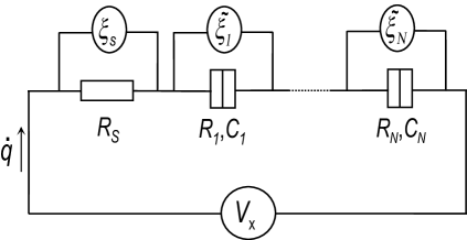
We consider an array of normal metal tunnel junctions in series (Fig. 1). The system can be described by the following Langevin equations [8]-[11]:
| (2) | |||||
Here is the effective phase and is the resistance of the electromagnetic environment. The shot noise of the -th junction depends on as [16, 8]:
| (3) |
Here are Gaussian stochastic variables with the following pair correlators:
| (4) | |||||
In Eqs. (4) we have defined
| (5) |
where stands for the principal value. There exist no correlations between the noise terms from different junctions: for .
Averaging Eqs. (2) over the noise realizations (we will denote this average by angular brackets), we obtain the general expression for the current in the array:
| (6) |
where is the total resistance of the array. These two equations define the curve of the chain.
The problem, now, reduces to the evaluation of the noise averages . In order to do this, we first exclude the current from the equations (2) and get the following ones for the phases :
| (7) |
Then we define the small deviations of the phase and the shot noise from their average values and , respectively. They obey the following equations
| (8) |
Applying the Fourier transformation and solving the corresponding equations, we find
| (9) |
where is the total impedance seen by the -th junction and the functions describe the mutual influence of the junctions on each other. Equation (9) applies to any array of tunnel junctions of any dimensionality. In the case of 1D arrays from Eq. (8) we find
| (10) |
Here we do not present the expressions for the functions because, as we will see below, the contribution of corresponding terms turns out to vanish. We find
| (11) | |||||
where the response function is defined as
| (12) |
and are defined analogously.
It is important to emphasize that Eqs. (9) and (11) are not the explicit solutions for the phase, but the integral equations. The variables on the right hand side of these equations depend on through the and terms in the shot noise (3). These integral equations can be solved by iteration. Here we restrict ourselves to the first iteration and put in the right hand side of Eq. (11).
The next step is to evaluate the average values which enter the expression for the current (6). We make the following approximation:
Here is the average voltage on the -th junction. Making use of Eq. (11) we get
| (13) |
Here we note that the terms containing the kernels do not contribute to the result because there exists no correlation between the noise on different junctions. Now the current is expressed as follows:
| (14) |
Let us first assume that all the junctions in the chain are identical, i.e. they have the same resistance and the same capacitance . Then we get
| (15) |
| (16) | |||||
The current (14), then, can be found exactly:
| (17) |
Here , , , and
| (18) | |||||
In the limit the final result of the above expressions reduces to that of our previous analysis [9].
The differential conductance is given by the following equation
| (19) | |||||
Now let us put and consider the high temperature limit .
Then, in the first order in , we find
| (20) | |||||
and
| (21) |
This result exactly coincides with that found for the high Ohmic junctions [1, 3].
Equation (21) is basic for the Coulomb blockade thermometry. The half-width of the dip in the is related to the temperature as [1]. This relation is proven to be very accurate for the high Ohmic arrays. To estimate its accuracy in the strong tunneling limit, we use the expression (19), put and numerically solve the following equation
| (22) |
Here is the normalized half-width, . The solution of this equation is plotted in Fig. 2.
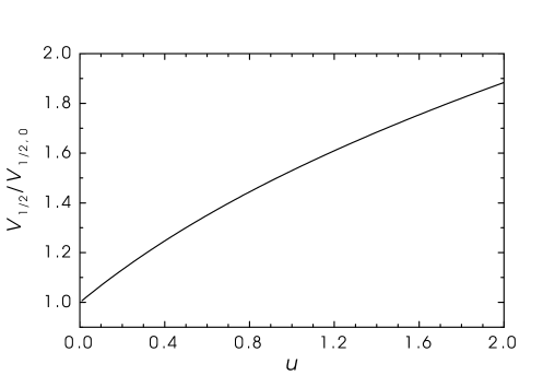
In the limit of high temperatures (small ) we find
| (23) |
The zero bias conductance can be obtained from Eq. (19):
| (24) |
Here , and is the Euler’s constant. Note that the result (24) is equivalent to the one recently derived within the framework of a linear response approach based on the Kubo formula [17]. At high temperatures (small ) we find from (24)
| (25) |
Now we will study the effect of the junction asymmetry on the properties of the thermometer. If the junctions are not identical, the equations become more complicated. Here, we will consider only the high temperature limit. In this limit the function decays at short times of order , and one can replace the response function in the integral (14) by its short time expansion, which starts from the linear-in-time term, . Then we get
| (26) |
| (27) |
Here and . From Eqs. (12) and (15) we find
| (28) |
Assuming that deviations, and , of the junction parameters from the reference values and are small, we expand Eq. (27) in powers of and up to the second order. Then we get
| (29) | |||||
Here
and
| (30) | |||||
We observe that is zero if the deviations of all the resistances are equal to each other. We also note that the terms linear in vanish in the sum and, as a consequence, in Eq. (29). Both these properties reflect the fact that the half-width depends only on temperature if the resistances of all the junctions are the same. Now the correction to the half-width of the conductance dip can be obtained peturbatively in and . In the first non-vanishing order we get
| (31) | |||||
where .
3 Experiment
To obtain suitable data for comparison between the theoretical predictions (presented in the previous section) and the experiment, we fabricated high conductance Al/AlOx/Al tunnel junction arrays by electron beam lithography and two-angle shadow evaporation techniques. As a substrate, we used nitridized silicon wafers. The number of junctions in the array, , was twenty, and each junction had an area of about 0.025 m2. Different high conductance samples with per-junction asymptotic resistances of k, together with two samples with lower conductances (in the intermediate regime) with per-junction resistances equal to 20 k and 23 k, were made and measured. In order to decrease heating effects in the high conductance arrays at higher bias voltages, the islands between the junctions in most of the samples (albeit not for those shown in Fig. 3) were made sufficiently large with cooling bars (see, e.g., [6]) attached to them. The measurements were carried out in the temperature range 1.5 K 4.5 K, i.e. at temperatures of liquid helium. To measure the temperatures as accurately as possible, we fabricated CBT sensors on the same sample stage in the vicinity of the samples to be measured.
As it was already discussed above, Coulomb blockade – although weakened – is not smeared out completely even in the strong tunneling limit. The zero bias conductance of the array is always lower than its asymptotic value at high voltages. In general, the zero bias conductance at high temperatures can be written as
| (32) |
In the limit of strong tunneling, , from Eq. (25) we find while in the opposite weak tunneling limit the approach based on the Master equations, [2], yields Here, as before, is the (per-junction) resistance of the homogeneous array at large bias voltages.
In the intermediate regime, which is appropriate for most of the arrays measured in the experiment, one can conjecture that . Previously, this conjecture was verified for the specific case of SET transistors () [11, 18].
Within the first order in , the inverse resistance enhancement at zero bias voltage, , where , can be easily derived from Eq. (32) as:
| (33) |
where, according to the theory,
| (34) |
and
| (35) |
The expression above has two characteristic features: linearity in and dependence of its slope on the capacitance of the junctions in the array. In addition, this equation predicts an offset which depends only on the number of junctions in the array, and on the ratio of the quantum and per-junction resistances. Below, while making comparison between the measured data and the predictions of Eq. (33), we will take the the weak tunneling correction into account, i.e, .
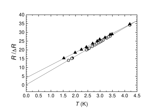
The value , measured for two tunnel junction arrays with and at different temperatures, is displayed in Fig. 3. The asymptotic resistances of the samples were 23 k (open circles) and 1.2 k (solid triangles). One observes an almost perfect linear dependence of the value on temperature (cf. Eq. (33). This dependence can be used to obtain a quantitative estimate for the junction capacitance. By fitting the slope of the experimental curves of Fig. 3 to Eq. (33) we find fF and 2.1 fF respectively for the arrays with and 1.2 K. This way appears to be the most reliable to evaluate the per-junction capacitance in arrays of normal metal tunnel junctions [1, 3].
The second and third terms in the right hand side of Eq. (33) yield an offset which – for a given number of junctions – should depend solely on the ratio . Eq. (33) gives the values 3.4 and -0.2 for this offset respectively for the samples represented by the solid triangles and the open circles. The corresponding numbers obtained from the lines fitted to the experimental data in Fig. 3 are 4.1 and 0.2, being in a reasonable agreement with the above theoretical values.
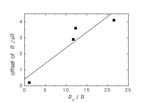
The offset values for two additional samples with (per-junction) resistances k and k (the samples for which the systematic -dependence was measured) were equal to 3.6 and 2.9, respectively. The corresponding theoretical predictions are 1.8 and 1.2. The data for the offsets are presented in Fig. 4. We observe that arrays with lower resistances show larger offsets, as predicted by our theory, Eq. (33). However, the offset values presented as a function of do not exactly fall on the straight line: they are scattered within an interval of . This effect could probably be attributed to the inhomogeneity of the arrays. For instance, the measured offsets for two arrays with nearly identical values of k and 2.2 k differ from each other. This discrepancy can be explained, if one assumes a certain degree of junction asymmetry, e.g., a 20 fluctuation of the per-junction resistance, , around the mean value, . This, in turn, can arise from a 40 % fluctuation in the area of the ”odd” and the ”even” tunnel junctions as a consequence of the two-angle evaporation technique employed in the sample fabrication.
The best linear fit for the offset – inverse resistance dependence (Fig. 4) yields , . The value agrees well with our theoretical prediction (34). At the same time the experimental value of turns out to be different from the predictions of the theory (35). It is also too uncertain due to the scattering of the data points. At present, possible reasons for this discrepancy remain unclear. We have checked asymmetry effects as well as those of the external environment within the framework of the Eq. (19). These effects can hardly help to improve the agreement between theoretical and experimental values of .
In the weak tunneling regime the offset is given by because . In order to check the effect of finite external resistance on the offset in this limit we have performed Monte-Carlo simulations (for details see [4, 19]) based on the phase-correlation theory [20]. The only fitting parameter used in these simulations was the junction capacitance. By comparing the measured conductance curves of the array represented by the solid triangles in Fig. 3 ( k) to those obtained from the numerical simulations, we have obtained the value fF for this sample. Notice that this value is in excellent agreement with that derived from Eq. (33) as explained above. We have also found that, depending on the magnitude of the environmental resistance, may increase by at most. Again this is not sufficient to explain the observed values of .
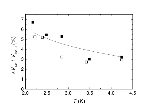
Figure 5 shows the variation of the normalized half-width as a function of temperature (. The solid and open squares represent the data measured for two 20-junction arrays both with k. The solid curve corresponds to our theoretical prediction, Eq. (23). We observe, that the difference between the experimental points and our theoretical curve typically does not exceed one percent, i.e. the ageement is fairly good.
Within the framework of our analysis, one can easily establish yet one more useful relation between the normalized half-width, , and the value of the conductance dip [cf, e.g., Eq. (19)] evaluated in the linear regime. Combining Eqs. (23) and (25) in the high temperature limit one gets
| (36) |
where the function in the strong tunneling limit reads
| (37) |
Note, that Eq. (36) was previously derived in Ref. [1] in the opposite weak tunneling limit , in which case the -function tends to the constant
| (38) |
We assume that in the intermediate regime the function is the sum of the expressions (37) and (38). This assumption, although not proven rigorously, provides a reasonable interpolation between the two limiting cases.
In addition to the arrays discussed above, three other samples with per-junction resistances of 20 k, 1.4 k, and 1.0 k were measured at K. The exact temperature was obtained from the vapor pressure of liquid helium. The corresponding data are collected into Table 1. The second row in the table represents the measured half-widths obtained directly from the measurement, . The corresponding conductance dips, , are shown in the third row. The forth row demonstrates the ”corrected” half-widths (i.e. the weak tunneling correction [Eqs. (36) and (38) subtracted],
| (39) |
In the weak tunneling regime this value would coincide with However in our experiments this is not the case. The fifth row shows the relative deviations of the corrected half-widths from that of the basic linear result, . In fact, the numbers in this row can be interpreted as the ”residual inaccuracies” of the measured half-widths as compared to the weak tunneling approximation. They can be explained by the strong tunneling effects. The corresponding theoretical values, obtained from the strong tunneling correction to the half-width of the conductance dip around zero bias voltage [Eq. (36, 37)], are shown in the last row of the table. These predictions are in a good agreement with the corrected measured data discussed above.
| (k) | 20 | 2.1 | 2.1 | 1.4 | 1.0 |
| (mV) | 40.20 | 41.90 | 41.32 | 42.22 | 41.91 |
| 2.15 | 2.32 | 2.26 | 2.21 | 1.79 | |
| (mV) | 39.85 | 41.52 | 40.96 | 41.86 | 41.62 |
| 0.5 | 4.7 | 3.3 | 5.6 | 5.0 | |
| 0.3 | 3.2 | 3.2 | 4.8 | 5.3 |
4 Conclusions
We have studied one-dimensional arrays of tunnel junctions in the strong tunneling regime, both theoretically and experimentally. Within the framework of the quasiclassical Langevin equation formalism, analytical expressions for the current-voltage characteristics of such arrays, together with the expressions for the half-width of the conductance dip around zero bias voltage, have been derived. Furthermore, the effect of external elecromagnetic environment has been studied theoretically. We have fabricated and measured several arrays of tunnel junctions with per-junction resistances ranging from 1 k to 23 k. Our measured data are in rather good agreement with the theoretical predictions. The experiments demonstrate that Coulomb blockade effects survive even in the strong tunneling regime, and are clearly visible in arrays with per-junction tunnel resistances as low as 1 k. These observations are in agreement with other recent experimental results on SET transistors [12] and on single junctions [13]-[15].
It has been verified, both in the theory and in the experiment, that high conductance arrays of tunnel junction are less favorable for Coulomb Blockade Thermometry (CBT) applications. This is a combined consequence of the more pronounced heating effects in such arrays, and the larger departure from the simple linear relation , which is of central role in the CBT applications. The latter, however, is not such a severe limitation, since corrections to the linear relation are now well known for all values of the junction resistance. It has also been shown that in the high temperature limit (in the leading approximation in ) the results for the conductance dip, now derived for arbitrary tunneling strength, coincide with those previously obtained in the weak tunneling regime.
References
- [1] J.P. Pekola, K.P. Hirvi, J.P. Kauppinen, and M.A. Paalanen, Phys. Rev. Lett. 73, 2903 (1994).
- [2] Sh. Farhangfar, K.P. Hirvi, J.P. Kauppinen, J.P. Pekola, J.J. Toppari, D.V. Averin, and A.N. Korotkov, J. Low. Temp. Phys. 108, 191 (1997).
- [3] J.P. Kauppinen, K.T. Loberg, A.J. Manninen, J.P. Pekola, and R.V. Voutilainen, Rev. Sci. Instrum. 69, 4166 (1998).
- [4] Sh. Farhangfar, A.J. Manninen, and J.P. Pekola, Europhys. Lett. 49, 237 (2000).
- [5] D.V. Averin and K.K. Likharev, in Mesoscopic Phenomena in Solids, ed. by B.L. Altshuler, P.A. Lee and R.A. Webb, Modern Problems in Condensed Matter Sciences 30 (North-Holland, Amsterdam, 1991).
- [6] J.P. Kauppinen and J.P. Pekola, Phys. Rev. B 54, R8353 (1996).
- [7] S.V. Panyukov and A.D. Zaikin, Phys. Rev. Lett. 67, 3168 (1991).
- [8] D.S. Golubev and A.D. Zaikin. Phys. Rev. B 46, 10903 (1992). A similar approach based on the analogy with the polaron problem was developed by A.A. Odintsov, Zh. Eksp. Teor. Fiz. 94, 312 (1988) [Sov. Phys. JETP, 67, 1265 (1988)].
- [9] D.S. Golubev and A.D. Zaikin. Phys. Lett. A169, 475 (1992).
- [10] D.S. Golubev and A.D. Zaikin. Zh. Eksp. Teor. Fiz. Pis’ma Red. 63, 953 (1996) [JETP Letters, 63, 1007 (1996)].
- [11] D.S. Golubev, J. König, H. Schoeller, G. Schön and A.D. Zaikin. Phys. Rev. B 56, 15782 (1997).
- [12] D. Chouvaev, L.S. Kuzmin, D.S. Golubev and A.D. Zaikin. Phys. Rev. B 59, 10599 (1999); Physica B (2000), to appear.
- [13] P. Joyez, D. Estève, and M.H. Devoret, Phys. Rev. Lett. 80, 1956 (1998).
- [14] Sh. Farhangfar, J.J. Toppari, Yu.A. Pashkin, A.J. Manninen, and J.P. Pekola, Europhys. Lett. 43, 59 (1997).
- [15] J.S. Penttila, U. Parts, P.J. Hakonen, M.A. Paalanen, and E.B. Sonin, cond-mat/9910298.
- [16] U. Eckern, G. Schön, and V. Ambegaokar, Phys. Rev. B 30, 6419 (1984).
- [17] G. Göppert and H. Grabert, cond-mat/9910237.
- [18] G. Göppert and H. Grabert, Phys. Rev. B 58, R10155 (1998).
- [19] K.P. Hirvi, M.A. Paalanen, and J.P. Pekola, J. Appl. Phys. 80 256 (1996).
- [20] G.-L. Ingold and Yu.V. Nazarov, in Single Charge Tunneling, ed. by H. Grabert and M.H, Devoret, NATO ASI Ser. B294 (Plenum, New York), Chapt. 2 (1992).