Intrinsic tunneling spectroscopy in small Bi2212 mesas
Vladimir Krasnov1,2, August Yurgens1,3, Dag Winkler4,1 and Per Delsing1
1 MINA, Chalmers University of Technology,
S41296, Göteborg, Sweden
2 Institute of Solid state
Physics, 142432 Chernogolovka, Russia
3 P.L.Kapitsa Institute, 117334 Moscow, Russia
4 IMEGO Institute, Aschebergsgatan 46, S41133, Göteborg, Sweden
Tunneling spectroscopy of high- superconductors (HTSC) provides an important information about quasiparticle density of states (DOS), which is crucial for understanding HTSC mechanism. Surface tunneling experiments [1, 2] showed, that besides the superconducting gap in the DOS, , there is a structure usually referred to as the ”pseudo-gap”, which exists well above . Both the behaviour of the superconducting gap and it’s correlation with the pseudo-gap are still a matter of controversy[1, 2].
To avoid drawbacks of surface tunneling experiments, such as dependence on the surface deterioration, surface states and undefined geometry[2], we used ”intrinsic” tunneling spectroscopy. HTSC single crystals can be considered as stacks of atomic scale intrinsic Josephson junctions (IJJ’s). Using microfabrication, it is possible to make small HTSC mesa structures with a well defined geometry[3]. Moreover, IJJ’s far from the sample surface can be measured, and deterioration of the sample surface becomes less important. Current-voltage characteristics (IVC’s) of mesas exhibiting tunnel junction behavior and can be used for studying DOS[4]. On the other hand, intrinsic tunneling spectroscopy can suffer from ohmic heating of the IJJ’s and steps (defects) on the surface of the crystal.
In this paper we present experimental data for small area Bi2Sr2CaCu2O8+x (Bi2212) mesas containing few IJJ’s. By decreasing the mesa area, , we minimize both the effect of overheating and the probability of defects in the mesa. Mesas with dimensions from 2 to 20 m were fabricated simultaneously on top of Bi2212 single crystals. First a long and narrow mesa was fabricated using photolithography and chemical etching. Next, insulating CaF2 layer was deposited and lift-off was used to make an opening. Finally, Ag film was deposited and electrodes were formed on top of the initial mesa by photolithography and Ar-ion etching. After etching, mesas beneath Ag electrodes remain.
In Fig.1, normalized IVC’s of three mesas at =4.2K and =150 K are shown. The vertical axis represents the current density, , and the horizontal axis shows the voltage per junction, . IVC’s for different samples are plotted by different colours. Parameters of the mesas are listed in Table 1. From Fig.1 it is seen, that the normalized IVC’s merge quite well into one curve. This indicates good reproducibility of the fabrication procedure. The -axis normal resistivity was, cm, where is the spacing periodicity of IJJ’s and is the resistance at large bias current and K.
| Table 1: | mesa | (m2) | ||
| S251b | 12 | 229.9 | ||
| S255b | 12 | 256.4 | ||
| S211b | 12 | 272.5 | ||
| S216b | 10 | 87 |
From Fig.1 it is seen that IVC’s exhibit clear tunnel junction behavior: (i) At low bias, multiple quasiparticle branches are seen, representing one-by-one switching of IJJ’s into the resistive state[3, 4]. The number of IJJ’s in the mesa was obtained by counting those branches. (ii) At intermediate currents there is a pronounced knee in IVC’s, representing the sum-gap voltage, . (iii) At high currents, there is a well defined normal resistance branch, . As seen from Fig.1, is almost temperature independent, as may be expected for a tunnel resistance. In contrast, the zero bias resistance, , increases sharply with decreasing , as shown in inset b).
Inset a) in Fig.1 shows temperature dependence of the gap voltage, , and the maximum spacing between multiple quasiparticle branches, , for four mesas on two diffrerent chips. Solid and open symbols represent branches for and , respectively. was determined at the ”maximum critical current”, at which the last IJJ switches to the resistive state, e.g. in Fig.1 that would correspond to A/cm2. This current is fluctuating from run to run, therefore, causing an uncertainty in determination of . From the inset a) it is seen, that is approximately two times less than . This is simply due to the fact that all the IJJ’s switch to the resistive state before they reach the gap voltage, see Fig.1. However, it is seen that the temperature dependence of reflects that for . The observed correspond to meV at =4.2 K, in agreement with [2].
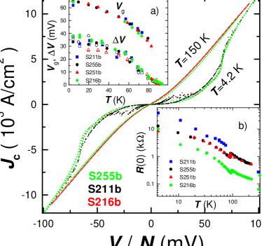
The IVC’s in Fig.1 suggest that there is no significant heating effect in our mesas. Indeed, overheating should cause the reduction of . Instead, we observed that the normalized IVC’s merge into a single curve with identical , despite a considerable difference in the dissipated power, . Moreover, we have checked that the voltages of the quasiparticle branches scale with their number, , where is the top branch, with all IJJ’s in the resistive state. Thus, switching of additional IJJ’s does not cause visible overheating of the mesa. On the other hand, we did observe a strong overheating for even smaller mesas (2 m2), containing larger number of IJJ’s , so that a clear back-banding was seen at large currents, and significantly lower was obtained, similar to that in Refs.[3, 5]. Therefore, a small number of IJJ’s in the mesa decreases the risk of overheating.
In Fig.2, the conductance at different temperatures is shown for one of the samples. The sharp peak at and the depletion of conductance at is seen at low , representing the superconducting gap in the DOS. The suppression of DOS below the gap results in strong temperature dependence of , see inset b) in Fig.1. With increasing temperature, the peak at shifts to lower voltages and decreases in magnitude. At 80 K, the peak is smeared out completely and only smooth depletion of the conductance remains at =0. With the further increase of , this depletion gradually decreases, but is still visible even at room temperature, representing the pseudo-gap in DOS. In agreement with the surface tunneling experiments[1, 2], there is almost no changes in the conductance at , which implies that the pseudo-gap coexists with the superconductivity.
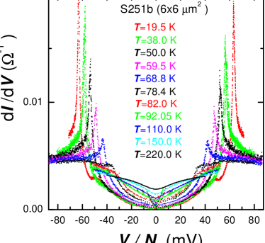
There is a crucial difference between our, ”intrinsic”, and the surface tunneling experiments[1, 2], which allows us to distinguish the superconducting gap from the pseudo gap. The difference is in existence of multiple quasiparticle branches in IVC’s, see Fig.1. Therefore, we have an additional quantity, the spacing between the quasiparticle branches, , which can be used for estimation of . Even though the peak in conductance is smeared out at 80 K, the quasiparticle branches in the IVC’s remain well defined up to . The continuously decreases with increasing and vanishes exactly at , as shown in inset a) in Fig.1.
This brings us to conclusion that the superconducting gap does close at , in contrast to the statement of Ref.[1]. On the other hand, the pseudo gap is almost independent of , in agreement with [1, 2]. The pseudo gap can exist well above and, probably, can coexist with the superconducting gap even at , see Fig.2. We can not conclude that the superconducting gap is developed from the pseudo gap nor that they are competing with each other. From our experiment, it seems more natural to assume that those two gaps are independent or only weakly dependent, despite having the same order of magnitude. In Ref. [6] possible scenarios of the pseudo gap were reviewed. One of the possible mechanisms is due to Coulomb charging effect in IJJ’s. Some experimental evidence for that was obtained in [5]. For the smallest mesas, we have also seen certain features, such as a complete suppression of the critical current and an offset voltage in IVC’s, which may be explained in terms of the Coulomb charging effect. However, further study is necessary before making a decisive conclusion about the origin of the pseudo-gap.
References
- [1] Ch.Renner, et al, Phys.Rev.Lett. 80(1998) 149
- [2] Y.DeWilde, et al, Phys.Rev.Lett. 80(1998) 153
- [3] A.Yurgens,et al, Physica C 235-240(1994)3269
- [4] M.Itoh, et al, Phys.Rev.B 55 (1997) R12001
- [5] Yu.I.Latyshev, et al, JETP Letters 69(1999) 84
- [6] J.Halbritter, Proc.SPIE 3480 (1998) 222