[
Double-dot charge transport in Si single electron/hole transistors
Abstract
We studied transport through ultra-small Si quantum dot transistors fabricated from silicon-on-insulator wafers. At high temperatures, 4 K 100 K, the devices show single-electron or single-hole transport through the lithographically defined dot. At K, current through the devices is characterized by multidot transport. From the analysis of the transport in samples with double-dot characteristics, we conclude that extra dots are formed inside the thermally grown gate oxide which surrounds the lithographically defined dot.
pacs:
PACS numbers: 73.23.Hk, 85.30.Wx, 85.30.Vw, 85.30.Tv
]
Recent advances in miniaturization of Si metal-oxide-semiconductor field-effect transistors (MOSFETs) brought to light several issues related to the electrical transport in Si nanostructures. At low temperatures and low source-drain bias Si nanostructures do not follow regular MOSFET transconductance characteristics but show rather complex behavior, suggesting transport through multiply-connected dots. Even in devices with no intentionally defined dots (like Si quantum wires[2, 3, 4, 5] or point contacts[6]) Coulomb blockade oscillations were reported. In the case of quantum wires, formation of tunneling barriers is usually attributed to fluctuations of the thickness of the wire or of the gate oxide. However, formation of a dot in point contact samples is not quite consistent with such explanation. Recently in an elegant experiment with both and source/drain connected to the same Si point contact Ishikuro and Hiramoto[7] have shown that the confining potential in unintentionally created dots is similar for both holes and electrons. However, there is no clear picture where and how these dots are formed.
In this work we analyze the low temperature transport through an ultra-small lithographically defined Si quantum dots. While at high temperature 4 K 100 K we observe single-electron tunneling through the lithographically defined dot, at K transport is found to be typical for a multi-dot system. We restrict ourselves to the analysis of samples with double-dot transport characteristics. From the data we extract electrostatic characteristics of both the lithographically defined and the extra dots. Remarkably, transport in some samples cannot be described by tunneling through two dots connected in sequence but rather reflects tunneling through dots connected in parallel to both source and drain. Taking into account the geometry of the samples we conclude that extra dots should be formed within the gate oxide. Transport in p- and n-type samples are similar, suggesting that the origin of the confining potential for electrons and holes in these extra dots is the same.
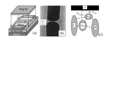
The samples are metal-oxide-semiconductor field-effect transistors (MOSFETs) fabricated from a silicon-on-insulator (SOI) wafer. The top silicon layer is patterned by an electron-beam lithography to form a small dot connected to wide source and drain regions, see schematic in Fig. 1a. Next, the buried oxide is etched beneath the dot transforming it into a free-standing bridge. Subsequently, 40 or 50 nm of oxide is thermally grown which further reduces the size of the dot. Poly-silicon gate is deposited over the bridge with the dot as well as over the adjacent regions of the source and drain. It is important to note that in this type of devices the gate not only controls the potential of the dot but also changes the dot-source and dot-drain barriers. Finally, the uncovered regions of the source and drain are n–type or p–type doped. More details on samples preparation can be found in Ref. [8]. Totally, about 30 hole and electron samples have been studied. Here we present data from two samples with hole (H5A) and electron (E5-7) field-induced channels.
An SEM investigation of test samples, Fig. 1b, reveals that the lithographically defined dot in the Si bridge is 10-40 nm in diameter and the distance between narrow regions of the bridge is 70 nm. Taking into account the oxide thickness we estimate the gate capacitance to be 0.8–1.5 aF.
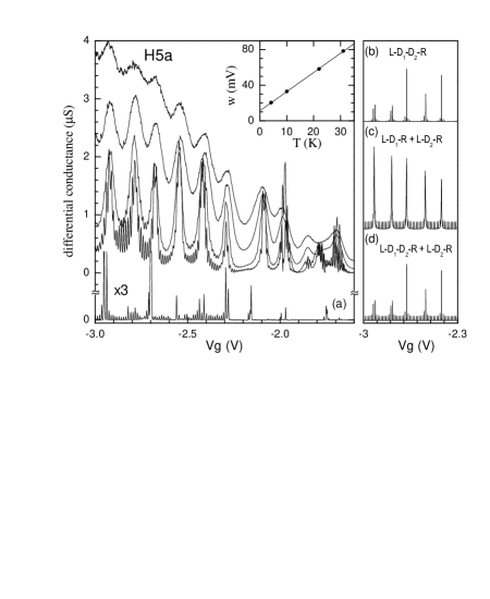
In most of our samples (with both n– and p–channel) we see clear Coulomb blockade oscillations with a period mV up to 100 K. A typical charge addition spectra is plotted in Fig. 2 and Fig 3 for samples H5A and E5-7. In H5A the spectrum is almost periodic as a function of the gate voltage at K with the period mV. Assuming that each peak corresponds to an addition of one hole into the dot we calculate the gate capacitance aF, which is within the error bars for the capacitance estimated from the sample geometry. The lineshape of an individual peak can be described[9, 10] by , where is the peak position and coefficient relates the change in the to the shift of the energy levels in the dot relative to the Fermi energy in the contacts. This expression is valid if both coupling to the leads and single-particle level spacing are small: . We fit the data for H5A with in the range -3.0 V V and the extracted is plotted in the inset in Fig. 2. From the linear fit [mV] we find the coefficient [mV/meV], thus the Coulomb energy is meV and the total capacitance aF. The main contribution to comes from dot-to-lead capacitances (an estimated self-capacitance is a few aF). The extrapolated value of at zero temperature provides an estimate for the level broadening meV.
At K oscillations with another period, much smaller than , appear as a function of . The small period is in the range mV in different devices ( mV for the sample in Fig. 2). This small period is due to a single-hole tunneling through a second dot and the corresponding gate capacitance aF. However, there is no intentionally defined second dot in our devices. Below we first analyze the experimental results and then discuss where the second dot can be formed.
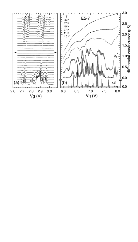
At low temperatures and small gate voltages (close to the turn-on of the device at high temperatures) current is either totally suppressed, as in E5-7 at V, Fig. 3a, or there are sharp peaks with no apparent periodicity, as in H5A at V, Fig. 2. Both suppression of the current and “stochastic Coulomb blockade”[11] are typical signatures of tunneling through two sequentially connected dots. The non-zero conductance can be restored either by raising the temperature (Fig. 2) or by increasing the source-drain bias (Fig. 3a). In both cases, is modulated with and , consistent with sequential tunneling. We conclude that in these regime the two dots are connected in series L-D1-D2-R (see schematic in Fig. 1c).
At larger gate voltages ( V for E5-7 and V for H5A) current is not suppressed even at the lowest temperatures. However, the pattern is different in the H5A and E5-7 samples. In H5A, the oscillations with have approximately the same amplitude (except for the sharp peaks which are separated by approximately ), while in E5-7 the amplitude of the fast oscillations is modulated by . Also, the dependence of the amplitude of the fast modulations on the average conductance is different: in H5A the amplitude is almost -independent, while in E5-7 it is larger for larger .
Non-vanishing periodic conductance at low temperatures requires that the transport is governed by the Coulomb blockade through only one dot D2. That can be achieved either if both barriers between the contacts and the D2 become transparent enough to allow substantial tunneling or if the strong coupling between the main dot D1 and one of the leads results in a non-vanishing density of states in the dot at . If we neglect coupling between the dots, in the former case the total conductance is approximately the sum of two conductances, , where is conductance through the main dot L-D1-R and is conductance through the second dot L-D2-R. This case is modeled in Fig 2c using experimentally determined parameters of sample H5A. From the analysis of high-temperature transport we found that the zero-temperature broadening of D1 peaks mV mV and that should be exponentially suppressed between D1 peaks at K if the dots are connected in series L-D1-D2-R, Fig 2b. The best description of the low temperature transport at -3.0 V V in H5A is achieved if we assume that there are two conducting paths in parallel: through the extra dot L-D2-R and through both dots together L-D1-D2-R, Fig 2d.
In the latter case, the dots are connected in series L-D1-D2-R. At high the barrier between L and D1 is reduced giving rise to a large level broadening . The total conductance is , where is the Coulomb blockade conductance through D2 alone and is the Breit-Wigner conductance through D1 and . In this case is following and is modulated by . Moreover, if we assume that the amplitude of is not a strong function of , the amplitude of modulation will be a function of , namely the larger the larger the amplitude of the modulation of the total conductance. This model of two dots in series with one being strongly coupled to the leads is in qualitative agreement with the data from sample E5-7.
Non-equilibrium transport through E5-7 is shown in Fig. 4 with a single vs. trace at a fixed shown at the top of the figure. White diamond-shaped Coulomb blockade regions are clearly seen on the gray-scale plot. Peaks in at positive bias are due to asymmetry in the tunneling barriers[12]: at negative biases tunneling to the dot is slower than tunneling off the dot and only one extra electron occupies the dot at any given time, thus only one peak, corresponding to the onset of the current, is observed (we have not seen any features due to the size quantization, which is not surprising if we take into account the large number of electrons in this dot). At positive biases current is limited by the time the electron spends in the dot before it tunnels out. In this regime an extra step in the I-V characteristic (and a corresponding peak in its derivative ) is observed every time one more electron can tunnel into the dot. These peaks, marked with arrows, are separated by the charging energy meV.
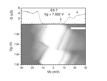
Electrostatic parameters of the D2 dot can be readily extracted from Fig. 4. The source, drain and gate capacitances are 8.5, 2.7 and 6.4 aF and the corresponding charging energy is meV. The charging energy of meV is obtained by analyzing Fermi-Dirac broadening of the conductance peaks as a function of temperature and the period of oscillations. The fact that it requires the application of mV to lift the Coulomb blockade means that in the Coulomb blockade regime all the bias is applied across the second dot, consistent with large conductance through D1.
Where does the second dot reside? One possibility is that the silicon bridge, containing the lithographically defined dot, breaks up at low temperatures as a result of the depletion due to variations of the bridge thickness and fluctuations in the thickness of the gate oxide, or due to the field induced by ionized impurities. However, in this case should be less than . In fact, if we assume that the thickness of the thermally grown oxide is uniform, the gate capacitance of the largest possible dot in the channel cannot be larger than 1.5 aF. Also, if at low temperatures the main dot would split into two or more dots we should see the change in the period of the large oscillations[13], inconsistent with our observations.
Another possibility is that the dot is formed in the contact region adjacent to the bridge. Given that the oxide thickness is 40 nm, the second dot diameter should be nm. We measured two devices which have 30 nm wide and 500 nm long channels, fabricated using the same technique as the dot devices. Both samples show regular MOSFET characteristics down to 50 mK. Thus, it is unlikely that a dot is formed in the wide contact regions of the device. Even if such a dot was formed occasionally in some device by, for example, randomly distributed impurities, it is unlikely that dots of approximately the same size would be formed in all samples. Another argument against such a scenario is that if the second dot is formed inside one of the contact regions, it cannot be coupled to the other contact to provide a parallel conduction channel, as in sample H5A.
Thus, the second dot should reside within the gate oxide, which surrounds the lithographically defined dot. Some traps can create confining potential in both conduction and valence bands, for example Pb center has energy levels at eV and eV. Several samples show a hysteresis during large gate voltage scans accompanied by sudden switching. This behavior can be attributed to the charging-discharging of traps in the oxide. If such a trap happens to be in a tunneling distance from both the lithographically defined dot and a contact, or the trap is extended from one contact to the other, it may appear as a second dot in the conductance.
To summarize our results, we performed an extensive study of a large number of Si quantum dots. We found that all devices show multi-dot transport characteristics at low temperatures. From the data analysis we arrived at the conclusion that at least double-dot behavior is caused not by the depletion of the silicon channel but by additional transport through traps within the oxide.
We acknowledge the support from ARO, ONR and DARPA.
REFERENCES
- [1] Current address: Department of Electrical Engineering and Computer Science, University of Michigan, Ann Arbor, MI 48109.
- [2] Y. Nakajima, Y. Takahashi, S. Horiguchi, K. Iwadate, H. Namatsu, K. Kurihara, and M. Tabe, Jpn. J. Appl. Phys. 34, 1309 (1995).
- [3] H. Ishikuro, T. Fujii, T. Saraya, G. Hashiguchi, T. Hiramoto, and T. Ikoma, Appl. Phys. Lett. 68, 3585 (1996).
- [4] T. Hiramoto, H. Ishikuro, T. Fujii, G. Hashiguchi, and T. Ikoma, Jpn. J. Appl. Phys. 36, 4139 (1997).
- [5] R. A. Smith Abd H. Ahmed, Appl. Phys. Lett. 71, 3838 (1997).
- [6] H. Ishikuro and T. Hiramoto, Appl. Phys. Lett. 71, 3691 (1997).
- [7] H. Ishikuro and T. Hiramoto, Appl. Phys. Lett. 74, 1126 (1999).
- [8] E. Leobandung, L. Guo, Y. Wang, and S. Y. Chou, Appl. Phys. Lett. 67, 938 (1995).
- [9] I. O. Kulik and R. I. Shekhter, Zh. Eksp. Teor. Fiz. 68, 623 (1975), [Sov. Phys. JETP 41, 308 (1975)].
- [10] C. W. J. Beenakker, Phys. Rev. B44, 1646 (1991).
- [11] I. M. Ruzin, V. Chandrasekhar, E. I. Levin, and L. I. Glazman, Phys. Rev. B45, 13469 (1992).
- [12] B. Su, V. J. Goldman, and J. E. Cunningham, Phys. Rev. B46, 7644 (1992).
- [13] F. R. Waugh, M. J. Mar, R. M. Westervelt, K. L. Campman, and A. C. Gossard, Phys. Rev. Lett.75, 705 (1995).