-Axis tunneling in YBa2Cu3O7-δ/PrBa2Cu3O7-δ superlattices
Abstract
In this work we report -axis conductance measurements done on a superlattice based on a stack of 2 layers YBa2Cu3O7-δ and 7 layers PrBa2Cu3O7-δ (2:7). We find that these quasi-2D structures show no clear superconducting coupling along the -axis. Instead, we observe tunneling with a gap of meV for the direction perpendicular to the superconducting planes. The conductance spectrum show well defined quasi-periodic structures which are attributed to the superlattice structure. From this data we deduce a low temperature -axis coherence length of nm.
pacs:
74.80.Dm,73.61.-r,73.20.DxAs for classical superconductors, tunneling experiments are a direct way of testing the local superconducting density of states [1]. In particular the co-existence of - wave and -wave components of the order parameter was directly investigated from -axis planar tunneling measurements done in high temperature superconductors (HTS) [2, 3]. However tunneling experiments are extremely sensitive to the quality of barriers and interfaces. This aspect explains the extreme care taken by the different groups in the fabrication of HTS tunnel junctions. One way of getting around this problem is to investigate -axis tunneling in YBa2Cu3O7-δ/PrBa2Cu3O7-δ superlattices (Y123/Pr123). In those systems it is possible to modify the tunneling properties simply by varying the periodicities of the Y123 and Pr123 layers. Another advantage is that transmission electron microscope (TEM) studies show atomically flat Y123/Pr123 interfaces in superlattices [4].
In this work we study the influence of the periodicity of an artificial superlattice on the local superconducting density of states of Y123. This was only possible by a sustained effort divided in three main steps: the preparation of high quality Y123/Pr123 superlattices, the patterning of suitable mesa structures and the measurement of the -axis transport properties.
Y123/Pr123 superlattices are deposited on a similar way as Y123 thin films. The only difference is that after sputtering one to 10 unit cells (u.c.) of Y123 the substrate is turned to a cathode containing the Pr123 target. This process is repeated until a total film thickness of 200 nm. The switching between targets is made with a computer-controlled step motor. To provide low ohmic contacts the process ends by the in-situ deposition of a protective gold layer with thickness from 200 to 400 nm. In order to avoid the formation of pin-holes and reduce the surface roughness the sputtering process was done at 3 mbar pressure of a mixture 1 to 2 of O2 and Ar.
The crystallographic quality of the superlattices used in this work has been checked by x-ray diffraction. Our measurements showed up to third order satellite peaks observed in () scans. On the other hand TEM studies show steps of only 1 u.c. for every 100 nm. This value is much smaller than the 7 u.c. thick Pr123 barrier.
Given that a Gold layer covered the superlattices the surface morphology could not be checked directly on the same samples where the -axis measurements were done. However scanning tunneling microscopy done in similar superlattices reveal an average surface modulation of 7.2 nm (6 u.c.) for a length scale of 1.6 m. This roughness is very small when compared to the total thickness of the mesas which was of about 120 nm. Since the measurements below were performed on 2:7 superlattices and the top layer was always Y123, only the two upper Y123 layers (of a total of 10) are probably affected by the protective gold layer. This is expected to have little influence on our experimental results.
Before making the mesa structures, a ground electrode with 1.2 10 mm2 was wet chemically etched. The mesas were later on prepared by standard UV-photolithography and ion milling. During the etching process the samples were cooled down to 77 K. Later the chip was coated with photoresist, and a window was opened on the top of each mesa by a photolithographic process. The preparation step ends with the deposition of a gold top electrode patterned by wet chemical etching. Because of its smoothness, high homogeneity and low defect density the photoresist was directly used for insulating the top contact from the ground electrode. All measurements were done in a ”three point” geometry, where the typical contact resistance between the HTS material and gold is cm2. For the moment, we are limited to mesa structures down to 1515 m2.
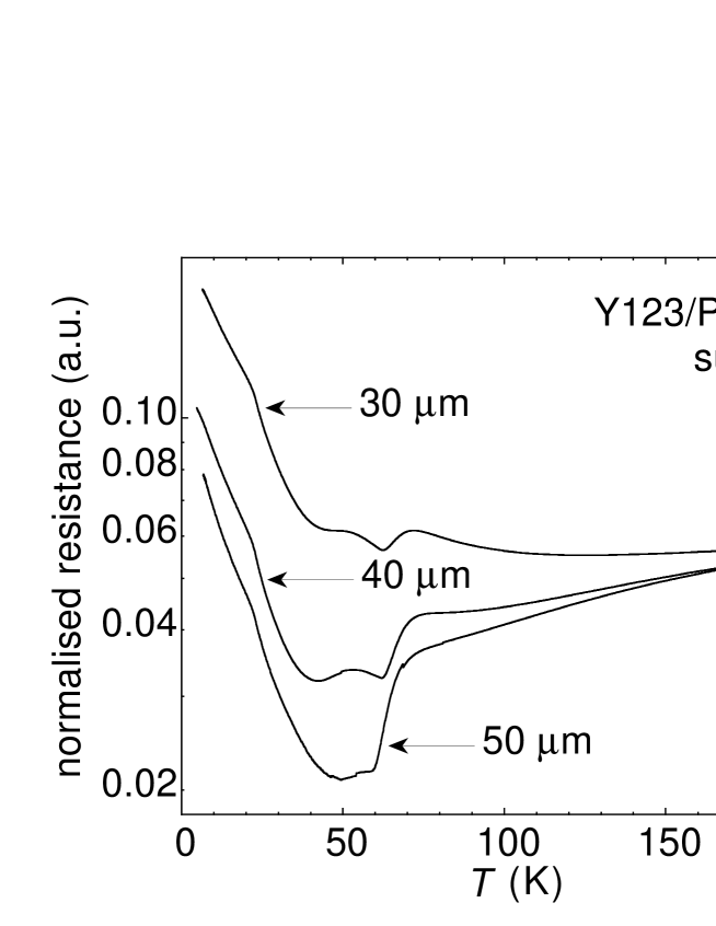
In Fig. 1 we show a semi-logarithmic plot of the resistances of three mesas with , and m2 prepared on a Y123/Pr123 superlattice with 2 layers Y123 and 7 layers Pr123 (2:7). The transition observed at 65 K corresponds to the superconducting transition of the Y123 layers. The reduced is typical for the non-fully developed order parameter in the 2 u.c. thick Y123 layer [5]. Above , the larger mesas show a temperature dependence that is similar to the one measured in the (a,b)-plane. This demonstrates that we measured a non-negligible amount of the (a,b) component. However below the superconducting Y123 layers define equipotential planes, and only the -axis component of the resistance can be measured. This is confirmed by the vertical shift existing between the different plots shown in Fig. 1. The logarithmic y- axis shows that the different curves differ below only by a proportionality factor. The resistances of the mesas at 20 K were , and which give ratios of (expected ) and (). The discrepancy of 30% observed in the can be attributed to a larger degree of damage introduced during the etching of the m mesa. The contact resistance of the gold top electrode should scale as well with the area of the mesas.
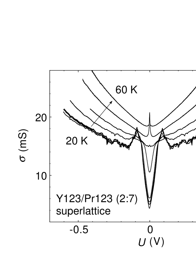
We measured simultaneously the vs. characteristics and the differential resistance in the m2 mesa. This was done by using a battery operated current source that superposes above an arbitrary DC current, a small AC signal generated by the reference of a Lock-in amplifier. The DC-and AC-signals were measured with an HP34420A nano-voltmeter and a PAR 5210 Lock-in amplifier respectively. In Fig. 2 we show some of our results on a m2 mesa done on a 2:7 superlattice for temperatures between 2.0 and 60 K. Several features can be identified in Fig. 2. The first is the parabolic background which can be well described by the Simmons model which predicts [6]:
| (1) |
This model corresponds to a metal-insulator-metal junction with a rectangular barrier of width and height . The constant factors are and where . Considering that we have 10 bi-layers connected in series, we deduced from Eq. 1 that each Pr123 barrier has below K an effective height meV and an effective width nm. Although is much smaller than the 8.2 nm expected from the u.c., we can explain this result by pure geometrical arguments. If we take into account the imperfections in the superlattice (steps of 1 u.c. per interface) and the fact that superconductivity extends to the chains (0.5 u.c. per interface), we would have an effective barrier thickness of nm (4 u.c.). This crude estimation is only larger than . From our data we deduce that the values of and were practically temperature independent up to K. Above this temperature the conductivity follows the behavior characteristic for resonant tunneling via up to two localized states [7]:
| (2) |
The two peaks observed at lower temperatures in should indeed correspond to a -axis superconducting gap. The distance between the two peaks is mV. This particular mesa was made with a height of about 120 nm estimated from an etching rate calibrated by Atomic Force Microscopy done in different etched films. This gives a stack of to bi-layers which present each a -axis superconducting gap of meV.
This value is in excellent agreement with the value of given in the literature which scatters between 4 and 6 meV for planar junctions prepared with Pr123, CeO2 and SrAlTaO6 barriers [8, 9, 10, 11]. To understand this result we have to look at Scanning Tunneling Spectroscopy (STS) data. Typical STS measurements done on both Y123 thin films and high quality single crystals give gap structures at about 5 and 20 meV [12, 13].These fine structures observed in tunneling spectra were explained successfully by Miller at al by considering that Y123 is constituted by a stack of strong and weak superconducting layers which contribute with different weights to the tunneling spectra [12, 14]. In particular the 5 meV gap has been attributed to the BaO and CuO layers situated between the CuO2 blocks. Since these BaO and CuO layers are common to both Y123 and Pr123 we expect them to constitute the interfaces which are relevant to our tunneling process. Given that in our superlattices is only reduced by 20% we do not expect the CuO2 superconducting gap to be strongly suppressed. On the other hand given that a 4-6 meV gap structures are observed in measurements done with different barriers we think that the gap meV is indeed an intrinsic property of Y123. The existence of this small c-axis gap is consistent with the strong thermal smearing of the gap feature at about 50 K, which corresponds to an energy of the same magnitude as .
For the moment it is not clear to us which will be the influence of the CuO chains to the symmetry of the order parameter. However since these chains form together with the apical oxygen CuO2 cells oriented along to the - axis, it is likely that a -axis gap would exist in Y123 with a -wave like symmetry.
To enhance the other features present in , we plot in Fig. 3 for temperatures between 2.0 and 65 K. For more clarity the data is vertically shifted. Below 25 K the Simmons model is used to calculate (Eq. 1). Above that temperature the resonant tunneling expression given by Eq. 2 is employed. We would like to emphasize that for all temperatures the low bias features were included in the estimation of .
Below 30 K we observe a number of reproducible features which were superposed to the superconducting gap. For increasing temperatures, the gap and these structures are smeared out by thermal fluctuations. At about 30 K the only signature of the gap is a soft voltage dependence of and a zero bias peak which starts to develop, grows up to about 50 K and finally disappears near .
Although there is not for the moment a clear explanation for the origin of this zero bias peak, its disappearance close to shows that it is clearly related to tunneling of superconducting pairs. As suggested by Abrikosov [15] this anomaly could be due to resonant tunneling through localized states in the barrier. The absence of a zero bias peak at lower temperatures is consistent with this picture: the success in fitting the data with a Simmons model indicates that below 25 K, the Pr123 layers behave predominantly like normal tunneling barriers having one or no resonant states.
The arrows in Fig. 3 show sharper indentations in which can be followed up to 30 K. To investigate the additional features present in the low temperature conductivity we plot in Fig. 4 for U between 0.1 and 0.5 V. The vertical lines correspond to the minima of the oscillations which are particularly visible at lower temperatures. To find the periodicity of these oscillations, we plot in Fig. 5 vs. an integer index . A clear zero crossing of the linear fit is obtained by choosing an index n=9 for the lowest extracted value of . From the linear fit we deduce a period of mV. If we remember that this value corresponds to 8-10 junctions connected in series, a single junction would show a periodicity of meV.
The expected -axis density of states of a superlattice where the superconducting gap is a one dimensional periodic step has been already calculated by van Gelder in 1969 [16]. With the HTS materials, the increasing interest on superlattices inspired the work of Hahn in extending the model to the three dimensional case [17]. These models predict the opening of gaps which were particularly visible in the one dimensional case. In the 3-dimensional case they are smeared out, although still present. The main result from Ref. [17] is that above the superconducting gap these additional gap structures should appear with a periodicity of:
| (3) |
where is the periodicity of the superlattice, the -axis coherence length, the -axis gap and the periodicity of the sub-gap structures. By taking nm, and meV we deduce from Eq. 3 a -axis coherence length of nm [18]. This result is close to the value of nm deduced from an analysis of fluctuation conductivity in Y123/Pr123 superlattices [19]. If we assume for Y123 an anisotropy of [20] we would obtain a in-plane coherence length nm. This value is close to the generally quoted nm for Y123 [21]. The larger structures indicated by the arrows in Fig. 3, correspond to a periodicity of mV. It is interesting to notice that the ratio of this periodicity divided by the periodicity of is .This value corresponds to the ratio between and a Y123 unit cell! From Eq. 3 and Fig. 4 we deduce that is practically temperature independent below 20 K.
We show in this paper that by constructing superlattices it is possible to generate sub- gap structures. These features can be directly used to determine in an independent way a - axis coherence length nm for a 2 u.c. thick Y123.
The agreement of these results with previous estimations of Y123 coherence lengths shows that meV could be indeed a -axis superconducting gap related to the CuO chains.
From the observed sub-gap structures, we conclude that is practically temperature independence below 20 K.
Due to thermal fluctuations, this analysis could not be extended up to higher temperatures.
The authors would like to thank K. Gray, J.F. Zasadzinski, R.A. Klemm, R. Schilling and J. Mannhart for valuable and stimulating discussions. This work was supported by the German BMBF through Contract 13N6916 and the European Union through the Training and Mobility of Researchers (ERBFMBICT972217).
REFERENCES
- [1] Ivar Giaever, Phys.Rev.Lett. 5 147 (1960)
- [2] A.G. Sun, D.A. Gajewski, M.B. Maple, R.C. Dynes, Phys.Rev.Lett. 72 2267 (1994)
- [3] R.Kleiner et al. Phys.Rev.Lett.72 593 (1994)
- [4] C.L.Jia, H.Soltner, G.Jakob, Th.Hahn, H.Adrian, and K.Urban, Physica C 210 1 (1993)
- [5] G. Jakob, T. Hahn, C. Stölzel, C.Tomé-Rosa, H. Adrian, Europhys.Lett. 19 135 (1992)
- [6] J.G. Simmons, J. Appl. Phys. 34 238 (1963)
- [7] L.I. Glazman, K.A. Matveev, Sov.Phys. JETP 67 1276 (1988)
- [8] I. Iguchi, Z. Wen, Physica C 178 1 (1991)
- [9] Q.Y. Ying, C. Hilbert, Appl.Phys.Lett. 65 3005 (1994)
- [10] M.A. Bari, F.Baudenbacher, J. Santiso, E. J. Tarte, J.E. Evets, M.G.Balmire, Physica C, 256 227 (1996)
- [11] K. Nakajima, T. Arai, S.E. Shafranjuk, T. Yamashita, I. Tanaka, H. Kojima, Physica C, 293 292 (1997)
- [12] T.G. Miller, M. McElfresh, R. Reifenberger, Phys.Rev.B 48 7499 (1993)
- [13] I. Maggio-Aprile, Ch. Renner, A. Erb, E. Walker, ØFischer, Phys.Rev.Lett. 75 2754 (1995)
- [14] M. Tachiki, S. Takahashi, F. Stegkich, H. Adrian, Z. Phys B 80 161 (1990)
- [15] A.A.Abrikosov, Phys.Rev.B 57 7488 (1998)
- [16] A.P. van Gelder, Phys.Rev. 181 787 (1969)
- [17] A. Hahn, Physica B, 165-166 1065 (1990)
- [18] Since is here deduced from the ratio , our results are independent from the number of junctions constituting the stack.
- [19] A.L. Solovjov , V.M. Dmitriev, H.-U. Habermeier, I.E. Trofimov, Phys.Rev.B 55 8551 (1997)
- [20] B. Janossi D. Prost, S. Pekker, L. Fruchter, Physica C 181 51 (1991)
- [21] Michael Tinkham, Introduction to Superconductivity, 2nd ed. 325 (1996)