The optical performance of frequency selective bolometers
T.A. Perera, T.P. Downes, S.S. Meyer, and T.M. Crawford
University of Chicago, KICP, Chicago, IL 60637, U.S.A
E.S. Cheng
Conceptual Analytics, Glenn Dale, MD 20769, U.S.A.
T.C. Chen, D.A. Cottingham, and E.H. Sharp
Global Science and Technology, Greenbelt, MD 20771, U.S.A.
R.F. Silverberg
NASA/GSFC, LASP, Greenbelt, MD 20771
F.M. Finkbeiner and D.J. Fixsen
SSAI, Greenbelt, MD 20706
D.W. Logan and G.W. Wilson
University of Massachusetts, Department of Astronomy, Amherst, MA 01003, U.S.A.
Frequency Selective Bolometers (FSBs) are a new type of detector for millimeter and sub-millimeter wavelengths that are transparent to all but a narrow range of frequencies as set by characteristics of the absorber itself. Therefore, stacks of FSBs tuned to different frequencies provide a low-loss compact method for utilizing a large fraction of the light collected by a telescope. Tests of prototype FSBs, described here, indicate that the absorption spectra are well predicted by models, that peak absolute absorption efficiencies of order 50% are attainable, and that their out-of-band transmission is high.
1 Introduction
The millimeter and sub-millimeter wavelengths are a proven spectral range for tracing the evolutionary history of our universe. With sources ranging from the cosmic microwave background, to high-redshift starburst galaxies, to galaxy clusters, to cold dusty objects in our own galaxy, this portion of the spectrum is uniquely fertile with information on cosmological parameters, growth of structure from the linear through the non-linear regime, star formation history and galactic dynamics. Advances in detector technology at millimeter and sub-millimeter wavelengths have resulted in receiver sensitivities approaching the background limit. More recently, large format arrays have been developed at these wavelengths for imaging from single-dish telescopes (e. g. BOLOCAM, AzTEC, SHARC-2, SCUBA-2) and a new era of high angular resolution ground-based observing will soon begin with the first-light of the 50 m Large Millimeter Telescope (LMT) and the Atacama Large Millimeter Array (ALMA) array.
Increasing detector count and field of view is not the only avenue for improvement of today’s photometers. Typically there is a large mismatch between the working bandwidth of telescopes and the bandwidth of focal plane arrays. We describe the concept and first characterization of a new form of bolometric detector designed to alleviate this inefficiency at millimeter and sub-millimeter wavelengths. Frequency Selective Bolometers (FSBs) facilitate a dramatic improvement in the fraction of radiation utilized by a compact and convenient focal plane array.
Multi-frequency photometric capabilities are currently achieved with identical detectors behind dichroic beam-splitter setups or behind different filters on an allocated focal plane. These complex arrangements make inefficient use of valuable focal plane area and/or reduce optical efficiency with multiple chromatic splitters and numerous reflections. In addition, the focal plane optics can be physically large, massive, and difficult to cool down to sub-Kelvin temperatures and integrate into the tight constraints imposed on orbital and sub-orbital missions. FSB technology removes many of these problems by incorporating a bolometer element into a resonant structure to control the range of absorbing frequencies. The key advantage of the FSB is that radiation not absorbed by the bolometer is transmitted with low loss through the device and passed on to subsequent FSB elements tuned to other frequencies.[1] A stack of FSBs, is therefore, a multi-spectral single pixel with an angular resolution set by the lowest frequency detector. Adjacent stacks of FSBs can be efficiently close-packed into an array of multi-color pixels populating the focal plane.
The SPEctral Energy Distribution (SPEED) camera,[2, 3] scheduled for commissioning in spring 2007, will be the first instrument to make use of FSB technology. SPEED will have four focal plane pixels, each sensitive to four separate frequency bands centered around 148, 219, 271, and 361 GHz. It will be used for photometry of distant dusty galaxies previously found by surveys like Spitzer and SCUBA, and for studying other millimeter-wave sources such as ultra luminous infrared galaxies, the Sunyaev-Zeldovich effect in clusters, and galactic dust. We present here the design and characterization of SPEED prototype detectors.
2 Optical design
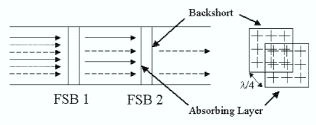
FSBs incorporate frequency selective surfaces as part of the detector to define the absorption band. High out-of-band transmission allows multiple, differently tuned FSBs to be stacked in series to create a compact multi-color photometer. Fig. 1 outlines the concept of FSBs in a two color photometer.
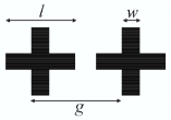
The optical performance of an individual FSB is characterized by the spectral profile of its absorption, the absolute efficiency of the absorption, and its transparency to radiation outside the absorption band. The crossed-dipole geometry (see Fig. 2) of the FSBs described in this paper has been shown to produce a narrow resonance with out-of-band transmission near unity.[4] The absorber and backshort geometries are described by three parameters: the bar length, , the bar width, , and the periodicity of the grid, . The resonant wavelength is near and has a weak dependence on .[5]
Unlike frequency selective surfaces used strictly as reflective filters, FSBs require efficient absorption of incident radiation. The frequency selective absorbers are made lossy to match the impedance of free space and maximize coupling to plane wave radiation. Previous studies of lossy frequency selective elements have demonstrated how resistive periodic elements can efficiently absorb radiation within narrow bands [6]. The absorption of an FSB is enhanced when paired with a similarly resonant but purely reflective (lossless) backshort located one quarter wavelength behind the absorber. The backshort separation and other parameters that maximize absorption at the chosen frequency fully constrain the spectral profile of the absorption. While both components of polarization are absorbed by the FSBs discussed here, polarization sensitivity may be achieved by replacing crosses in the metallic patterns with bars.
2.A HFSS modeling
We numerically calculate the spectral response of potential FSB designs to optimize the spectral shape and absorption efficiency. We use Ansoft’s High Frequency Structure Simulator (HFSS)[7] to predict the transmission, reflection, and absorption of each detector. While isolated crossed dipole frequency selective surfaces have been described analytically with some success,[8] HFSS allows modeling of realistic devices with substrate materials and interactions between adjacent resonant meshes.
Each FSB is modeled as a unit cell with side lengths equal to the periodicity of the grid and periodic boundary conditions on four sides to simulate an infinite pattern of crosses. Two perfectly matched layers (PMLs)[9, 10] on the top and bottom of the unit cell terminate the incident wave and minimize edge effects. Inside the unit cell are two aligned 2-D crosses representing an absorbing and a backshort layer on substrates separated by a distance of and normal to the plane wave excitation. The spectral performance of the FSB is calculated by solving for the transmission () and reflection () of incident plane waves at frequencies where the unit cell model is valid (). Absorption is estimated as . These models are used to optimize the spectral profile of all FSB designs before fabrication.
2.B Physical description
We have fabricated a set of FSBs with target resonant frequencies of 219 and 271 GHz. The devices were fabricated at the NASA Goddard Space Flight Center (GSFC) using photolithographic techniques.
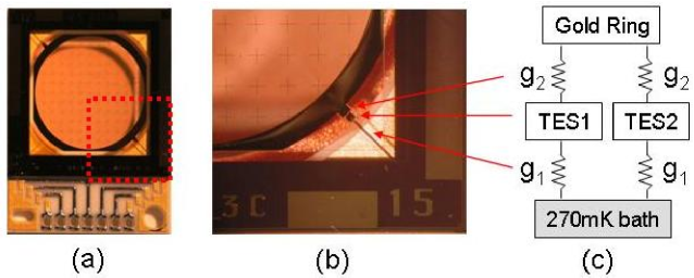
The absorber and backshort layers are built on a 0.5 m thick film of Si3N4 which is suspended from a Si frame. The size of the suspended windows is approximately mm. The backshort cross pattern is formed of Au 200 nm thick to provide high conductivity. The absorbing layer has Au 28 nm thick corresponding to a sheet resistance of 1.6 /square, the value determined by simulations to optimize absorption. Because currents are highest near the edges of patterned features, a lift-off process with an overhang on the resist is used to obtain sharp edges. The crosses are arranged to fill a 10 mm diameter light pipe centered on the element. Table 1 gives the geometric properties of the crossed dipole surfaces of each FSB.
To form an FSB, the bolometer and backshort are glued together with a Si shim of thickness . The crosses on the two layers must be registered to better than for performance that agrees with models. The aligning, therefore, is performed under a microscope to adjust the lateral translation and rotation before the glue sets.
The Si3N4 film is perforated so the absorbing layer is attached to the frame by only four narrow legs. A transition edge sensor (TES) made from a Mo-Au bilayer is placed on the film outside the central 10 mm circle.[11, 12] The electrical connections for the TES are provided by two leads that run down the adjacent leg to wire-bond pads on the Si frame. Two sets of detectors were fabricated for the tests described here, one set with Ti-Al-Ti leads, the other with Mo leads. For redundancy, the absorbing element has two TESs at opposite corners, but only one operates during testing. The absorbing layer of an FSB is shown in Fig. 3.
3 Thermal picture and readout scheme
The TES is wired in parallel with a 6 m “shunt” resistor () and biased into its transition with a known current through the shunt-TES combination (see Fig. 4). With normal resistance between 100-200 m, TESs are essentially voltage biased when not at the lower end of the transition. Changes in current through the TES () are measured with an 81 time-division SQUID multiplexer.[13] A first-stage SQUID and its pickup coil are also indicated in Fig. 4. The board carrying the SQUID multiplexer chip and shunt resistors is attached to the 270 mK cold stage of the cryostat.
The TES transition temperature (460 mK) and the absorption-band dependent bolometer-to-bath thermal impedance were chosen to minimize detector noise given typical temperatures achieved with 3He refrigerators and conservative estimates of radiation loading for the SPEED camera.[14] While all detectors described here have transitions close to the target value and transition widths of 1 mK, the bolometer-to-bath thermal conductance is unexpectedly high (factor of three) for detectors with Ti-Al-Ti leads and within expectation for those with Mo leads.
Due to the large absorbing area of FSBs and the poor thermal conductance of the thin Si3N4 film, a 10 mm inner diameter, 150 nm thick gold ring is deposited around the absorbing area to efficiently couple absorbing elements to the TES. Thus, the absorbed optical power is conducted through the gold ring to the two TESs and then leaves the bolometer disk mainly through the TES leads. This simple model, adequate for describing the static behavior of detectors, is illustrated in Fig. 3.c. Despite its inadequacies in describing dynamical behavior, we use this model as most of the measurements presented here were conducted at very low frequency.
The static thermal equation governing the biased TES is
| (1) |
where is the dissipated electrical power, is the component of absorbed optical power () reaching the biased TES, is the TES temperature, is the bath temperature, and is the thermal conductance between the TES and cold stage as indicated in Fig. 3.c. Because the TES resistance increases very steeply with temperature, the negative feedback due to voltage biasing keeps its temperature virtually constant within the transition, especially in response to slow changes. Because the right hand side of Eq. (1) is virtually constant, a change in is essentially canceled by an opposite change in , which we can measure. Assuming a constant temperature for the biased TES, the measured power difference due to a change in absorbed optical power is
| (2) |
Most of the absorbed power, therefore, flows through the biased TES if because its temperature is actively held constant. Although Eq. (2) is used in all our calculations, the difference between and is at most 20% because is substantially larger than in the detectors tested.
4 Optical measurements
The absolute efficiencies of four FSB detectors from two fabrication generations have been measured. Each generation was tested separately in stacks with a 271 GHz device followed by a 219 GHz device. Each detector stack was optically tested twice, once at The University of Chicago and once at the University of Massachusetts Amherst.
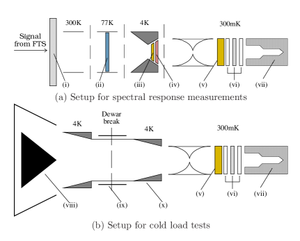
Detectors are optically characterized in two steps: one step measures the relative spectral response, and a second step measures the absolute power absorbed due to a known source. The absolute absorption efficiency is the normalization factor multiplying the relative spectral response that yields the measured absorbed power from the known source. The two optical setups are described below and illustrated in Fig. 5.
For both tests the optical setup at the detectors is the same. The detector absorber area is 10 mm in diameter. Preceding the detectors is a back-to-back Winston cone pair at 270 mK with a 10 mm diameter and A = 4.5 mm2-sr. This pair limits the radiation incident upon the detector to an angle of 7.5∘ which, according to simulations, does not significantly affect the detectors’ absorption spectra. A 6 mm gap separates the two detectors. To prevent interference from reflected radiation a terminating absorber with the shape shown in Fig. 5 is placed at the end of the stack. It is made from an absorptive epoxy similar to the coating on the cold load described in Subsection 4.B.1. Initial tests show evidence of high frequency absorption by the detectors. This is expected [1] and proposed FSB based instruments have provisions for optical low-pass filters ahead of the stack. A 6.6 mm piece of fluorogold[15] was placed in the light path following the Winston cone pair to absorb radiation above 750 GHz. The system is cooled to sub-Kelvin temperatures with a closed cycle 3He refrigerator.[16]
4.A Spectral response measurement
The spectral response measurements were conducted with a polarizing Michelson Fourier Transform Spectrometer (FTS) originally built as a prototype for the FIRAS experiment.[17] A 1200 K blackbody was used as the source of radiation. In addition to recording the spectrometer data, the blackbody was chopped at various frequencies to establish the effective detector time constants. While the measured frequency responses are used to interpret spectrometer data, all other measurements described here were conducted at frequencies low enough to be unaffected by the thermal response time. Fig. 5.a shows the optical setup used for this set of measurements.
The FSBs are designed for small radiative loads. To reduce the incident radiation to a level acceptable for the detectors, a neutral density filter (NDF) with a flat transmission level of 1.3% over a broad frequency range is placed in front of the detectors. The incident radiation passes through a straight cone pair at 4.2 K that acts as an A restrictor and reduces the light pipe diameter to 10 mm. To reduce the infrared radiative load on the cryostat, the straight cone pair holds a thin piece of fluorogold and a thin piece of Teflon foam[18]. These low-pass filters will marginally affect radiation at the two detector bands primarily through the interference spectrum caused by internal and external reflections at the filter surfaces (channel spectrum).
4.B Optical absorption measurement
4.B.1 Setup
To measure their response to changes in incident radiation, the detectors were illuminated with a variable temperature black-body source previously used for the same purpose in the TopHat experiment.[19] The source consists of two concentric cone-shaped cavities with internal walls shaped to enhance the number of scatterings of incoming rays. The internal walls are coated with a 1 mm thick layer of Eccosorb CR-114[20], an absorber of radiation within the band of interest.[21] Ray trace calculations using the source geometry and absorber properties show that the source is black to within one part in over this frequency range. Therefore, we do not include an error due to its non-unit emissivity. The source is mounted on a separate cryostat (cooled to 4.2 K) and connected to the detector cryostat with no partitioning window and a common vacuum. The light piping configuration is illustrated in Fig. 5.b.
The source temperature is controlled with heaters attached to its back end. The source is mechanically mounted on the 4.2 K plate by G-10 struts and thermally attached to it with two Pb straps. The source can be heated to 30 K without exhausting the liquid 4He bath too quickly. Source temperature modulations greater than 100 mK are possible at frequencies below 0.2 Hz. Two diode thermometers at different ends of the source agree within their ratings and show no phase difference during the modulations indicating that the source is isothermal at these frequencies. At these frequencies the bolometer signal is also in phase with the temperatures (see Fig. 7).
4.B.2 Measurements
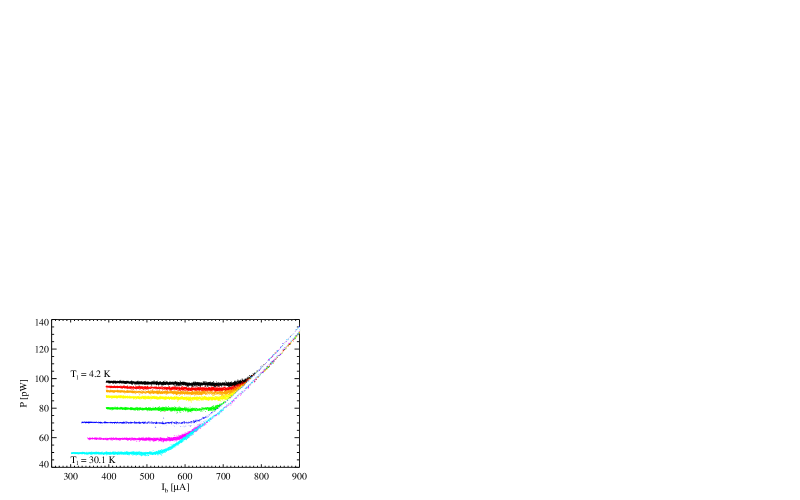
Changes in the power absorbed by each detector due to source temperature variations are measured using two methods. First, detector load curves are made at several source temperatures by varying the bias current and recording both the bias current and TES current (denoted and respectively in Fig. 4). The bias current is varied slowly so each data point represents an equilibrium condition. Fig. 6 shows the electrical power dissipated in the TES, computed from the measured currents, as a function of bias current for several black-body temperatures.
The general shape of these curves can be understood through the static thermal picture of Eq. (1) because the TES is in equilibrium at every bias current. The regions with flat electrical power correspond to the TES being in its transition. The power changes very little because, with held constant (for each curve), it simply reflects the small change in the r.h.s. of Eq. (1) as the TES traverses the narrow transition. The region where power increases quadratically is due to the TES behaving as a pure resistor when normal (). The superconducting region is not probed in these curves.
The flat regions assume different values for different source temperatures because changes in must cancel changes in at a given TES temperature. We compute the changes in absorbed radiation () due to changes in source temperature by measuring differences in electrical power () and using Eq. (2). This method allows a measure of only changes in optical power, not the absolute value of at any particular source temperature.
The electrical power () dissipated within the TES transition does vary slightly due to the finite transition width. Therefore we only use data from a 5 m span around a particular TES resistance from each load curve. If is uniquely determined by , selecting data in this way ensures that the r.h.s. of Eq. (1) is constant over the data sets. However, has a small dependence on . Because is not well known for TESs, we do not correct for this effect but estimate an error due to ignoring it by assuming that the chosen resistance contour has the same shape as the critical current curve of a superconductor on the plane.
To solve for absorbed optical power differences using Eq. (2), thermal conductances and must be known. Based on the thermal conductivity of Si3N4 and the geometry, is estimated at 21 nW/K with a large (50%) uncertainty. To obtain , the TES-to-stage thermal conductance was measured using a separate set of load-curve data in which only the cold stage temperature is varied between load curves. The measured thermal conductance, which includes both paths between TES 1 and the cold stage in Fig. 3.c, is close to because is substantially larger than . We find that the factor between and is only important for the detectors with Ti-Al-Ti leads ( 2.5 nW/K) and unimportant for the ones with Mo leads ( 0.7 nW/K). Even for the former, . Thus the large uncertainty in only introduces a small error in the final results.
In the second method for measuring detector response to source temperature changes, the source temperature was slowly modulated by hundreds of mK with a constant bias applied to the TES. Fig. 7 shows both source temperature and TES current versus time. Eq. (1) when used to describe this equilibrium situation yields as the detectors’ static response
| (3) |
where and .
In the denominator of Eq. (3), the ratio of the first term to the second is the loop gain of the electro-thermal feedback. As verified with load-curve data, this ratio is large for the bias points used because each detector was biased within the lower 70% of its transition. Therefore, the second term in the denominator is ignored when is converted to for use in Eq. (2) to evaluate . Typically, the fractional error due to this simplification is 3%. Although the effects of additional resistance in series with the TES are not included in Eq. (3), we calculate an error due to the measured sub-m series resistance.
5 Prototype optical characteristics
5.A Spectral response
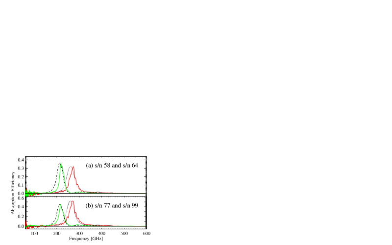
The shape of the radiation spectrum absorbed by a detector is measured using the methods described in section 4.A. To obtain the relative spectral response of detectors we divide the measured profile by a spectrum due to the 1200 K blackbody, cut off at high-frequency by the fluorogold filters. We ignore the channel spectra of all filters when dividing out the incident spectrum due to uncertainties in thickness and spacing of filters and because unanticipated channel spectra, from gaps in light piping for example, may be present in the incident radiation. Fig. 8 shows the relative spectral response of detectors calculated in this way.
The residual antisymmetric component of interferograms is used to calculate the uncertainty in the absorption profiles and represented in Fig. 8 by the line thickness. This uncertainty accounts for the noise level at each frequency as well as systematics due to the signal not being perfectly symmetrized. The uncertainties indicated in Fig. 8 are small in the resonance regions and only become significant at low frequencies due to noise. Spectral shapes of Fig. 8 are not completely accurate representations of the intrinsic detector spectral response for two reasons. 1) The channel spectra in the incident radiation have not been divided out; the dominant “ripple” pattern seen on the curves can be attributed to the thick (6.6 mm) fluorogold filter based on its period. However, the overall shapes of these curves may be affected by longer period channel spectra from thinner filters. But the magnitude of such effects cannot be much greater than that of the dominant channel spectrum from the thick fluorogold filter because the relevant indices of refraction are no greater than that of fluorogold. 2) The notch in the incident spectrum due to the 271 GHz detector has not been divided out of the 219 GHz detector’s profile. This effect is clear in Fig. 8 where a dip to near zero absorption occurs in the 219 GHz detector at the resonance of the preceding detector.
The small differences in shape between the two 271 GHz detectors are on the order of the differences one would expect due to thin-filter channel spectra dissimilarities between the two setups. However, one of the 219 GHz detectors has a 1% (apparently uniform) level of continuum absorption above the resonance, not seen in the other similar detector. We do not know the behavior of this continuum above 800 GHz due to the low-pass filters in the setup. We know that it is not an analysis artifact because this continuum absorption shows a dip at 560 GHz, expected due to water vapor absorption in the spectrometer. An inspection of detectors showed the absorber-backshort separation was greater by about 15% of the target value in this device, possibly due to adhesive between the frames peeling off, whereas the spacing was accurate to within 2% in the other FSBs.
Fig. 8 also shows HFSS models of the two FSB channels. The model curves have been scaled from their peak absorption near 80% to match the measured curves at the resonance peaks. The measured absorption profiles are slightly narrower than model predictions with Q values ranging from 9 to 11, but are still well suited for use in ground based instruments like the SPEED camera that utilize the mm-wave transmission windows of the atmosphere. The results described thus far constrain only the relative optical absorption as a function of frequency. The next section explains how the absolute scale factor for the curves of Fig. 8 was established.
5.B Absolute absorption efficiency
Under the assumption of a perfect black body, the measured response of intervening filters, and the design A of the Winston cone pair, we calculate , the total amount of radiated power from the source incident on the detector stack at a particular source temperature as a function of frequency. The amount of power absorbed by the detector due to the source is then
| (4) |
Here is the measured relative absorption profile of a detector normalized so that its peak is at unity and is the true fraction of incident power absorbed at the peak.
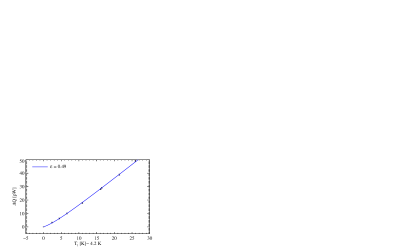
Fig. 9 shows data from the load curve method described in section 4.B.2 along with a curve showing the r.h.s. of Eq. (4) for the efficiency () that best fits the data. The data and calculated values are offset to reflect only changes in power due to source temperature changes from 4.2 K. Data from the source-temperature-modulation method are used similarly to estimate efficiency. Both methods yield good quality fits to data within errors, as in Fig. 9, indicating that no major effects are being missed by this simple analysis.
The efficiencies for each detector obtained through both methods are summarized in Table 2. While both methods were used at both test facilities, the load curve (“DC tests”) results presented here are obtained from one setup while the source modulation (“AC tests”) results are taken from the other. The general trend of AC efficiencies being higher than DC efficiencies is due to a difference between the two test facilities, not the difference in method, because results of the two methods from each test setup are in good agreement. We show results from both setups to bring attention to this trend which at the moment remains unexplained and is likely due to differences in light piping and filter setups.
We also do not understand why the measured efficiencies ranging from 20% to 60% do not agree with the higher levels of 80% predicted by simulations. We do not focus on this discrepancy because we have not independently assessed the performance of models in predicting absolute absorption efficiency. On the other had, we did expect the good agreement seen between models and measurement in terms of spectral profiles, based on measured transmission spectra of single FSB layers at room temperature. The true resistivity of the gold on the absorbing layer has not been measured. A difference from the ideal value (1.6 /square) by a factor of a few could also explain the discrepancy. We have also ignored waveguide-like effects of the Winston horns treating them as pure A limiters that transmit 2.4 spatial modes at 219 GHz and and 3.7 modes at 271 GHz. While the limiting approach angle to the FSBs of 7.5∘ causes an insignificant deviation from the modeled absorption (according to simulations), attenuation of spatial modes may result in losses as high as 20% given the 1.35 mm-diameter small orifice and the gradual narrowing of the horn prior to it. Because we ignore this effect, formally, the absolute absorption efficiencies () quoted here are for FSBs that couple to radiation through a 4.5 mm2-sr back-to-back Winston horn pair, a likely design for an instrument such as the SPEED camera.
The error due to noise in the measurements (statistical error) is small compared to estimates of systematic error. Systematic errors fall into two categories: errors in calculating the amount of radiation power incident on detectors and errors in using detector signals to estimate differences in absorbed power. In calculating the amount of incident optical power, uncertainties due to absolute and differential thermometry errors of the source temperature are included. The transmission spectra of filters are necessary only in the cases where different filters were used between the spectral response and cold load tests. Because there were such changes, we measured the cold (4.2 K) transmission properties of the relevant filters using a filter wheel setup to check the accuracy of their transmission models.[22] We also calculate an error due to ignoring differences in channel spectra between the spectral-response and cold-load measurements. We attribute a further 10% error in the incident optical power to non-idealities of the light pipes and Winston cones. While no account is made for changes in optical power from sources other than the cold load during our tests, we estimate the absorption due to such sources to be no more 20 pW in most of our tests.
As for systematics in interpreting detector signals, the value and standard deviation of a large sample of nominally 6 m shunt resistors () was established at 4.2 K and used in the analysis. As described in section 4.B.2, we account for errors in the relevant thermal conductances and for ignoring the current dependence of TES resistance. For the AC tests, we estimate an error due to finite loop gain of the electro-thermal feedback. We also include errors due to possible misassignment of stray resistance in series with the TES as on disk or off disk (i.e. whether the bolometer is heated or not heated due to power dissipated through that resistance). A 1% error in all gain factors in the cold and warm electronics is also assumed.
6 Conclusion
Tests of the prototype devices demonstrate that the FSB concept can be realized with input from simulations to reliably set spectral characteristics and that FSBs can be fabricated with reproducible performance. Because the detectors can be arranged in a stack with high out-of-band transmission, individual channels have absolute efficiencies comparable to the best seen in conventional bolometers placed behind band defining filters.[23, 24] The measured spectral profiles permit up to 8 simultaneous minimally overlapping channels between 150-1500 GHz, a frequency range with much potential for characterizing many interesting astronomical sources and the backgrounds/foregrounds to those sources. At present, there is evidence that internal thermal couplings within detectors need improvement. More work is needed to understand the thermal and noise properties of these detectors. Another area of future research is the use of FSBs with patterns of bars, not crosses, for polarization sensitive measurements.
Acknowledgments
This work is supported by NASA grant S20052896400000 and the Five College Radio Astronomy Observatory under NSF grant AST-0228993. The FSB devices were fabricated using the exceptional facilities of the Detector Development Laboratory at NASA/GSFC.
References
- [1] M. S. Kowitt, D. J. Fixsen, A. Goldin, and S. S. Meyer, “Frequency Selective Bolometers,” Appl. Opt. 35, 5630 (1996).
- [2] G. Wilson, T. C. Chen, E. S. Cheng, D. A. Cottingham, T. Crawford, D. J. Fixsen, F. M. Finkbeiner, D. W. Logan, S. Meyer, R. F. Silverberg, and P. T. Timbie, “Spectral energy distribution camera for the LMT,” in Millimeter and Submillimeter Detectors for Astronomy. Edited by Phillips, Thomas G.; Zmuidzinas, Jonas. Proceedings of the SPIE, Volume 4855, pp. 583–593 (2003).
- [3] R. F. Silverberg, B. Campano, T. C. Chen, E. Cheng, D. A. Cottingham, T. M. Crawford, T. Downes, F. M. Finkbeiner, D. J. Fixsen, D. Logan, S. S. Meyer, T. Perera, E. H. Sharp, and G. W. Wilson, “A bolometer array for the SPEctral Energy Distribution (SPEED) Camera,” in Astronomical Structures and Mechanisms Technology. Edited by Antebi, Joseph; Lemke, Dietrich. Proceedings of the SPIE, Volume 5498, pp. 659–666 (2004).
- [4] B. Munk, Frequency Selective Surfaces: Theory and Design (John Wiley & Sons, Inc., 2000).
- [5] S. T. Chase and R. D. Joseph, “Resonant array bandpass filters for the far infrared,” Appl. Opt. 22, 1775–1779 (1983).
- [6] H. Severin, “Nonreflecting absorbers for microwave radiation,” IRE Transactions on Antennas and Propagation 4, 385–392 (1956).
- [7] Ansoft, “High Frequency Structure Simulator v. 8.5,” 225 West Station Square Drive, Suite 200, Pittsburgh, PA, 15219, USA.
- [8] E. L. Pelton and B. A. Munk, “Scattering from periodic arrays of crossed dipoles,” IEEE Transactions on Antennas and Propagation 27, 323–330 (1979).
- [9] J.-Y. Wu, D. M. Kingsland, J.-F. Lee, and R. Lee, “A Comparison of Anisotropic PML to Berenger’s PML and Its Application to the Finite-Element Method for EM Scattering,” IEEE Transactions on Antennas and Propagation 45, 40–50 (1995).
- [10] J.-P. Berenger, “Three-Dimensional Perfectly Matched Layer for the Absorption of Electromagnetic Waves,” Journal of Computational Physics 127, 363–379 (1996).
- [11] F. M. Finkbeiner, T. C. Chen, S. Aslam, E. Figueroa-Feliciano, R. L. Kelley, M. Li, D. B. Mott, C. K. Stahle, and C. M. Stahle, “Fabrication of Superconducting Bilayer Transition Edge Thermometers and their Application for Spacebourne X-ray Microcalorimetry,” IEEE Transactions on Applied Superconductivity 9, 2940–2942 (1999).
- [12] T. C. Chen, A. Bier, B. A. Campano, D. A. Cottingham, F. M. Finkbeiner, C. O’dell, E. Sharp, R. F. Silverberg, and G. Wilson, “Development of molybdenum-gold proximity bilayers as transition edge sensors for the SPEED camera,” Nuclear Instruments and Methods in Physics Research A 520, 446–448 (2004).
- [13] J. A. Chervenak, K. D. Irwin, E. N. Grossman, J. M. Martinis, C. D. Reintsema, and M. E. Huber, “Superconducting multiplexer for arrays of transition edge sensors,” Appl. Phys. Lett. 74, 4043 (1999).
- [14] D. A. Cottingham, A. Bier, B. Campano, T. C. Chen, E. S. Cheng, T. Crawford, F. M. Finkbeiner, D. J. Fixsen, D. W. Logan, S. Meyer, E. Sharp, R. F. Silverberg, and G. Wilson, “Development of frequency selective bolometers for ground-based MM-wave astronomy,” in Millimeter and Submillimeter Detectors for Astronomy. Edited by Phillips, Thomas G.; Zmuidzinas, Jonas. Proceedings of the SPIE, Volume 4855, pp. 192–200 (2003).
- [15] Produced by E.I. duPont de Nemours & Co. Polytetrafluoroethylene (fluorogold) rod stock conforming to standard ASTM D1710.
- [16] R. S. Bhatia, S. T. Chase, S. F. Edgington, J. Glenn, W. C. Jones, A. E. Lange, B. Maffei, A. K. Mainzer, P. D. Mauskopf, B. J. Philhour, and B. K. Rownd, “A three-stage helium sorption refrigerator for cooling of infrared detectors to 280 mK,” Cryogenics 40, 685–691 (2000).
- [17] D. J. Fixsen, E. S. Cheng, D. A. Cottingham, R. E. Eplee, T. Hewagama, R. B. Isaacman, K. A. Jensen, J. C. Mather, D. L. Massa, S. S. Meyer, P. D. Noerdlinger, S. M. Read, L. P. Rosen, R. A. Shafer, A. R. Trenholme, R. Weiss, C. L. Bennett, N. W. Boggess, D. T. Wilkinson, and E. L. Wright, “Calibration of the COBE FIRAS instrument,” Astrophys. J. 420, 457–473 (1994).
- [18] Produced by W. L. Gore Associates. Part No. RA7957-3.
- [19] S. S. Cordone, “Intrumentation for Precision Measurements of Anisotropy in the Cosmic Microwave Background,” Ph.D. thesis, University of Wisconsin - Madison (2004).
- [20] Produced by Emerson & Cuming Microwave Products. Part No. CR-114.
- [21] H. Hemmati, J. C. Mather, and W. L. Eichorn, “Submillimeter and millimeter wave characterization of absorbing materials,” Applied Optics 24, 4489 (1985).
- [22] M. Halpern, H. Gush, E. Wishnow, and V. D. Cosmo, “Far-Infrared Transmission of Some Dielectrics at Cryogenic and Room Temperatures: Fluorogold, Ecosorb, Stycast, and Various Other Plastics,” Applied Optics 25, 565–570 (1986).
- [23] A. D. Turner, J. J. Bock, J. W. Beeman, J. Glenn, P. C. Hargrave, V. V. Hristov, H. T. Nguyen, F. Rahman, S. Sethuraman, and A. L. Woodcraft, “Silicon nitride Micromesh Bolometer Array for Submillimeter Astrophysics,” Applied Optics 40, 4921–4932 (2001).
- [24] W. S. Holland, C. R. Cunningham, W. K. Gear, T. Jenness, K. Laidlaw, J. F. Lightfoot, and E. I. Robson, “SCUBA - A submillimetre camera operating on the James Clerk Maxwell Telescope,” in Proc. SPIE Vol. 3357, p. 305-318, Advanced Technology MMW, Radio, and Terahertz Telescopes, T. G. Phillips, ed., pp. 305–318 (1998).
| [GHz] | [m] | [m] | [m] | s [m] |
|---|---|---|---|---|
| 219 | 572 | 14 | 1020 | 336 |
| 271 | 473 | 11.5 | 844 | 277 |
The columns, in order, are the center frequency (), the length and width of a dipole element ( and ), the repetition scale of the cross pattern (), and the spacing between absorber and backshort ().
| Detector | [GHz] | (%) | (%) |
|---|---|---|---|
| s/n 58 | 219 | 286 | 444 |
| s/n 64 | 271 | 245 | 394 |
| s/n 77 | 219 | 405 | 505 |
| s/n 99 | 271 | 497 | 555 |
The columns, in order, are the detector number, center frequency, the absorption efficiency as measured with load-curve data, and absorption efficiency as measured by modulating the source temperature.
List of Figure Captions
Fig. 1. Cartoon of a stack of two FSBs. Of the radiation entering from the left, the component in the band of FSB 1 (dotted arrows) is absorbed and radiation outside that band passes through the detector. Of the remaining light, radiation that is within the band of FSB 2 (solid arrows) is absorbed and all other radiation (dashed arrows) continues down the stack until absorbed by an additional FSB or by a terminating absorber. On the right side is a cartoon illustrating the combination of absorbing layer and reflecting backshort.
Fig. 2. FSB surface geometry.
Fig. 3. (a) Picture of complete FSB absorber frame. (b) Close-up showing TES and leads. (c) Simple model describing the static thermal behavior of detectors. represents heat conductance from the TES to the cold stage. represents the gold-ring-to-TES thermal conductance (see section 3). The arrows indicate the physical locations of elements in the schematic model and thermal links between them. corresponds to the small gap seen in (b) between the TES and the “stub” extending off the gold ring.
Fig. 4. The TES is biased by running a current () through the shunt-TES combination. The current flowing through the TES () is measured with a SQUID multiplexer.
Fig. 5. In both experimental arrangements light pipes are attached to the several temperature stages of the cryostat and filters are attached to the light pipes. (i) Polypropylene window (0.25 mm) at room temperature (ii) 1.3% flat transmission Neutral Density Filter (iii) 1.6 mm fluorogold (iv) 3.2 mm Teflon foam (Gore-tex) (v) 6.6 mm fluorogold (vi) 2 FSBs with a 6 mm gap (vii) Cavity made of magnetically loaded epoxy to absorb transmitted radiation. (viii) Blackbody source capable of temperatures from 4-40 K housed in separate cryostat with shared vacuum (ix) 77 K shielding around (x) 4.2 K light pipe.
Fig. 6. Electrical power dissipated in a 271 GHz detector at various source temperatures from 4.2 K to 30.1 K. The electrical power within the transition (flat region) decreases with increasing source temperature.
Fig. 7. The solid curve is the measured source temperature modulation. The plus signs are measured values of the TES current for a 271 GHz detector. At this slow modulation speed, the source temperature and bolometer response are in phase (the TES current is AC coupled and 180∘ out of phase with bolometer loading).
Fig. 8. Solid lines show the spectral response of the two FSB stacks. The difference between the two stacks is in the TES lead material which should not affect optical characteristics. In each stack, the 219 GHz detector is placed down stream of the 271 GHz detector in the light path. The line thickness of each curve represents the uncertainty when it exceeds the constant line thickness used to represent the data (mainly at low frequencies). Overlaid with dashed and dotted lines are the corresponding HFSS models scaled to have the same peak absorption as the data.
Fig. 9. Estimate of absorbed optical power versus source temperature for a 271 GHz detector. The curve through the data is the r.h.s. of Eq. (4) scaled to best fit the data. The value of the best fit efficiency is also indicated. The indicated error bars are statistical. The error from the fit is combined with further systematics to get the final uncertainties of Table 2