An Active Gain-control System for Avalanche Photo-Diodes under Moderate Temperature Variations
Abstract
Avalanche photodiodes (APDs) are promising light sensor for various fields of experimental physics. It has been argued, however, that variation of APD gain with temperature could be a serious problem preventing APDs from replacing traditional photomultiplier tubes (PMTs) in some applications. Here we develop an active gain-control system to keep the APD gain stable under moderate temperature variations. As a performance demonstration of the proposed system, we have tested the response of a scintillation photon detector consisting of a 55 mm2 reverse-type APD optically coupled with a CsI(Tl) crystal. We show that the APD gain was successfully controlled under a temperature variation of = 20∘C, within a time-cycle of 6000 sec. The best FWHM energy resolution of 6.10.2 was obtained for 662 keV -rays, and the energy threshold was as low as 6.5 keV, by integrating data from +20∘C 0∘C cycles. The corresponding values for 20∘C 0∘C cycles were 6.90.2 and 5.2 keV, respectively. These results are comparable, or only slightly worse than that obtained at a fixed temperature. Our results suggest new potential uses for APDs in various space researches and nuclear physics. As examples, we briefly introduce the and Cute-1.7 satellite missions that will carry the APDs as scientific instruments for the first time.
keywords:
avalanche photodiode, -rays, gain-control, scintillation detectionPACS:
07.85; 95.55.A; 85.60.D, , , , , , , , , and
1 introduction
Silicon avalanche photodiodes (APD;[1] see also [2, 3, 4, 5, 6, 7, 8]) are the only devices which have internal gain. Since the good features of both photodiodes (PDs) and photomultiplier tubes (PMTs) are shared in a single device, APDs offer new design for physics experiments and devices for nuclear medicine. In our previous works, we have studied the performance of reverse-type APDs111We note that the reverse-type APD refers to a reach-through design where the narrow, high-field multiplication region is near the front of the device [9, 10]. as an X-ray/-ray detector optically coupled with various inorganic scintillators, such as CsI(Tl), BGO, GSO(Ce), and YAP(Ce) [9, 10]. Thanks to its high quantum efficiency (QE) and low noise contribution, reverse-type APDs generally show much better energy resolution than traditional PMTs. Moreover, due to their internal gain of 50 or more, we have successfully used these APDs to detect weak scintillation light from CsI(Tl) crystal at energies as low as 5 keV even at room temperature. Most recently, we have successfully developed various large area reverse-type APDs with Hamamatsu Photonics, up to 2020 mm2 square area[11]. This is the one of the largest monolithic APD pixel ever produced. Such large dimensions have been awaited by researchers world-wide, and further extend the potential of APDs for various applications in the near future.
It should be noted, however, that the gain characteristics of APDs depend on both the bias voltage and the temperature. Although the gain variation of APDs on bias voltage ( 3/V at a gain of 50) is only two times larger than the voltage coefficient of typical PMTs, the temperature variation can be a more critical problem for APDs. When the APD device is cooled, the bias voltage required to achieve a certain gain is significantly reduced. This is due to the much smaller probability of electron energy loss in interactions with phonons as compared with that at room temperature. In fact, the temperature coefficient of APDs ( 2/∘C) is about ten times larger than that of typical PMTs[7, 9]. Therefore, in order to stabilize the gain at the 1 level, the temperature must be controlled within 0.5∘C, which is often too severe a requirement for detectors used in space missions, and for the large calorimeters used in the accelerator experiments. It should be noted that the temperature variation is very rapid in most of the cases discussed above. For example, temperatures of detectors in satellites or balloon experiments can vary by a large amount, but typically 20∘/hour (e.g., http://lss.mes.titech.ac.jp/ssp/cubesat/index_e.html for the Tokyo Tech pico-satellite CUTE-I). Such requirements are generally much less stringent for ground-based experiments.
In order to stabilize the gain of an APD detector against temperature variations, a number of authors have proposed different ideas to meet their specific purposes. For example, it has been argued that the temperature compensatation should keep the APD performance near the best multiplication factor defined as the highest signal-to-noise ratio ([12], see also [13]). This is a very simple design using a feedback loop of analog electronics, where an appropriate bias voltage is automatically generated at different temperatures. An obvious weakness is that the bias is corrected only linearly against the temperature ( ), which is not generally true in usual applications (see also 2.1 and Figure 4()). Such a non-linearity was carefully considered by different authors [14] but required careful tuning of circuit parameters used in the gain control system, a time-consuming process, especially when the responses of individual APDs can differ significantly. These authors have mentioned that they are currently developing a more convenient system using a CPU, where the temperature compensation can be easily done by a software program. Apparently, such a CPU-based system is much more flexible and makes it easier to include any irregularities and non-linearities in the APD gain characteristics.
In this paper, we present a novel, CPU-based design to keep the APD gain stable under moderate temperature variations. The paper is organized as follows. In 2, we show the gain characteristics of an APD to explain the basic concept of active gain-control system. As a performance demonstration of the proposed system, we have made a scintillation photon detector consisting of a 55 mm2 reverse-type APD optically coupled with a CsI(Tl) crystal. In 3, we demonstrate that our system works well under moderate temperature variations between 20∘C and 0∘C, or +20∘C and 0∘C, in a 6000 sec time-cycle. In 4, we briefly introduce the applications of our system for the future space missions and Cute-1.7, both of which will carry APDs as a scientific instrument. We also comment on the further potential of using an active gain-control system in ground based experiments. Our results are summarized in 5.
2 Development of Active Gain-Control System
2.1 APD Gain Characteristics
We used a reverse-type APD of 55 mm2 surface area, recently developed by Hamamatsu Photonics K.K. (Hamamatsu S8664-55). Full details of the detector performance and the internal structure of S8664-55 are given in the literature [7, 10, 11]. Summarizing the parameters of the APD assembled in this experiment, the leakage current is 1.52 nA and the detector capacitance is 85 pF when fully depleting the device. An avalanche gain of 50 is achieved for a bias voltage of 370 V and the breakdown takes place at 411 V. All these parameters were measured at room temperature (+25 ∘C). Here we particularly focus on the APD gain characteristic to explain the basic concept of the gain-control system described in detail in following sections.
The APD gain, , can be measured under constant illumination of a monochromatic light source by recording the photocurrent of the APD as a function of bias voltage. We use a light-emitting diode (LED) emitting at 5255 nm. This wavelength is particularly important to mimic the scintillation light from CsI(Tl) crystal (550 nm) as we will see in Section 3. At voltages lower than 50 V, the APD gain can be regarded as unity. Figure 1 () shows variations of APD gain as a function of bias voltage for different temperatures (measured from 20∘C to +20∘C). At +20∘C, the gain reaches 30 at 353 V, whereas only 320 V is necessary to obtain the same gain in an environment cooled to 20∘C. Such a characteristic is more clearly seen in Figure 1 (), where the APD gains for fixed bias voltages are plotted as a function of temperature. At a gain of =30 and a temperature of =0∘C, the gain variation is approximated by
| (1) |
which is quite large compared to that of usual PMTs, but is the comparable to reverse-type APDs reported in the literature[7]. Under the conditions =30 and =0∘C, the dependence of gain on bias voltage can be approximated by
| (2) |
Note, this is a relation assuming an exponential change of APD gain with bias voltage. It can be seen that this is an over-simplified model as there is a clear deviation from a straight-line in the semi-log plot of Figure 1 (). Nevertheless, this provides a convenient way of comparing the APD performance with those of others in the literature [7, 8, 9].
An important remark on Figure 1 () is that, for a fixed APD gain (e.g., dashed line shows =30 line), there exists a one-to-one relation between the bias voltage and the temperature. In other words, we can determine the bias voltage that produces for an arbitrary temperature. This is a for the gain-control system discussed below. If the temperature increase by , then the APD gain should decrease by when the bias voltage is fixed to a constant value. In order to restore the original APD gain, we can simply increase the bias voltage, by V, to cancel out the gain reduction. From equation (1) and (2), and are related by = , where is a constant but depends on the temperature and the APD gain.


2.2 System Design
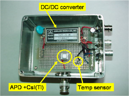
As a performance demonstration of the proposed idea, we made a scintillation photon detector consisting of a reverse-type APD (S8664-55; see above) optically coupled with a cubic CsI(Tl) crystal of dimensions 555mm3. Figure 2 shows a picture of the “sensor box”, where the APD scintillation detector, a DC/DC converter (Analog Modules; Model 521-5) and a temperature sensor (Analog Device: AD590) are all implemented in a single metal box. The DC/DC converter outputs a 0600 V bias voltage to the APD, by a factor of 120 amplification of the input DC signal (from 0 to 5 V maximum). The AD590 is a 2-terminal circuit temperature transducer that produces an output current proportional to absolute temperature (1 A/K). The separation between the APD sensor (APD+CsI(Tl)) and AD590 is about 1.5 cm.
The method of gain-control is straightforward. First, one should define a reference table or empirical function of bias voltage as a function of temperature to stabilize the detector gain. Second, the detector temperature should be monitored with an appropriate time interval, . For example, if the temperature variation is expected on hour scales, it is recommended to monitor AD590 output every minute, or on even shorter time scales. Third, the optimum voltage to keep the detector gain constant is calculated, and the APD bias changed if necessary. Automatic iteration of these processes every results in a robust gain-control system under the moderate temperature variations.
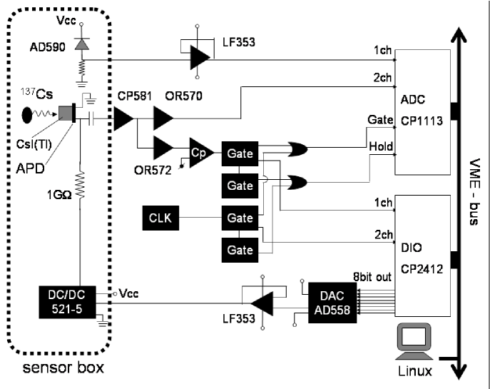
The block diagram of the system developed in this paper is shown in Figure 3. The signals from the APD and the temperature sensor were read by a peak-hold 12-bit ADC (Clearpulse; CP1113A) connected to a Linux computer via a VME bus. The output signals from the APD were amplified by a charge sensitive preamplifier (Clearpulse; CP581K) and fed to the shaping amplifiers (ORTEC; 570 and 572), where in the latter, fast shaping is used to trigger the data acquisition. The DC output of AD590 was monitored every 1 sec, and then appropriate bias voltage is calculated as a function of temperature, in the DAQ program. This bias voltage is output from the VME DIO (Clearpulse; CP2412) as 8-bit digital data, and fed to the DAC (Analog Device: AD558) input. The maximum output of the DAC is allowed in the range 2.5510 V. Here we set the maximum voltage to 3.33 V, in order that the maximum of DC/DC converter (Analog Modules; 521-5M) becomes 3.33 V 120 = 400V. Therefore a 1 bit input to the DAC corresponds to 13.0mV120 = 1.56 V when output from the DC/DC converter. Note this may produce 3.9 fluctuations in APD gain if = 30 (see 2.1). We will revisit this problem in 4.2
3 Performance Test
3.1 Calibration
Prior to the performance test, we first calibrated the APD + CsI(Tl) system to obtain an empirical relation between the bias voltage and the temperature. As a reference, we measured a spectrum of 137Cs -rays at 20∘C. The corresponding APD gain is =30. We then calibrated the system by measuring the peak of 662 keV -rays every 2∘C from 20∘C to +20∘C. Actually, we only measured the bias voltage that makes the 662 keV peak ADC channel equal to that obtained for 20∘C, under various temperatures. Note, in this system, we do not measure the shift of APD gain itself as described in Figure 1 (), but the light yield of a CsI(Tl) crystal read through the APD. A great merit of this method is that we can correct not only the variations of APD gain, but the response of the CsI(Tl) at the same time. In fact, it is known that the light yield of CsI(Tl) scintillator measured at 20∘C decreases by 15 from that measured in 20∘C (e.g., http://www.scionixusa.com/pages/navbar/scin_crystals.html). Although a wide variety exists in response of various scintillators, our approach is always applicable in correcting the APD gain the scintillator. Figure 4 () shows the required bias voltage thus obtained, to keep the gain of scintillation detector as a whole, under various temperatures. Figure 4 () shows the AD590 output (ADC channel; 2.5mV/ch) as a function of temperature. From these two figures, we obtained an empirical, approximate relation between the bias voltage () and the AD590 output () as;
| (3) |
This is further converted to the input channel of DAC (AD558) via the relation
| (4) |
where we only take the integral part of the right-hand side in equation (4). Therefore, by measuring the ADC channel of temperature sensor , we can uniquely define an appropriate bias voltage to keep the detector gain constant every one second.


3.2 Active Gain-Control in +20∘C 0∘C Cycles
As a performance demonstration of an active gain-control system, we measured the 662 keV -ray spectrum under moderate temperature variations. The temperature was controlled with a thermostat to vary between +20∘C and 0∘C, in a time-cycle of 6000 sec. This time constant and the temperature range is particularly selected from the observation and the simulation results for the small cubic satellite missions in low-Earth orbit (CUTE-1 and Cute-1.7; see 4.1 and [19]). Figure 5 () shows a time history of temperature variations in the thermostat (two cycles; thin dashes), overlaid with the measured temperature variation reconstructed from AD590 data (thick line). Due to the heat capacitance of the sensor box (Figure 2), the temperature variations of APD lags behind that in the thermostat for 600800 sec. Also, the minimum and the maximum temperature during the cycle is +4∘C and +16∘C, except for the very first phase of temperature cycle starting from +20∘C.
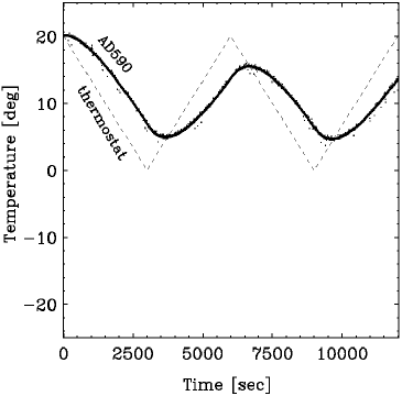

Figure 5 ( upper) shows a 662 keV -ray spectrum integrated over two temperature cycles (12000 sec, Figure 5) measured with the active gain-control system. The energy resolution and the threshold are 6.1 and 6.5 keV, respectively. Note that, these values are comparable with those measured at a temperature. For example, the corresponding energy resolutions are 5.6 (+20∘C) and 5.7 (0∘C) and the energy thresholds are 7.1 keV (+20∘C) and 6.1 keV (0∘C), respectively. To demonstrate the merits of our system more clearly, we also measured a 662 keV -ray spectrum integrated over the same temperature cycles, the active gain-control (with the bias voltage is fixed to 332.5V). As shown in Figure 6 (; bottom), the spectrum is significantly distorted, so much so that the 662 keV peak has become a plateau rather than having a single Gaussian form. Therefore we confirm that the active gain-control system described in this paper provides effective feedback to stabilize the APD gain, at least under moderate temperature variations.
3.3 Active Gain-Control in 20∘C 0∘C Cycles
Next we measured the 662 keV -ray spectrum in a lower temperature cycle, between 20∘C and 0∘C. As for the previous section, the temperature was controlled with a thermostat and slowly varied on a time scale of 6000 sec (time period for one cycle). Figure 6 () shows a time history of temperature cycles in the thermostat (two cycles; thin dashes), overlaid with a measured temperature variation reconstructed from AD590 data (thick line). Again, the temperature variation of the APD lags behind that in the thermostat by 600800 sec. The actual minimum and the maximum temperature of sensor during the cycle is 16∘C and 4∘C, except for the very first phase of temperature cycle starting from 0∘C.
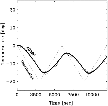

Figure 6 ( upper) shows a 662 keV -ray spectrum integrated over two temperature cycles (12000 sec, Figure 6) measured with the active gain-control system. The energy resolution and the threshold are 6.9 and 5.2 keV, respectively. For comparison, the corresponding energy resolutions are 6.3 (20∘C) and 5.7 (0∘C) and energy thresholds are 5.1 keV (+20∘C) and 6.1 keV (0∘C), respectively, for fixed temperatures. Similar to Figure 5 (), we compared a 662 keV -ray spectrum integrated over the same temperature cycles, the active gain-control (with the bias voltage is fixed to 320.0 V). Again we can see in Figure 6 (; bottom) that the spectrum is significantly distorted. Such gain fluctuations are successfully reduced with the use of the active gain-control system.
From Table 1, we see that the energy threshold decreases with temperature, as has been discussed elsewhere [7]. The sources of dark noise in an APD are divided into “dark current noise” and “capacitance noise”, where the former is predominant for S8664-55 (e.g., [11]). Therefore significant reduction of dark current at lower temperature ([7]) improves the energy threshold as given in Table 1. Meanwhile, the energy resolution is worst at 20 ∘C. As briefly notified in 3.1, the light yield of CsI(Tl) scintillator decreases with temperature. Assuming the energy resolution of CsI(Tl) is related to the incident -ray energy as , one should expect a 10 broadening in the energy resolution. This is indeed what we see in Table 1, but of curse, more careful consideration including the intrinsic resolution of scintillation crystal [5] is necessary for further clarification.
| Temperature | Condition | Energy Resolution | Energy Threshold |
|---|---|---|---|
| (FWHM, @662keV) | |||
| +20 0 ∘C | 2-cycles | 6.1 | 6.5 keV |
| 20 0 ∘C | 2-cycles | 6.9 | 5.2 keV |
| +20∘C | fixed | 5.6 | 7.1 keV |
| 0∘C | fixed | 5.7 | 6.1 keV |
| 20∘C | fixed | 6.3 | 5.1 keV |
4 Future Plans
4.1 Applications in Space Satellite Missions
Let us briefly review the advantages of using APDs. APDs are very compact and have rugged structures. They can be operated under relatively low bias voltages, and are less affected by magnetic fields. Moreover, the internal gain and high QE are great merits in detecting weak scintillation light, as well as direct detections of soft X-rays and low energy charged particles [10]. We have a plan to use APDs for the X-ray/-ray observation satellite , which is a planned Japanese satellite which could be launched as early as 2011[15, 16]. Although detailed design parameters are still being discussed, will have a height of 13 m, a diameter of 2.2 m, and a total mass of 1800 kg. In this mission, reverse-type APDs will be implemented as a light sensor for large BGO plates and blocks, that effectively reject background cosmic rays and atmospheric -rays [9]. A typical orbit for Japanese X-ray missions is a low-Earth, circular trajectory with an altitude of 500600 km. The inclination and the orbit cycle would be 31∘ and 6000 sec, respectively. In such orbits, the detector temperature is easily controlled within a range of 155 ∘C, without the aid of an additional heater or thermostat. Therefore the expected temperature variation is quite similar to the range we have tested in 3.3.
It is, however, noted that APDs have not previously been used in the space environment as a radiation detector. In general, semiconductor devices experience a degeneration of performance as the total radiation dose increases. We have therefore conducted a proton beam test to carefully estimate the radiation effects caused by high energy charged particles in orbit, and found that reverse-type APDs are sufficiently tolerant to be used in low-Earth orbit[17]. For further qualification tests, we will carry the same reverse-type APD onboard the forthcoming pico-satellite Cute-1.7. We will examine the active gain-control system on-board using a personal digital assistant (PDA) for the first time in space [18]. A detailed report for the expected APD performance in orbit is given elsewhere [19].
4.2 Further Comments on Active Gain-Control System
The original motivation of developing the gain-control system was to use the APD in satellite missions, where significant temperature variation is inevitable. However, this same system can be of course useful in various ground-based experiments. For example, in the field of particle physics, it is quite difficult to maintain a whole detector system (e.g., large scintillation calorimeters surrounding an accelerator) at the same temperature. Fortunately, in most cases, temperature variation is not as large as in a space environment, and variability occurs on relatively longer time scales (e.g., a few hours to days). Therefore, the monitoring the temperatures at various detector positions will enable the APD gain to be kept at a constant level.
Meanwhile, we should also keep in mind that the active gain-control system may not work properly if (1) the thermistors do not follow the APD temperature, and (2) variation time scale is too short compared to time interval on which the bias voltage is changed. Moreover, “digitization error” may affect the accuracy of the gain reconstruction. For example, in our experimental system, the 12-bit ADC converts the output of thermistor with an accuracy of 0.092∘C/ch (Figure 4 ). This will make the gain fluctuation of only 0.2 level (Equation.(1)) and will not be a serious matter. However, when setting an appropriate bias voltage via the 8-bit DAC, it will make a 3.9 fluctuation in APD gain if =30, as noted in 2.2. This fluctuation is not sufficiently small compared to the energy resolution of the scintillation detector as described in Table 1. Although we are aware that a higher-bit DAC (e.g., 16 bit or 32 bit) will improve the results further, an 8-bit DAC is the maximum choice onboard Cute-1.7 due to limited power consumption and telemetry constraints. In ground based experiments, the active gain-control system can be more readily refined to meet the requirements for various experimental goals.
5 Conclusion
We have developed an active gain-control system that stabilizes the APD gain under the moderate temperature variations. As a performance demonstration, we showed that a scintillation photon detector consisting of a reverse-type APD optically coupled with a CsI(Tl) crystal, was successfully controlled under the temperature variations between 20∘C and 0∘C cycles, and +20∘C and 0∘C cycles. In both measurements, the temperature was varied in a 6000 sec cycle that mimics the orbital period of future space satellite missions. The best FWHM energy resolution of 6.10.2 was obtained for 662 keV -rays, with an energy threshold as low as 6.5 keV between +20∘C and 0∘C, where the corresponding values between 20∘C and 0∘C were 6.90.2 and 5.2 keV, respectively. These results are comparable with, or only slightly worse than, those obtained at fixed temperatures. Our results suggest a new potential for APDs with uses in various field of space research and nuclear physics. For example, we are planning to use the APDs as a scientific instrument onboard the and Cute-1.7 satellite missions.
Acknowledgements
We greatly appreciate an anonymous referee for his/her comments to improve this manuscript. We also thank Dr. Phil Edwards for his constructive suggestions and careful comments to complete this work. J.Kataoka acknowledges a support by JSPS.KAKENHI (16206080).
References
- [1] P.P. Webb, R.J. McIntyre, and J. Cornadi, RCA Review, 35 (1974) 234.
- [2] M. Moszyński, M. Kapusta, D. Wolski, M. Szawlowski, and W. Klamra, IEEE Trans. Nucl. Sci., 45 (1998) 472.
- [3] M. Moszyński, M., M. Kapusta, J. Zalipska, M. Balcerzyk, D. Wolski, M. Szawlowski, and W. Klamra, IEEE Trans. Nucl. Sci., 46 (1999) 880.
- [4] M. Moszyński, M. Kapusta, M. Balcerzyk, M. Szawlowski, D. Wolski, I. Wegrecka, and M. Wegrzecki, IEEE Trans. Nucl. Sci., 48 (2001) 1205.
- [5] M. Moszyński, M. Szawlowski, M. Kapusta, M. Balcerzyk, Nucl. Instr. and Meth., A, 485 (2002) 504.
- [6] M. Moszyński, M. Szawlowski, M. Kapusta, M. Balcerzyk, Nucl. Instr. and Meth., A, 497 (2003) 226.
- [7] T. Ikagawa, et al., Nucl. Instr. and Meth., A, 515 (2003) 671.
- [8] J. Kataoka, et al., Proceedings of the SPIE, 5501 (2004) 249.
- [9] T. Ikagawa, et al., Nucl. Instr. and Meth., A, 538 (2003) 640.
- [10] J. Kataoka, et al., Nucl. Instr. and Meth., A, 541 (2005) 398.
- [11] R. Sato, et al., Nucl. Instr. and Meth., A, 556 (2005) 535.
- [12] C. Dianren, L. Guiying, J. Huilin., Proceedings of the SPIE, 3553 (1998) 120.
- [13] P. W. Casper, W. B. Ashley, US Patent, 4, 438, 348, (1984)
- [14] A.Prokes and V.Zeman, IEEE/Siberian Conference on Control and Communications (IEEE Cat. No. 03EX687), (2003), 102.
- [15] T. Takahashi, et al., Proceedings of the SPIE, 5488 (2004) 549.
- [16] T. Takahashi, et al., Nucl. Instr. and Meth., A, 541 (2005) 332.
- [17] J. Kotoku, et al., Proceedings of the SPIE, 5898 (2005) 267.
- [18] M. Iai, et al., Proceedings of 18th AIAA/USU Conference on Small Satellites.
- [19] J. Kotoku et al., submitted to Nucl. Instr. and Meth., A