Tests of a Prototype Multiplexed Fiber-Optic Ultra-fast FADC Data Acquisition System for the MAGIC Telescope
Abstract
Ground-based Atmospheric Air Cherenkov Telescopes (ACTs) are successfully used to observe very high energy (VHE) gamma rays from celestial objects. The light of the night sky (LONS) is a strong background for these telescopes. The gamma ray pulses being very short, an ultra-fast read-out of an ACT can minimize the influence of the LONS. This allows one to lower the so-called tail cuts of the shower image and the analysis energy threshold. It could also help to suppress other unwanted backgrounds.
Fast ’flash’ analog-to-digital converters (FADCs) with GSamples/s are available commercially; they are, however, very expensive and power consuming. Here we present a novel technique of Fiber-Optic Multiplexing which uses a single 2 GSamples/s FADC to digitize 16 read-out channels consecutively. The analog signals are delayed by using optical fibers. The multiplexed (MUX) FADC read-out reduces the cost by about 85% compared to using one ultra-fast FADC per read-out channel.
Two prototype multiplexers, each digitizing data from 16 channels, were built and tested. The ultra-fast read-out system will be described and the test results will be reported. The new system will be implemented for the read-out of the 17 m diameter MAGIC telescope camera.
keywords:
fast digitization , FADC , multiplexer , analog fiber-optic link , Cherenkov imaging telescopes, gamma-ray astronomy., , , ,
1 Introduction
MAGIC is the world-wide largest Imaging Air Cherenkov Telescope (IACT). It aims at studying gamma ray emission from the high energy phenomena and the violent physics processes in the universe, at the lowest energy threshold among existing IACTs. An overview about the gamma ray astronomy with IACTs is given in [1]. MAGIC is a unique detector in that it will cover the presently unexplored energy range between gamma ray satellite missions and other ground-based Cherenkov telescopes [2].
The camera of the MAGIC Telescope consists of 576 Photomultiplier tubes (PMTs), which deliver about 2 ns FWHM fast pulses to the experimental control house. The currently used read-out system [3] is relatively slow (300 MSamples/s). To record the pulse shape in detail, an artificial pulse stretching to about 6.5 ns FWHM is used. This causes more light of the night sky to be integrated, which acts as additional noise. Thus the analysis energy threshold of the telescope is limited, and the selection efficiency of the gamma signal from different backgrounds is reduced.
For the fast Cherenkov pulses (2 ns FWHM), a FADC with 2 GSamples/s can provide at least four sampling points. This permits a reasonable reconstruction of the pulse shape and could yield an improved gamma/hadron separation based on timing. Such an ultra-fast read-out can strongly improve the performance of MAGIC. The improved sensitivity and the lower analysis energy threshold will considerably extend the observation range of MAGIC, and allow one to search for very weak sources at high redshifts.
A few FADC products with GSamples/s and a bandwidth MHz are available commercially; they are, however, very expensive and power-consuming. To reduce the cost of an ultra-fast read-out system, a 2 GSamples/s read-out system has been developed at the Max-Planck-Institut für Physik in Munich. It uses the novel technique of Fiber-Optic Multiplexing, an approach possible because the signal duration (few ns) and the trigger frequency (typically 1 kHz) result in a very low duty cycle for the digitizer. The new technique uses a single FADC of 700 MHz bandwidth and of 2 GSamples/s to digitize 16 read-out channels consecutively. The analog signals are delayed by using optical fibers. A trigger signal is generated using a fraction of the light, which is branched off by fiber-optic light splitters before the delay fibers. With the Fiber-Optic Multiplexing a cost reduction of about 85% is achieved compared to using one FADC per read-out channel.
The suggested 2 GSamples/s multiplexed (MUX) FADC system will have a 10 bit amplitude resolution. For large signals the arrival time of the Cherenkov pulse can be determined with a resolution better than 200 ps. The system is relatively simple and reliable. All optical components and the FADCs are commercially available, while the multiplexer electronics has been developed at the MPI in Munich. Two prototype multiplexers, for 32 channels in total, were built and tested in-situ as read-out of the MAGIC telescope in La Palma in August 2004.
In section 2 the MAGIC experiment is briefly described in the context of the data acquisition (DAQ) system using ultra-fast FADCs. The specifications of the ultra-fast read-out are described in section 3, followed by the measured performance for the MUX-FADC prototype in laboratory tests (section 4) and as read-out of the MAGIC telescope (section 5). Finally, section 6 is dedicated to discussions and conclusions.
2 Principle and Signal Processing of the MAGIC Telescope
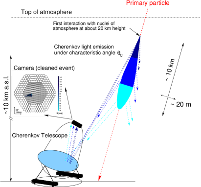
Since the details of the MAGIC telescope are described elsewhere [4], only items relevant to the FADC system are presented in this section. Figure 1 shows the working principle of an air Cherenkov telescope. A high energy gamma ray entering the earth’s atmosphere initiates a shower cascade of electrons and positrons. These radiate Cherenkov light, which is collected by the mirror and focussed onto the PMT camera of the MAGIC telescope. The main background originates from much more frequent showers induced by isotropic hadronic cosmic rays.
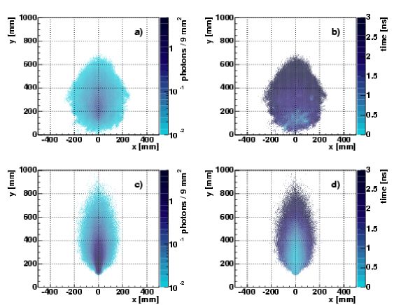
Monte Carlo (MC) based simulations predict different time structures for gamma and hadron induced shower images as well as for images of single muons. The timing information is therefore expected to improve the separation of gamma events from the background events [6]. Figure 2 shows the mean amplitude (a, c) and time (b, d) profiles for gamma (c, d) and hadron (a, b) induced air showers images on the camera plane of the MAGIC telescope. The impact parameter is fixed to 120 m and the initial gamma energy is set to 100 GeV, while the proton energy is set to 200 GeV. The profiles are obtained by averaging over many simulated showers [7]. Although the total shower duration of gamma and hadron induced air showers is comparable, the photon arrival time varies smoothly over the gamma shower image while hadron shower images are structured in time. The time structure of the image can also provide essential information about head and tail of the shower.
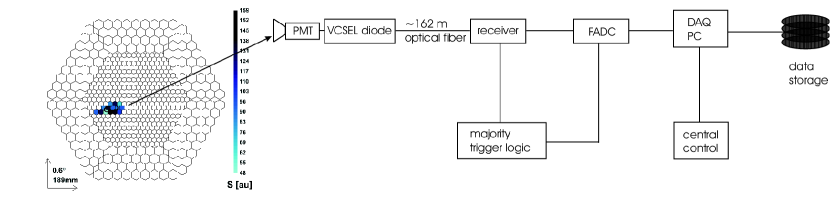
The MAGIC read-out chain, including the PMT camera, the analog-optical link, the majority trigger logic and FADCs, is schematically shown in figure 3. The response of the PMTs to sub-ns input light shows a pulse of FWHM of 1.0 - 1.2 ns and rise and fall times of 600 and 700 ps correspondingly [8]. By modulating vertical cavity surface emitting laser (VCSEL) diodes in amplitude the ultra-fast analogue signals from the PMTs are transferred via 162m long, multimode graded index 50/125 m diameter optical fibers to the counting house [9]. After transforming the light back to an electrical signal, the original PMT pulse has a FWHM of about 2.2 ns and rise and fall times of about 1ns.
In order to sample this pulse shape with the present 300 MSamples/s FADC system, the pulse is stretched to a FWHM of ns (the original pulse is folded with a stretching function of about 6ns). This implies a longer integration of LONS and thus the performance of the telescope on the analysis level is degraded.
Because the current MAGIC FADCs have a resolution of 8 bit only, the signals are split into two branches with a factor of 10 difference in gain. One branch is delayed by 55 ns and then both branches are multiplexed and consecutively read out by one FADC. The FADC system can be read out with a maximum sustained rate of 1 kHz. A 512 kbytes FIFO memory allows short-time trigger rates of up to 50 kHz.
3 The Ultra-fast Fiber-Optic MUX-FADC Data Acquisition System
The MAGIC collaboration is going to improve the performance of its telescope by installing a fast ( GSamples/s) FADC system, which fully exploits the intrinsic time structures of the Cherenkov light pulses. The requirements for such a system are the following:
-
•
10 bit resolution at a 2 GSamples/s sampling rate
-
•
MHz bandwidth of the electronics chain including the FADC
-
•
up to 1 kHz sustained event trigger rate
-
•
dead time .
3.1 General MUX-Principle
It is interesting to note that in experiments where FADCs are used to read out a multichannel detector in the common event trigger mode, only a tiny fraction of the FADC memory depth is occupied by the signal while the rest is effectively “empty” [11, 12]. One can try to correct this “inefficiency of use” by “packing” the signals of many channels sequentially in time into a single FADC channel, i.e. by multiplexing.
Following this simple idea, a multiplexing system with fiber-optic delays has been developed for the MAGIC telescope. The block diagram is shown in figure 4. The ultrafast fiber-optic multiplexer consists of three main components:
-
•
fiber-optic delays and splitters
-
•
multiplexer electronics: fast switches and controllers
-
•
ultra-fast FADCs.
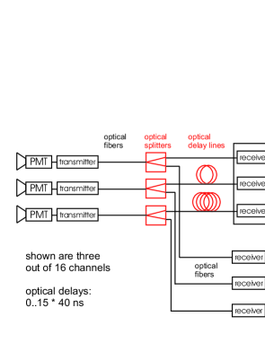
After the analog optical link between the MAGIC PMT camera and the counting house the optical signals are split into two parts. One part of the split signal is used as an input to the trigger logic. The other part is used for FADC measurements after passing through a fiber-optic delay line of a channel-specific length.
The multiplexer electronics operates in the following way: The common trigger from the majority logic unit opens the switch of the first channel and allows the analog signal to pass through and be digitized by the FADC. All the other switches are closed during this time. When the digitization window for the first channel is over the corresponding switch is closed. The closed switch strongly attenuates the signal transmission by more than 60 dB for the fast MAGIC signals. Then the switch number two is opened such that the accordingly delayed analog signal from the second channel is digitized and so forth, one channel at a time until the last one is measured. In this way one “packs” signals from different channels in a time sequence which can be digitized by a single FADC channel.
Because of the finite rise and fall times of the gate signals for the switches and because of some pick-up noise from the switch one has to allow for some switching time between the digitization of two consecutive channels. The gating time for each channel was set to 40 ns, of which the first and last 5 ns are affected by the switching process.
For the use in MAGIC a multiplexing ratio was chosen. 16 channels are read out by a single ultra-fast FADC channel. The chosen multiplexing ratio is a compromise between
-
•
Dead time: the digitization of one event takes 16*40 ns=640 ns. During this time no other event can be recorded. Compared to the maximum sustained trigger rate of up to 1 kHz this dead time is negligible.
-
•
Noise due to cross-talk through the closed switches: The attenuated noise of the other channels could influence the active signal channel.
-
•
Cost of the FADCs
-
•
Mechanical constraints, e.g. board size, length of wires and fibers.
3.2 Optical Delays and Splitters
Optical fibers were chosen for the analog signal transmission between the PMT camera and the counting house because they are lightweight, compact, immune to electro-magnetic pick-up noise and provide no pulse dispersion and attenuation [9]. The signal attenuation at 1 km fiber length is about 2.3 dB for the chosen 850 nm wavelength of the VCSELs. The analog signal transmission offers a dynamic range larger than 60 dB.
Using fiber-optic delays ultra-fast analog signals can be delayed by several hundreds of ns. Thus a large number of successively delayed signals can be multiplexed and read out by a single channel FADC. Part of the analog signal has to be split off before the delay lines for trigger. Therefore fiber-optic splitters of type are used.
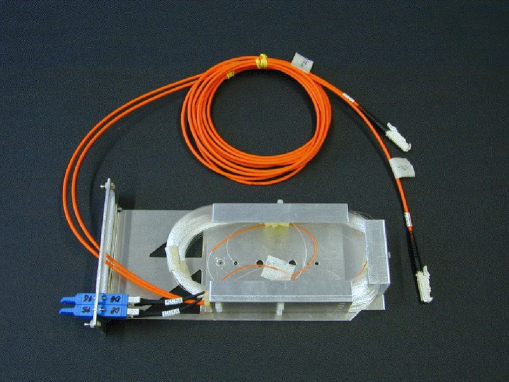
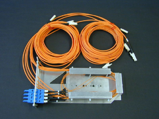
Figure 5 shows a module containing two optical delay lines of 142 m and 150 m length, corresponding to a delay of 710 ns and 750 ns. Figure 6 shows a module of four graded index (GRIN)-type fiber-optic splitters with 50:50 splitting ratio (for a technical description see [13]). The modules have standardized outer dimensions and can be assembled in 3U hight 19” crates. The splitters and optical delay lines are commercially available from the company Sachsenkabel [14].
3.3 MUX Electronics
The multiplexer electronics consist of four stages. The first stage is a fiber optic receiver, where the signals from the optical delay lines are converted back to electrical pulses using PIN diodes. In a second stage, part of the electrical signal is branched off and transferred to a monitor output. The third stage consists of ultra-fast switches which are activated one at a time. In the last stage all 16 channels are summed to one output. The multiplexed signals are then transferred via 50 coaxial cables to the FADC channels. Table 1 summarizes the specifications of the multiplexer electronics.
| Mechanical size | 370 mm (9 U) * 220 mm * 30 mm (6 HP) |
|---|---|
| Number of channels | 16 |
| Analog input | via 50/125 m graded index fiber, E2000 connector |
| Gain | 25, including the VCSEL transmitter |
| Dynamic range | max output amplitude: 1 V |
| Power supplies | +12 V, V |
| Power dissipation | 20 W |
| Trigger input | LVDS |
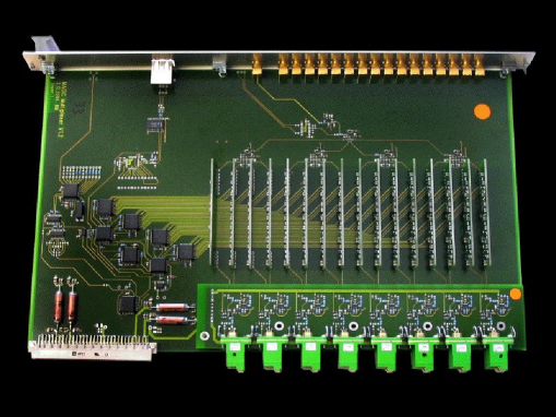
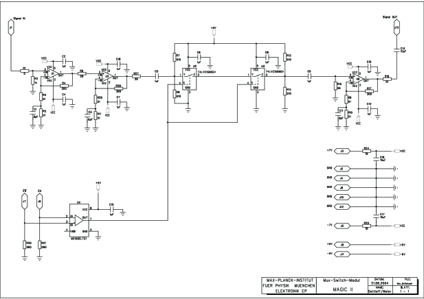
One multiplexer module consists of one 6 layer motherboard and 16 double layer switchboards, which are plugged into the motherboard via multiple pin connectors. Figure 7 shows a photo of the printed circuit MUX motherboard with 16 mounted daughter switchboards.
The motherboard includes the following components:
-
•
16 opto-electrical converters
-
•
16 monitor outputs
-
•
the Digital Switch Control circuit (DSC)
-
•
the trigger input to activate the DSC
-
•
16 ultra-fast switches on 16 switchboards
-
•
the 16 channel summing stage.
One opto-electrical converter consists of a receptacle, a PIN photo diode, packed in the E2000-connector. The photodiode is biased by 12 V to reduce its intrinsic capacity for speed and noise optimization. The current signal of the PIN photo diode is converted into an equivalent voltage signal by a transimpedance-amplifier. Its amplifier-IC has a gain-bandwidth product of about 1.5 GHz and a very high slew rate of about 4000 V/s. The trans-impedance is 1000 . A monitor output consists of an ultra-wide band (UWB)-driver-amplifier, which transmits the signal from the transimpedance-stage to a 50 -SMA-connector.

Figure 8 shows the circuit diagram of the Digital Switch Control circuit, DSC. It consists of the following parts:
-
•
One clock generator-IC. It is programmable with a resolution of 12 bit from 50 MHz to 800 MHz and works in PECL mode. It is crystal stabilized and set to 800 MHz.
-
•
A digital delay line (DDL) that can be set from 2 ns to 10 ns with 11 bit accuracy. It can be used to adjust the trigger times between different MUX motherboards.
-
•
A digital lock-in-circuit (DLC) synchronizes the MUX-sequence to the trigger signal. The lock-in jitter is 1.25 ns ().
-
•
16 differential PECL-drivers that transmit the MUX-sequence signals to the corresponding switchboards.
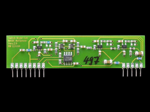
Each switchboard includes two ultra-wideband (UWB)-amplifier circuits, followed by two ns-switching MOSFETs operated in series and one UWB-driver-amplifier-circuit. MOSFET switches were chosen due to their fast switching properties and a very fast stabilization of the signal baseline after the switching. The small cross-talk through the closed switch is further reduced by the serial operation of two switches. An on-board PECL to CMOS converter distributes the digital switch-control-circuit (DSC)-signal to the MOSFET-switches in parallel. Figure 9 shows a photo of the switch board, while its circuit diagram is shown in figure 10.
In a passive summation, the switch parasitic capacitances would add up and can significantly widen the signal pulse. To avoid this, a two-step active summation was chosen: In the first step, the outputs of four channels are summed together. In the second step, the four resulting outputs are summed into one. For the summing UWB-amplifiers are used. The two-step setup keeps the channel wires short, and permits to use the amplifiers in the faster inverting mode while keeping the signal polarity non-inverting. Finally, an UWB-driver sends the multiplexed signals over a 50 -SMA-coaxial connection to the FADC. The circuit diagram of the summation stage is shown in figure 11.

3.4 FADC Read-Out
The FADCs are commercial products manufactured by the company Acqiris (DC 282) [15]. They feature a 10 bit amplitude resolution, a bandwidth of 700 MHz, a sampling speed of 2 GSamples/s and an input voltage range of 1 V. Each FADC board contains 4 channels. The read-out data are stored in a RAM on the FADC board of 256 kSamples (512 kbytes) size per channel. Up to 4 FADC boards can be arranged in one compact PCI crate and are read out by a crate controller PC running under Linux. The FADCs are designed for a 66 MHz 64 bit data transfer via the compact PCI bus.
The FADC features a trigger time interpolator TDC that can be used to correct for a potential trigger jitter of 500 ps due to the asynchronous FADC clock with respect to the trigger decision. Table 2 summarizes the specifications of the ultra-fast FADCs.
| Mechanical size | 267 mm (6 U) * 220 mm * 30 mm (6 HP) |
|---|---|
| Number of channels | 4 |
| Analog input | 1 V full scale, adjustable offset |
| Sampling frequency | 2 GSamples/s |
| Sampling resolution | 10 bits |
| RAM size | 256 kSamples (512 kbytes) per channel |
| Bandwidth | 700 MHz |
| Noise level | LSB guaranteed |
| Power dissipation | 60 W (4 channels) |
| Trigger input | unipolar, adjustable threshold |
4 Performance of the System Components
The performance of the MUX-FADC system components was studied in extensive laboratory tests. The quality and performance of the FADCs and of different commercially available optical splitters and delays were evaluated. Several iterations of the multiplexer electronics design were made.
4.1 Performance of the Optical Delays and Splitters
The fiber-optic delay lines have channel-specific delay times of 0…15 times 40 ns plus 500 ns common base delay. Deviations from the specified delay times and potential changes in the delay due to temperature variations are important. It has to be ensured that all signals arrive in time at the multiplexer electronics when a given switch is open.
The manufacturer guarantees for the delay length a maximum deviation of 2 ns from its nominal value. This was confirmed in laboratory measurements. Although the signal attenuation in fibers is small, nevertheless, there are small differences in the dispersion of the signals in different channels due to the different delay lengths.
Different technologies of fiber-optic splitters are available on the market. Three splitting technologies were tested: fused splitters, bifurcation splitters and so called GRIN-splitters. In the fused technology two optical fibers are drilled and then thermally fused together. In bifurcation splitters the end faces of the two output fibers are mechanically attached to the end face of the input fiber. In GRIN-type splitters the splitting is done by a semi-transparent mirror in conjunction with two graded index lenses [13].
The MAGIC optical link uses multimode VCSELs and multimode optical fibers. Mechanical stress or deformations of the input fiber into the splitter, especially due to telescope movements, can vary the propagation of light modes in the fiber. The expected movements of the fibers were simulated in the laboratory by bending the fibers using different bending radii. The fused and bifurcation fiber-optic splitters show changes in the splitting ratio of more than 10 %. Only the so called GRIN type splitters are immune against mode changes, with measured changes of the splitting ratio of less than 1%.
The splitting ratio is guaranteed to be 50:50 within % by the manufacturer. This was again confirmed in test measurements. All tested splitters were found to be insensitive with respect to time and temperature changes.
4.2 Performance of the MUX Electronics
The MUX electronics was extensively tested in the laboratory. For the use as a read-out system for MAGIC, the following points are very important:
-
•
short switching noise and flat signal base-line
-
•
high bandwidth (low pulse dispersion in amplitude and in time)
-
•
strong signal attenuation for closed switches
-
•
good linearity and large dynamic range
-
•
stability.
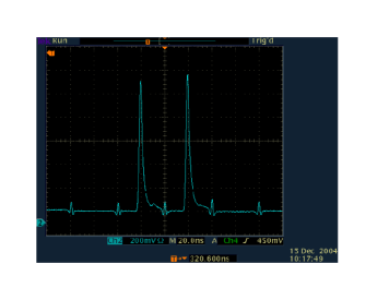
Figure 12 shows a photo recorded with a fast oscilloscope of two consecutively multiplexed signals along with the switching noise between two channels. Although the switching noise is as large as 100 mV, it is very reproducible and confined to less than 10 ns of the 40 ns window per read-out channel. In the rest of the window the baseline is flat and stable.
The switching and summing stages only slightly widen the fast input pulses. A pulse of about 2.5 ns FWHM after the receiver photo diode is widened to 2.7 ns FWHM at the output of the multiplexer electronics. The pass-through of such fast signals through closed switches is less than 0.1% (60 dB attenuation).
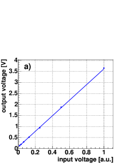
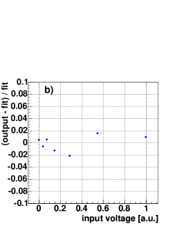
Figure 13a shows the combined linearity of the switches and of the summing stage. The output signal amplitude of the MUX-board is plotted as a function of the input signal amplitude after the PIN-Diode, as measured at the monitor output. The right panel of the figure shows the deviations from linearity of the MUX-electronics. For output signals up to 1 V the MUX- electronics is linear with differential deviations less than 2%. The total non-linearity of the read-out chain is dominated by the analog optical link. Its response deviates from a perfect linear behavior by less than 10% in a total range of 56 dB [10].
4.3 FADC Performance
The main performance parameters of the FADC are
-
•
noise level / effective dynamic range
-
•
linearity and bandwidth
-
•
maximum trigger and acquisition rate
-
•
dead time.
A noise level of less than 1.2 least significant bits (LSBs) is guaranteed by the manufacturer (700 MHz bandwidth, no input amplifier). There are small but constant differences in the input voltage full scales and thus in the gain for different FADC channels. These can be corrected for by the offline calibration software. The FADCs feature an internal calibration system keeping their integral and differential non-linearity below one LSB.
For the maximum trigger rate and the dead time optimization the interplay between the FADC boards and the crate controller PC is important. The compact PCI (cPCI) bus allows an effective data throughput of up to about 400 Mbytes/s (66 MHz, 64 bit) shared between all FADC channels in one crate.
In each event 2560 bytes are stored per FADC channel (16 channels of 40 ns gate time, 2 GSamples/s and 2 bytes per sample for the 10-bit resolution FADC). Reading out 8 FADC channels with one crate controller board results in a data volume of about 20 kbytes/event, which has to be transferred via the cPCI bus.
The ultra-fast FADC offers three modes of data acquisition:
-
•
single acquisition
-
•
segmented memory
-
•
asynchronous acquisitions using a FIFO memory.
In the single acquisition mode the FADC writes the digitized data into the on-board RAM using it as one big ring buffer. Upon the arrival of a trigger the bytes corresponding to the event are copied to the PC with a DMA transfer via the cPCI bus. The read-out time per event and per FADC channel in the crate is given by the sum of the DMA overhead time, s and the data transfer time over the cPCI bus [15]:
| (1) |
is the data throughput of the cPCI bus for the 64 bit, 66 MHz operation.
For 8 FADC channels per crate this amounts to a total transfer time of about s. Including a s global trigger rearm time this leads to about s dead time per event.
In the segmented mode the FADC RAM is divided into many segments. Each segment is used as a circular buffer where the digitized data is stored. After the arrival of a trigger the digitizer continues to write into the next segment. The dead time between two events is s. When all segments are filled the data is copied to the PC via one DMA transfer. The total readout time for M segments is:
| (2) |
where denotes the number of “overhead” data points per segment.
In the current scheme an additional time to reorder the data inside the PC has to be taken into account. For 8 FADC channels in one crate and 100 segments the total dead time amounts to ms, i.e. s per event.
The most attractive operation mode uses the FADC RAM as a FIFO. In this case the FADC writes the digitized data in one part of the RAM while previously stored data is asynchronously transfered to the PC. The dead time is thus reduced to the s needed to rearm the trigger. Additional dead time arises only if the average trigger rate exceeds the maximum sustainable rate of 2 kHz.
5 Prototype Test in the MAGIC Telescope on La Palma
Two prototype MUX-FADC read-out modules for 32 channels were tested as a read-out of the MAGIC telescope during two weeks in August/September 2004.
The main goals for the tests were:
-
•
test of concept of the ultra-fast MUX-FADCs under realistic conditions
-
•
study the interplay of the MUX-FADC system with the MAGIC trigger and data acquisition system
-
•
implement the reconstruction and calibration for the ultra-fast digitized signals in the common MAGIC software framework MARS [16]
-
•
provide input for detailed MC simulations for the ultra-fast digitization.
5.1 Setup of the Prototype Test
Two MUX boards of 16 channels each were integrated into the MAGIC read-out system allowing the simultaneous data taking with the current 300 MSamples/s read-out and the MUX-FADC prototype read-out. Figure 14 shows in a block diagram how the MUX-FADC prototype read-out system was integrated into the current MAGIC FADC read-out. The analog optical signals arriving from the MAGIC PMT camera were split into two equal parts using fiber-optic splitters. One part of the optical signal was connected to the current MAGIC receiver boards which provided output signals to the MAGIC majority trigger logic [17] and to the current 300 MSamples/s FADCs. The other part of the optical signal was delayed by a channel specific delay of 0…15 times 40 ns plus common base delay and directed to the optical receivers on the MUX boards. The common MAGIC trigger was used to trigger the MUX boards as well as the fast FADCs.
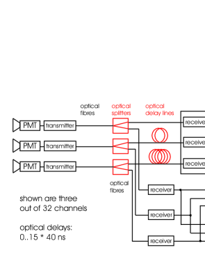
Figure 20 shows the group of 32 selected channels of the MAGIC PMT camera [4] to be read out by the ultra-fast digitizing system. The channels were chosen to be close packed in order to contain (at least partially) images of showers. In the test 16 bifurcation and 16 GRIN type splitters were used.
In order to acquire only events where the shower image is located in the 32 MUX-FADC channels, only these channels were enabled in the MAGIC trigger system. The trigger fires if the signal in at least four close packed pixels exceeds the preset threshold.
In the prototype tests on La Palma an older version of the ultra-fast FADC was used, the Acqiris DC 240. It features a sampling speed of 2 GSamples/s with an 8 bit resolution. It was connected via a PCI bridge to a host PC running under Windows.
For every trigger 1300 FADC samples (16 times 80 samples plus 20 extra samples) were recorded with both of the used multiplexed FADC channels. An FADC memory of 120 segments was used. In the host PC the data were written into a binary file. This setup was chosen for simplicity and was not optimized for the smallest dead time in a continuous data taking mode. Nevertheless, the dead time between two of the 120 consecutively recorded events in the segmented mode was negligible.
5.2 The Data
The tests of the MUX-FADC system were carried out around the full moon period. In total about 230000 triggers were taken with the MUX-FADC read-out system (including pedestals and calibration LED light pulses). Table 3 summarizes the amount of data taken with and without the presence of moon light.
| trigger type | current FADC read-out | MUX-FADC read-out |
|---|---|---|
| pedestals, no moon | 500 | 26400 |
| pedestals, moon | 5000 | 13210 |
| calibration, no moon | 47000 | 96000 |
| calibration, moon | 91000 | 70420 |
| cosmics, no moon | 500 | 8040 |
| cosmics, moon | 0 | 16800 |
| total | 144000 | 230870 |
5.3 Data analysis
Each data file contains 120 events of two ultra-fast FADC channels with 1300 recorded FADC samples per event. The recorded raw data are converted into the usual ROOT-based MAGIC raw data format [16], which provides the flexibility to adjust the number of recorded samples for each pixel.
5.3.1 Signal Reconstruction
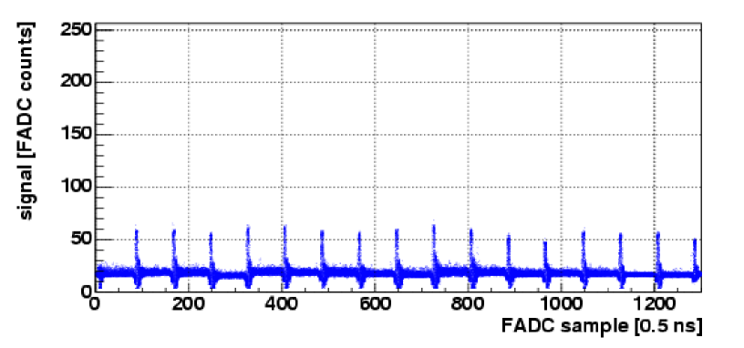
For each event the signals of 16 PMTs of the MAGIC camera are sequentially digitized by one FADC channel. As an example, figure 15 shows the raw data for 120 superimposed randomly triggered pedestal events. Between every two consecutive channels the switch noise is visible.
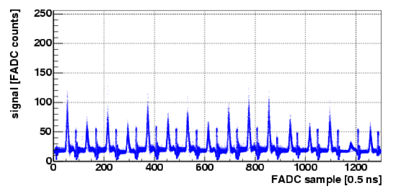
For calibration purposes the MAGIC PMT camera can be uniformly illuminated by a fast LED light pulser located in the center of the telescope dish [18]. Figure 16 shows the raw data of 16 consecutively read-out channels for 120 superimposed calibration events. The calibration signal pulses are clearly visible on the signal baseline. The gain difference from channel to channel is mainly due to a spread in the gain of the VCSEL and receiver diodes of the analog optical link. The additional spread due to small differences in the fiber-optic splitters and a signal attenuation in the delay lines is small.
For each channel the pedestal level and pedestal RMS are calculated from either a pedestal run with random triggers or directly from the data. For the pedestal calculation a fixed number of FADC samples at a fixed position in the digitization window is used.
For the signal reconstruction a fixed number of FADC samples is integrated. The integration interval was chosen to be 4 FADC samples (corresponding to 4*3.33 ns = 13.33 ns) for the current MAGIC FADCs. For the MUX-FADCs a window size of 10 FADC samples is chosen, corresponding to a 5 ns integration window. The reconstructed signal is then given by:
| (3) |
where is the i-th FADC sample after the trigger. The signal arrival time relative to the first FADC sample after the trigger, , is reconstructed as the first moment of the FADC time samples used to calculate the reconstructed signal:
| (4) |
5.3.2 Calibration
The calibration system of the MAGIC telescope consists of intensity controlled fast LED light pulsers of different colors and intensities that illuminate the MAGIC camera homogeneously [18]. Using the laboratory measured excess noise factor of the MAGIC PMTs the conversion constant between reconstructed signals in FADC counts and photo electrons can be determined. The common MAGIC calibration algorithms and software were successfully applied to the ultra-fast digitization.
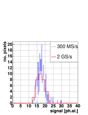
Figure 17 shows the distribution of the mean number of photo electrons per pixel reconstructed with the current 300 MSamples/s FADC system and the MUX-FADC system. The MAGIC camera was illuminated with UV calibration pulses of about 2.5 ns FWHM. As expected, the mean reconstructed number of photo electrons is the same for the 32 split channels used in the MUX-FADC tests as for all the other MAGIC read-out channels.
Small differences in the cable length of the MAGIC analog optical link, the fiber-optic delays and transition times in the PMTs introduce arrival time differences between of the pulses in different read-out channels of up to a few ns. These relative channel to channel time differences can also be calibrated using the LED pulser. One can determine the mean time difference between all pixels with respect to a reference pixel. In the calibration procedure of the cosmics events this timing difference is corrected for.
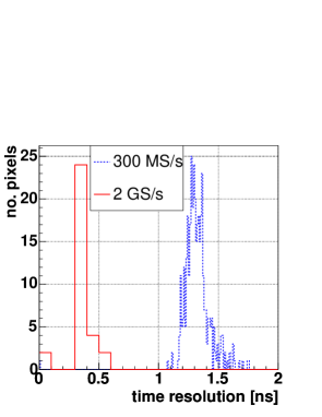
In addition, the event to event variation of the timing difference between two read-out channels for the LED pulser provides a measure of the timing accuracy. Figure 18 shows the distributions of the determined timing resolution of the current 300 MSamples/s FADCs together with the timing resolution of the MUX-FADCs. The timing accuracy strongly depends on the signal to noise ratio and the width of the input light pulse. The MUX-FADCs yield a better timing resolution by more than a factor of three compared to the current FADC system using the simple and stable timing extraction algorithm of equation (4).
5.3.3 Cosmics Data
Cosmics shower data were recorded to study in detail the interplay of the ultra-fast MUX-FADC system with the MAGIC trigger logic. It also provides valuable input for the MAGIC MC simulations of the ultra-fast digitization system, e.g. about the pulse shapes for cosmics events.
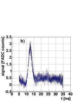
In figure 19a one can see the pulse shape in a single pixel for a typical cosmics event. By overlaying the recorded FADC samples of many events after adjusting to the same arrival time, the average reconstructed pulse shapes can be calculated. Figure 19b shows the comparison of the average reconstructed pulse shapes recorded with the current 300 MSamples/s MAGIC FADCs, including the 6ns pulse stretching, and with the MUX-FADCs. The average reconstructed pulse shape for cosmics events has a FWHM of about 6.3 ns for the current FADC system and a FWHM of about 3.2 ns for the MUX-FADC system.
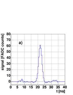
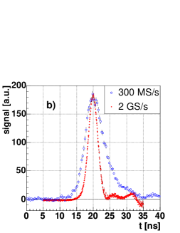
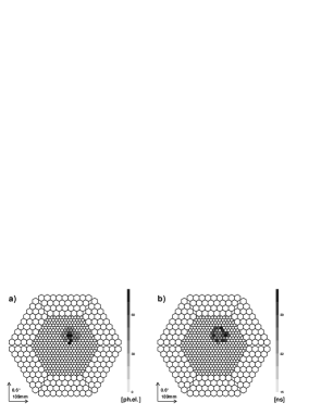
Figure 20a shows a MAGIC PMT camera display with the reconstructed signal after calibration in photo electrons for a typical cosmics event. For the same event figure 20b shows the reconstructed arrival time after correction for the cannel-to-channel time differences.
5.3.4 Pedestals / Noise
In the data recorded by an IACT, the electronics noise together with the LONS fluctuations is superimposed on the Cherenkov signal from air-showers. The noise from the LONS can be simulated as the superposition of the detector response to single photo electrons, arriving at a given rate but randomly distributed in time. This can be quantified using the noise autocorrelation function , the correlation between the read-out samples and :
| (5) |
where and are the FADC samples and for a pedestal event.
Figure 21 shows the noise autocorrelation for the current MAGIC FADC system and the MUX-FADC system with open camera (i.e. exposed to LONS), normalized to the pedestal RMS. In the same plot, the noise autocorrelation for the MUX-FADC system with closed camera (no LONS), normalized to the pedestal RMS for an open camera, is shown. The noise autocorrelation of the current FADC system extends to several ns since the pulse is stretched by 6 ns. For the MUX-FADC system with no pulse shaping there is still a considerable noise autocorrelation for an open camera. The noise autocorrelation mostly disappears in case of a closed camera with electronics noise only.
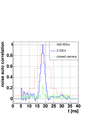
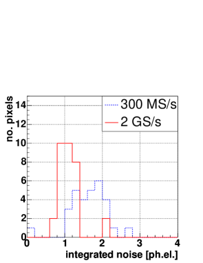
Figure 22 shows the distributions of the integrated noise (integrated pedestal RMS after calibration in photo electrons) per pixel for the current FADC system and for the MUX-FADC system. The shorter integration time used for the pulse reconstruction with the MUX-FADC system yields a reduction of the effective integrated noise by about 40%.
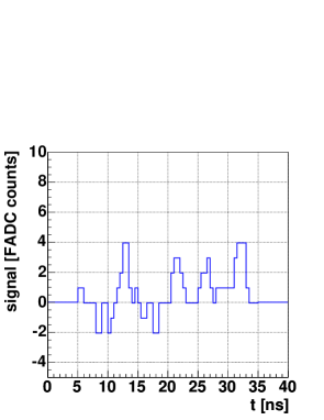
Using the new MUX-FADC system the noise contributions due to the LONS may even be resolved into individual pulses. Figure 23 shows a typical example for the signals in a pedestal event (random triggers). The pedestal does not vary in an uncorrelated way. Instead most of the pedestal variations are due to peaks on the signal baseline.
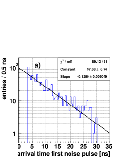
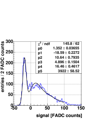
The rate of the peaks was studied to verify whether it is compatible with the rate of LONS photo electrons. A window of 6 slices is slid over the FADC samples of randomly triggered pedestal events. The first window position after the switch noise where the sum of the FADC samples exceeds the pedestal level by at least 3 FADC counts was chosen. Figure 24a shows the arrival time distribution of the first noise peak. The distribution can be fit by an exponential function with a rate of
| (6) |
This corresponds to an integrated LONS charge of about 1.3 photo electrons per 10 ns integration window, which is in good agreement with the expected LONS rate.
Figure 24b shows the pulse shape of the selected noise peak averaged over many events. It has a FWHM of about 2.6 ns. This corresponds to the response of the instrument to a -function input pulse (single LONS photo electrons have no internal time structure). The mean charge of the noise peak corresponds within errors to the mean charge for a single photo electron.
The 8 bit amplitude resolution in the test setup was somewhat limiting the resolution of the single photo electrons due to the LONS. With the higher resolution of 10 bit with the full MUX-FADC system even a continuous calibration of the read-out chains using the single photo electrons shall be possible.
5.3.5 MC Simulations
The response of the MAGIC telescope to gamma ray showers and to background was simulated in detail [19]. Both the currently used 300 MSamples/s readout chain and the ultra-fast digitization were simulated.
Figure 25 shows the reconstructed single photo electron spectrum of a simulated pedestal run. The highest integral of 8 FADC slices (4 ns) was searched for in a fixed digitization window of 20 slices (10 ns). The leftmost peak corresponds to electronics noise only. The right part of the distribution corresponds to the response of the PMT to one or more photo electrons.
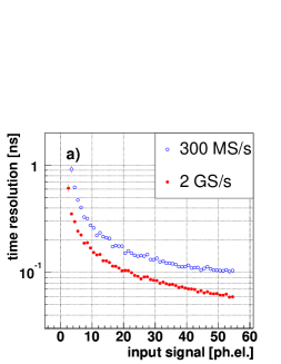
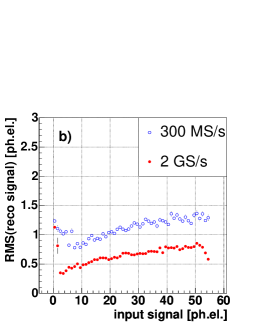
In figures 26 the signal and arrival time resolutions of the current and the MUX-FADC system are compared using MC simulations. For both MC simulations the same LONS conditions are assumed as well as the same electronics noise level. In the simulation no intrinsic transit time spread of the PMTs of about 250 ps per photo electron was taken into account. The input light pulse has a FWHM of 1 ns as expected for gamma-ray induced showers.
Contrary to the simple signal and arrival time extraction algorithms used above, a dedicated numerical fit to the FADC samples using a known pulse shape [20, 21] has been applied to illustrate the theoretically achievable resolution. Figure 26a shows the resolution of the reconstructed pulse arrival time as a function of the input signal. The MUX-FADC system improves the timing resolution by nearly a factor of 2. Figure 26b shows the resolution of the reconstructed charge as a function of the input charge. With the MUX-FADC system the charge resolution improves by a factor of two.
6 Discussion
The ultra-fast fiber-optic multiplexed FADC prototype read-out system was successfully tested during normal observations of the MAGIC telescope in La Palma. The fiber-optic splitters and delays are commercially available and comply with the required specifications for the use in the ultra-fast MUX-FADC read-out system. The 10 bit 2 GSamples/s FADCs from Acqiris have been developed for MAGIC, and are available now as a commercial product. Thus the ultra-fast FADC read-out has grown to a mature technology which is ready for the use as a standard read-out system for the MAGIC telescope and other high-speed data acquisition applications.
The multiplexing of 16 channels into one ultra-fast FADC allows one to greatly reduce the price of an ultra-fast read-out system. The MUX-FADC read-out reduces the costs by about 85% compared to using one ultra-fast FADC per read-out channel. Also the power consumption of the read-out system is greatly reduced.
The ultra-fast MUX-FADC system allows to skip the artificial pulse stretching and thus to use a shorter integration window for the Cherenkov pulses. The reduction of the pulse integration window from 13.33 ns (4 samples with 3.33 ns per sample) for the current MAGIC FADC system to 5 ns (10 samples with 0.5 ns per sample) for the MUX-FADC system corresponds to a reduction of the integrated LONS charge by a factor of about 2.7. Consequently, the RMS noise of the LONS is reduced by about 40%.
The recorded images of the air showers are usually, at least for energies above 100 GeV, characterized by so-called Hillas parameters [22]. In order to prepare raw shower images for the Hillas parameter calculation it is necessary to apply so-called tail cuts to reject pixels with a low signal to noise ratio. All pixels with signals below 3 times their noise RMS (mainly due to LONS) are rejected (dynamic image tail cut cleaning).
A reduction in the noise RMS translates into lower image cleaning levels. Thus a larger part of the shower image, or in other words a shower image of a higher signal to noise ratio, can be used to calculate Hillas parameters. This is especially important for low energy events where the signals of only a few pixels are above the image cleaning levels. The image quality of the air showers will improve with the ultra-fast read-out system. This will allow the reduction of the analysis energy threshold of the MAGIC telescope.
The ultra-fast FADC system also provides an improved resolution of the timing structure of the shower images. As indicated by MC simulations [6] gamma showers, cosmic ray showers and the so called single muon events have different timing structures. Thus the ultra-fast FADC read-out can enhance the separation power of gamma showers from backgrounds.
After the successful prototype test of the ultra-fast MUX-FADC read-out system it is ready to be installed as a future read-out of the MAGIC telescope.
Appendix A Acknowledgements
The authors thank R. Maier and T. Dettlaf from the electronics workshop of MPI for the layout, design and production of the MUX-FADC electronics. We also acknowledge the very good collaboration with the companies Acqiris and Sachsenkabel.
References
- [1] E. Lorenz, Very High Energy Gamma Ray Astronomy, Nucl.Phys.B (Proc.Suppl.) 114 (2003) 217.
- [2] J. A. Barrio (MAGIC Collab.), The MAGIC Telescope - Design Study for the Construction of a 17m Cherenkov Telescope for Gamma Astronomy above 10 GeV, MPI-PhE-98-05.
- [3] F. Goebel et al. (MAGIC Collab.), The data acquisition of the MAGIC telescope, in 28th International Cosmic Ray Conference Proceedings, Frontiers Science Series 41, Universal Academy Press Tokyo, 2003.
- [4] C. Baixeras et al. (MAGIC Collab.), Commissioning and first tests of the MAGIC telescope, Nucl. Instrum. Meth. A518 (2004) 188.
- [5] S. Commichau, private communication.
- [6] R. Mirzoyan et al., Muon rejection using timing in air Cherenkov telecopes, to be published in proceedings of the conference Towards a Network of Atmospheric Cherenkov Detectors VII, 27-29 April 2005 Palaiseau, France.
- [7] D. Mazin et al., Shower templates for the MAGIC Telescope, In preparation.
- [8] A. Ostankov et al., A study of the new hemispherical 6-dynodes PMT from electron tubes, Nucl. Instrum. Meth. A442 (2000) 117.
- [9] E. Lorenz et al., A fast, large dynamic range analog signal transfer system based on optical fibers, Nucl. Instrum. Meth. A461 (2001) 517.
- [10] D. Paneque et al. (MAGIC Collab.), Analogue signal transmission by an optical fiber system for the camera of the MAGIC telescope, in 28th International Cosmic Ray Conference Proceedings, Frontiers Science Series 41, Universal Academy Press Tokyo, 2003.
- [11] R. Mirzoyan et al., Ultrafast FADC Multiplexer, IEEE Trans. Nucl. Sci. 49 (2002) 2473 .
- [12] R. Mirzoyan, J. Cortina and E. Lorenz, Multiple Signal Channel Read Out by a Single FADC, in Proceedings of the 27th International Cosmic Ray Conference, Kopernicus Gesellschaft, 2001.
- [13] J. Lipson and G. Harvey, Low-loss wavelength division multiplexing (WDM) devices for single-mode systems, Journal of Lightwave Technology 1 (1983) 387.
- [14] Sachsenkabel GmbH, http://www.sachsenkabel.de.
- [15] Acqiris SA, http://www.acqiris.com.
- [16] T. Bretz and R. Wagner (MAGIC Collab.), The MAGIC analysis and reconstruction software, in 28th International Cosmic Ray Conference Proceedings, Frontiers Science Series 41, Universal Academy Press Tokyo, 2003.
- [17] M. Meucci et al. (MAGIC Collab.), The trigger system of the MAGIC telescope: On-line selection strategies for Cherenkov telescopes, Nucl. Instrum. Meth. A518 (2004) 554.
- [18] T. Schweizer et al., The optical calibration of the MAGIC telescope camera, IEEE Trans. Nucl. Sci. 49 (2002) 2497.
- [19] A. Moralejo et al., MC Simulations for the MAGIC Telescope, In preparation.
- [20] W. E. Cleland and E. G. Stern, Signal processing considerations for liquid ionization calorimeters in a high rate environment, Nucl. Instrum. Meth. A338 (1994) 467.
- [21] H. Bartko et al. (MAGIC Collab.), FADC Pulse Reconstruction Using a Digital Filter for the MAGIC Telescope, to be published in proceedings of the conference Towards a Network of Atmospheric Cherenkov Detectors VII, 27-29 April 2005 Palaiseau, France.
- [22] A. M. Hillas, Cherenkov light images of EAS produced by primary gamma, in 19th International Cosmic Ray Conference Proceedings, NASA, 1985.