SLAC–PUB–10393
March, 2004
Performance of a Low Noise Front-end ASIC for Si/CdTe Detectors
in Compton Gamma-ray Telescope
***Work supported by
Department of Energy contract DE–AC03–76SF00515, Grantin-Aid by Ministry of Education, Culture, Sports, Science and Technology of Japan (12554006, 13304014),
and “Ground-based Research Announcement for Space Utilization” promoted by Japan Space Forum.
Hiroyasu Tajima1, Tatsuya Nakamoto2, Takaaki Tanaka3,4, Shingo Uno2, Takefumi Mitani3,4, Eduardo do Couto e Silva1, Yasushi Fukazawa2, Tuneyoshi Kamae1, Grzegorz Madejski1, Daniel Marlow,5 Kazuhiro Nakazawa3, Masaharu Nomachi,6 Yu Okada4 and Tadayuki Takahashi3,4
1Stanford Linear Accelerator Center, Stanford University, Stanford, CA 94309
2Department of Physics, Hiroshima University, Higashi-Hiroshima 739-8526, Japan
3Institute of Space and Astronautical Science, Sagamihara, Kanagawa 229-8510, Japan
4Department of Physics, University of Tokyo, Bunkyo-ku, Tokyo 113-0033, Japan
5Department of Physics, Priceton University, Princeton, NJ 08544
6Department of Physics, Osaka University, Toyonaka, Osaka 560-0043, Japan
Abstract
Compton telescopes based on semiconductor technologies are being developed to explore the gamma-ray universe in an energy band 0.1–20 MeV, which is not well covered by the present or near-future gamma-ray telescopes. The key feature of such Compton telescopes is the high energy resolution that is crucial for high angular resolution and high background rejection capability. The energy resolution around 1 keV is required to approach physical limit of the angular resolution due to Doppler broadening. We have developed a low noise front-end ASIC (Application-Specific Integrated Circuit), VA32TA, to realize this goal for the readout of Double-sided Silicon Strip Detector (DSSD) and Cadmium Telluride (CdTe) pixel detector which are essential elements of the semiconductor Compton telescope. We report on the design and test results of the VA32TA. We have reached an energy resolution of 1.3 keV (FWHM) for 60 keV and 122 keV at 0∘C with a DSSD and 1.7 keV (FWHM) with a CdTe detector.
Index terms – Analog integrated circuits, Gamma-ray detectors, Compton Camera, Silicon radiation detectors, Cadmium Telluride.
Contributed to
IEEE Nuclear Science Symposium
Portland, Oregon USA
October 19–October 25, 2003
I Introduction
The gamma-ray universe in the energy band above 0.1 MeV provides a rich ground to study nucleosynthesis and physics of particle acceleration beyond thermal emission. However, the energy band between 0.1 MeV and 100 MeV is poorly explored due to difficulties associated with the detection of such photons. The Compton telescope COMPTEL [1] on board CGRO (Compton Gamma-Ray Observatory) demonstrated that a gamma-ray instrument based on the Compton scattering is useful for the detection of the gamma-ray in this energy band. COMPTEL provided us rich information on a variety of gamma-ray emitting objects either in continuum and line emission. The continuum sources include spin-down pulsars, stellar black-hole candidates, supernovae remnants, interstellar clouds, active galactic nuclei (AGN), gamma-ray bursts (GRB) and solar flares. Detection has also been made of the nuclear gamma-ray lines from 26Al (1.809 MeV), 44Ti (1.157 MeV), and 56Co (0.847 and 1.238 MeV).
Although COMPTEL performed very well as the first Compton telescope in space for MeV gamma-ray astrophysics, it suffered severely from large background, poor angular resolution, and complicated image decoding [2]. In 1987, T. Kamae et al. proposed a new Compton telescope based on a stack of silicon strip detectors (SSD) [3, 4]. This technology presents very attractive possibilities to overcome the weaknesses of COMPTEL as described later in this document. This idea of using silicon strip detectors stimulated new proposals for the next generation Compton telescope [5, 6, 7, 8].
Recently, a new semiconductor detector based on Cadmium Telluride (CdTe) emerged as a promising detector technology for detection of MeV gamma-rays [9, 10]. Taking advantage of significant development in CdTe technology, we are developing a new generation of Compton telescopes, the SGD (Soft Gamma-ray Detector) [6] onboard the NeXT (New X-ray Telescope) mission proposed at ISAS (Institute of Space and Astronautical Science) as a successor of the Astro-E2, and the SMCT (Semiconductor Multiple-Compton Telescope). The NeXT/SGD is a hybrid semiconductor gamma-ray detector which consists of silicon and CdTe detectors to measure photons in a wide energy band (0.05–1 MeV); the silicon layers are required to improve the performance at a lower energy band (0.3 MeV). The NeXT/SGD is a Compton telescope with narrow field of view (FOV), which utilizes Compton kinematics to enhance its background rejection capabilities. The SMCT will have a wider energy band (0.1–20 MeV) and a wide field of view (60∘). Excellent energy resolution is the key feature of the NeXT/SGD and SMCT, allowing to achieve both high angular resolution and good background rejection capability. It is worthwhile mentioning an additional capability of the NeXT/SGD and SMCT, their ability to measure -ray polarization, which opens up a new window to study properties of astronomical objects.
A low noise front-end ASIC is a fundamental element of semiconductor Compton telescopes. In this paper, we report on the design of the front-end ASIC and test results of prototype systems.
II Multiple-Compton technique
A stack of many thin scatterers is used in the multiple-Compton technique [3], which can accommodate more elements in the stack, thereby increasing the detection efficiency while maintaining the ability to record individual Compton scatterings. Fig. 1 illustrates the case for two Compton scatterings and one photoelectric absorption. In this situation, the scattering angles and can both be obtained from the recoil electron energies from the relations
| (1) | |||||
| (2) |
where , and are the energy deposited in each photon interaction. Note that can be also reconstructed from the hit positions of the three interactions. The order of the interaction sequences, hence the correct energy and direction of the incident photon, can be reconstructed by examination of this constraint for all possible sequences. This over-constraint also provides stringent suppression of random coincidence backgrounds. The direction of the incident photon can be confined to be on the surface of a cone determined from and the first two interaction positions. Precise energy resolution†††Here, energy resolution includes all sources such as noise, gain uncertainty and fluctuation of electron-hole pair generation in the detector. The noise is the dominant source in our application. for the recoil electron is the critical feature in the design of Compton telescope since the angular resolution of the incident photon, and the background rejection capability are determined by the Compton kinematics. We have demonstrated that the Compton technique can be used to measure the photon direction and polarization using a stack of SSD and CdTe detectors as described in [11, 12].
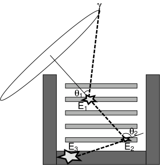
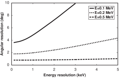
Fig. 2 shows the angular resolution as a function of the energy resolution for photons scattering in silicon with incident energies of 100, 200 and 500 keV at where is the polar angle of the Compton scattering. Due to Doppler braodening effect, the energy resolution below 1 keV does not necessarily result in better angular resolution for the incident photon energy above 100 keV. In order to achieve the energy resolution of 1.0 keV (FWHM, Full-Width at Half Maximum) for the silicon, a low noise ASIC with an equivalent noise charge (ENC) of better than 120 (rms) is required.
 |
III Low Noise ASIC
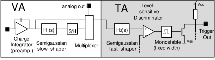
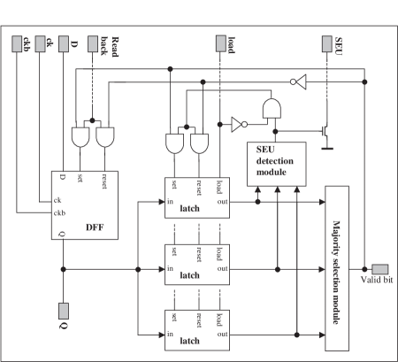
We have developed the VA32TA front-end ASIC based on the design of the VA32C amplifier VLSI (Very-Large-Scale Integration) and the TA32C trigger VLSI that are originally developed by Ideas.‡‡‡Ideas ASA, Veritaveien 9, 1363 Hovik, Norway A detailed description of Viking-architecture (VA) chip is given elsewhere [13, 14]. The VA32TA is fabricated in the AMS§§§Austria Micro Systems AG, A-8141, Schloss Premstätten, Austria 0.35 m technology with epitaxial layer, which is measured to be radiation tolerant up to 20 MRad or more [15]. The epitaxial layer with careful grounding improved the tolerance against Single-Event Latch-up to values greater than 170 MeV/m2 [16]. A VA32TA consists of 32 channels of signal-readout. Each channel includes a charge sensitive preamplifier, slow CR-RC shaper, sample/hold and analog multiplexer chain (VA section), and fast shaper and discriminator chain (TA section) as illustrated in the block diagram of Fig. 3. The front-end MOSFET geometry for the preamplifier was originally optimized for small capacitance load in the AMS 1.2 m process. We did not re-optimize the geometry in the 0.35 m process to minimize the development time and risk since the main objective of this development is achieving low noise while integrating the VA and TA designs. The FET geometry will be optimized in the 0.35 m process in the next development cycle where the low power consumption is the main issue. Expected noise performance is (rms) in ENC, where is the load capacitance in pF and is the peaking time in s, which can be varied from 1 to 4 s. The noise is negligible. Feedback resistors for the preamplifier, as well as slow and fast shapers are realized with MOSFETs. Gate voltages of the feedback MOSFETs are controlled by internal DACs (Digital-to-Analog Converters) on chip. Bias currents for various components are also controlled by the internal DACs. Threshold levels can be adjusted for each channel using individual DACs to minimize threshold dispersion. A 200-bit register is required to hold the values for all internal DACs. Majority selector logic circuitry has been utilized for these registers to ensure the tolerance against Single-Event Upset (SEU), which is important for space applications. This majority selector circuitry uses three flip-flops for each bit and takes a majority of the three when they become inconsistent as shown in Fig. 4. This logic also generates a signal when such inconsistencies are detected. The SEU tolerance of single latch is measured to be greater than 70 MeV/m2 [16]. Two latches need to be upset at the same time to permanently upset a register bit.
IV Noise Performance
We have developed prototype modules for a low noise Double-sided Silicon Strip Detector (DSSD) system in order to evaluate noise sources. A low noise DSSD system consists of a DSSD, an RC chip and a VA32TA front-end VLSI chip. To keep the strip yield close to 100% and eliminate polysilicon bias resistor (a possible noise source), the DSSD does not employ an integrated AC capacitor. We have produced 300 m thick DSSDs with a strip length of 2.56 cm, a strip gap of 100 m and a strip pitch of 400 m. The C-V measurement indicates a depletion voltage of 65 V, therefore the following measurements are performed with a 70 V bias voltage. The leakage current is 0.5 nA/strip at 20∘C and 0.05 nA/strip at 0∘C. The strip capacitance is measured to be pF. The RC chip provides detector bias voltage via polysilicon bias resistors, as well as AC-coupling between strips and preamplifier channel inputs. A resistance value of 1 G is chosen for the bias resistor in order to minimize thermal noise without compromising production stability. We have assembled three prototype modules: one consists of a single-sided SSD, an RC chip and a VA32TA (AC module); another consists of a single-sided SSD and a VA32TA (DC module); the other consists of a DSSD, RC chips and VA32TAs (DSSD module). The RC chips are used on only ohmic side of the DSSD module to minimize the noise on the junction side. The two single-sided SSD modules are used to study the effect of the RC chip on the noise performance. The performance of the junction side of the DSSD module is measured to be identical to the DC module. A detailed description of the SSD system and the noise and energy resolution measurements can be found elsewhere [17].
We have taken into account the following noise sources in our analysis to optimize the component parameters:
-
•
Preamplifier noise is characterized as keV (FWHM) for silicon detector. Capacitance load for the DC module is estimated to be 7 pF including the strip capacitance and the parasitic capacitance due to wire bonds. Capacitance load from the RC chip is estimated to be 3 pF from the geometry. Noise level varies from 0.8 keV (DC, s) to 1.4 keV (AC, s).
-
•
Shot noise due to the leak current ( nA) is characterized as keV (FWHM). Measured leak current is used to calculate the noise. Noise level varies from 0.3 keV (0∘C, s) to 1.2 keV (20∘C, s).
-
•
Thermal noise due to the bias resistor ( G) in the RC chip is characterized as keV (FWHM). Noise level varies from 0.3 keV ( s) to 0.4 keV ( s).
We have also considered the thermal noise from the implant resistance of the RC chip and found it is less than 0.1 keV, hence considered negligible. The noise analysis indicates that the total noise is fairly independent of the peaking time beyond 2 s because the preamplifier noise and other noise sources show opposite peaking time dependence and compensate each other.
| Peaking | Noise (FWHM) | Energy resolution (FWHM) | ||||
|---|---|---|---|---|---|---|
| Configuration | Temperature | time | Expected | Measured | 60 keV (241Am) | 122 keV (57Co) |
| 2 s | 1.6 keV | 1.7 keV | 1.9 keV | 2.1 keV | ||
| 20∘C | 4 s | 1.6 keV | 1.7 keV | 2.1 keV | 2.3 keV | |
| AC | 2 s | 1.4 keV | 1.6 keV | 1.8 keV | 1.9 keV | |
| 0∘C | 4 s | 1.1 keV | 1.4 keV | 1.7 keV | 1.8 keV | |
| 2 s | 1.1 keV | 1.2 keV | 1.6 keV | 1.6 keV | ||
| DC | 0∘C | 4 s | 0.9 keV | 1.0 keV | 1.3 keV | 1.3 keV |
 |
 |
 |
 |
The noise performance of the prototype system is measured at temperatures of 0∘C and 20∘C and at peaking times of 2 s and 4 s. Varying these parameters is useful to differentiate the noise contributions. The absolute gain of the system is calibrated using the -ray spectra described below and is approximately 80–100 mV/fC. We obtain noise performance of 1.0 keV at 0∘C and s, which is in a good agreement with the expected value derived from the known noise performance of the VA32TA and the measured strip capacitance. Table I summarizes the measurement results and compares them with calculation results. This table does not include the result for the DC configuration at 20∘C since it cannot be operated at optimum condition due to the effect of leak current from the SSD flowing into the preamplifier.
These results confirm that the shot noise due to the leakage current becomes negligible at 0∘C. In the DC configuration, the measured and expected noise values are in a good agreement for the measurements at either peaking time, which demonstrates that the noise sources from the SSD and the VA32TA are well understood. On the other hand, slight disagreement between measurement and calculation is observed for the AC configuration at 0∘C, indicating additional noise sources in the RC chip which are not accounted for in the noise analysis. At 20∘C the shot noise from the leak current becomes large and the disagreement becomes less significant. Further studies are required to identify the origin of the excess noise observed in the RC chip in this measurement.
V -ray energy resolution
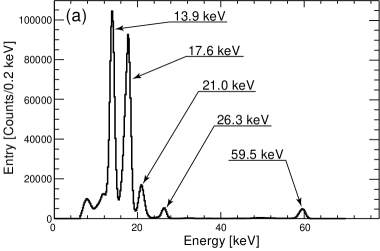
The energy resolution for -rays is investigated using the 59.54 keV -ray line from 241Am and the 122.06 keV -ray line from 57Co. The absolute gain is calibrated for each channel using the same -ray lines in such way that all channels give the nominal peak height. We also correct for the gain dependence on the “common mode shift” defined as the baseline shift common to all channels in one chip.¶¶¶The common mode shift is calculated and subtracted for each event taking the average of the pulse height for every channel, excluding the channels with signal. We attribute the origin of this dependence to the nonlinearity of the amplifier gain. A correction of approximately 0.2 keV is made for a 1 keV common mode shift. This correction is critical to operate the system at 20∘C, since the magnitude of the common mode shift is 6–10 keV at 20∘C and 1.6 keV at 0∘C. Larger common mode shift is observed for the longer peaking time at 20∘C, implying on a low frequency nature of the common mode shift. It should be noted that the peaking time of the fast shaper in the TA section is 0.3 s, which helps to suppress the contribution from common mode shift.
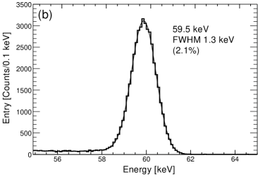
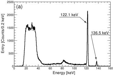
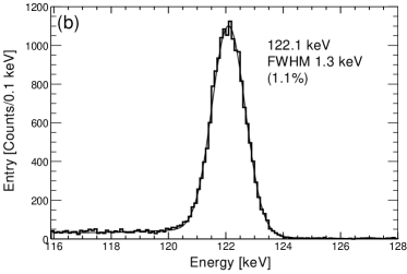
Figs. 5 (a) and 6 (a) show the sum of the energy spectra for all channels, except for the first and last strips where we observe larger noise. We observe a clear Compton edge just below 40 keV in the 57Co spectrum. In order to obtain the energy resolution, we fit the energy spectrum to a sum of two Gaussian functions to describe the peak and one threshold type function∥∥∥This function is expressed as . to describe the continuum spectrum. The second Gaussian is introduced to take into account the effect of the missing charge due to escaped electrons and charge sharing between strips. The mean value of the second Gaussian is shifted by 1–2 keV due to missing charge. The fraction of events in the second Gaussian is in general less than 15%. Figs. 5 (b) and 6 (b) show the magnified energy spectra around the peak and the fit results.
Table I summarizes the results of the energy resolution measurements. Energy resolution is worse than the intrinsic noise performance of the system. The fluctuation of the electron-hole pair generation degrades the energy resolution to 1.1 keV from 1.0 keV at 122 keV. The remaining contribution is predominantly due to the gain stability or uncertainty.
This result demonstrates that the energy resolution around 1 keV is an achievable goal, considering the planned improvements discussed below.
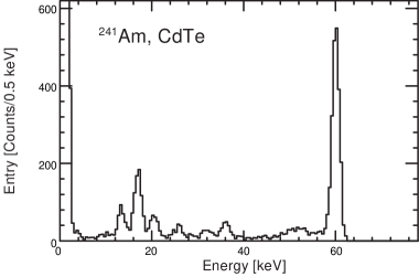
The VA32TA performance for a CdTe detector is also evaluated using an array of 2 mm 2 mm CdTe pixels. The thickness of the detector is 0.5 mm. Each pixel is connected to VA32TA via a fan-out board. Capacitance and leakage current of each pixel are 1 pF and a few pA at 0∘C. Low leakage current is realized by employing a guard ring to absorb leakage current from the detector edge [10]. Noise is measured to be 1.5 keV (FWHM). Fig. 7 shows the 241Am energy spectrum at a bias voltage of 600 V. We obtain an energy resolution of 1.7 keV (FWHM).
VI Conclusions and future prospect
We have developed a low noise front-end ASIC, VA32TA, for semiconductor Compton telescopes. Intrinsic noise performance with a silicon strip detector is measured to be 1.0 keV (FWHM) at 0∘C in the DC configuration, which is in good agreement with the analytically calculated noise value of 0.9 keV. The energy resolution is measured to be 1.3 keV (FWHM) for silicon strip detector and 1.7 keV for a CdTe pixel detector, demonstrating that the energy resolution around 1 keV is within our reach.
We plan to develop a full-size DSSD module based on the information obtained with the present prototype. The size of the DSSDs will be 5 cm 5 cm, which is the largest size possible with 4-inch wafers. This size translates into twice the capacitance load for amplifier in the DC configuration. Since the noise performance is dominated by the amplifier noise, improvements in the amplifier performance and reduction of the load capacitance is essential to achieve 1 keV energy-resolution. A low power version of the VA32TA, VA32TALP, is being developed by further optimizing the front-end MOSFET geometry in the 0.35 m process. The smaller feature size of the 0.35 m process enable us to reduce the FET channel length (), which in general improves the transconductance of the FET, i.e. noise performance [18]. Simulation studies indicate that ENC of (rms) can be achieved with m at a peaking time of 4 s despite the fact that the power consumption is reduced significantly to 0.2 mW/channel from 2 mW/channel. Approximately 10–20% improvement on the noise performance is expected by moving to m from m. We also plan to employ a thicker DSSD to reduce the capacitance to the backside.
In conclusion, we have demonstrated that energy resolution of silicon and CdTe detectors are as low as 1.3 keV and 1.7 keV, respectively, with the possibility of the future improvements. Such an ultra low noise ASIC presents great possibilities for future gamma-ray telescopes, such as the NeXT/SGD and SMCT.
References
- [1] V. Schöenfelder, H. Aarts, K. Bennett, H. de Boer, J. Clear, W. Collmar, et al., “Instrument description and performance of the imaging gamma-ray telescope COMPTEL abroad the Compton Gamma-Ray Observatory,” Astroph. J. Suppl. Series, vol. 86, pp. 657–692, 1993.
- [2] J. Knödlseder, P. von?allmoos, R. Diehl, U. Oberlack, V. Schöenfelder, H. Bloemen, W. Hermsen, J. M. Ryan, and K. Bennett, “COMPTEL gamma-ray line analysis techniques,” in Gamma-Ray and Cosmic-Ray Detectors, Techniques, and Missions, SPIE, B. D. Ramsey and T. A. Parnell, Eds., vol. 2806, 1996, pp. 386–397.
- [3] T. Kamae, R. Enomoto, and N. Hanada, “A new method to measure energy, direction, and polarization of gamma rays,” Nucl. Instrum. Methods A, vol. 260, pp. 254–257, 1987.
- [4] T. Kamae, N. Hanada, and R. Enomoto, “Prototype design of multiple Compton gamm-ray camera,” IEEE Trans. Nucl. Sci., vol. 35, pp. 352–355, 1988.
- [5] T. Takahashi, T. Kamae, and K. Makishima, “Future hard X-ray and gamma-ray observations,” in New Century X-ray Astronomy, ASP (Astronomical Society of the Pacific Conference Series), vol. 251, 2002, pp. 210–213.
- [6] T. Takahashi, K. Makishima, F. Fukazawa, M. Kokubun, K. Nakazawa, M. Nomachi, H. Tajima, M. Tashiro, and Y. Terada, “Hard X-ray and Gamma-ray detectors for the next mission,” New Astro. Rev., vol. 48, pp. 309–313, 2004.
- [7] P. F. Bloser, R. Andritschke, G. Kanbach, V. Schöenfelder, F. Schopper, and A. Zoglauer, “The MEGA advanced Compton telescope project,” in New Astronomy Reviews (Proceedings of the Ringberg Workshop “Astronomy with Radioactivities III”), astro-ph/0110129, 2001.
- [8] P. A. Milne, R. A. Kroeger, J. D. Kurfess, and L.-S. The, “Advanced Compton telescope designs and SN science,” in New Astronomy Reviews (Proceedings of the Ringberg Workshop “Astronomy with Radioactivities III”), astro-ph/0110346, 2001.
- [9] T. Takahashi, S. Watanabe, M. Kouda, G. Sato, Y. Okada, S. Kubo, Y. Kuroda, M. Onishi, and R. Ohno, “High-resolution CdTe detector and applications to imaging devices,” IEEE Trans. Nucl. Sci., vol. 48, pp. 287–291, 2001.
- [10] K. Nakazawa, T. Takahashi, Y. Kobayashi, T. Mitani, T. Tanaka, K. Oonuki, G. Sato, S. Watanabe, R. Ohno, A. Kitajima, Y. Kuroda, and M. Ohnishi, “Improvement of the CdTe diode using a guard-ring electrode.” IEEE Trans. Nucl. Sci., 2004 (to be published).
- [11] H. Tajima, “Gamma-ray polarimetry,” Nucl. Instrum. Methods A, vol. 511, pp. 287–290, 2003.
- [12] T. Mitani, T. Tanaka, K. Nakazawa, T. Takahashi, T. Takashima, H. Tajima, h. Nakamura, M. Nomachi, T. Nakamoto, and Y. Fukazawa, “Prototype of Compton camera using high resolution Si/CdTe detectors,” in Proceedings for IEEE Nuclear Science Symposium, 2003.
- [13] E. Nygård, P. Aspell, P. Jarron, P. Weilhammer, and K. Yoshioka, “CMOS low noise amplifier for microstrip readout design and results,” Nucl. Instrum. Methods A, vol. 301, pp. 506–516, 1991.
- [14] O. Toker, S. Masciocchi, E. Nygård, A. Rudge, and P. Weilhammer, “VIKING, a CMOS low noise monolithic 128 channel frontend for Si-strip detector readout,” Nucl. Instrum. Methods A, vol. 340, pp. 572–579, 1994.
- [15] M. Yokoyama, H. Aihara, M. Hazumi, H. Ishino, J. Kaneko, Y. Li, D. Marlow, S. Mikkelsen, E. Nygård, H. Tajima, J. Talebi, G. Verner, and H. Yamamoto, “Radiation hardness of VA1 with sub-micron process technology,” IEEE Trans. Nucl. Sci., vol. 48, pp. 440–443, 2001.
- [16] S. Korpar, P. Križan, and S. Frantina, “SEU studies of the upgraded Belle vertex detector front end electronics,” Nucl. Instrum. Methods A, vol. 511, pp. 195–199, 2003.
- [17] H. Tajima, T. Kamae, S. Uno, T. Nakamoto, Y. Fukazawa, T. Mitani, T. Takahashi, K. Nakazawa, Y. Okada, and M. Nomachi, “Low noise double-sided silicon strip detector for multiple-Compton gamma-ray telescope,” in X-ray and Gamma-ray Telescopes and Instruments for Astronomy, SPIE, J. E. Truemper and H. D. Tananbaum, Eds., vol. 4851, 2002, pp. 875–884 (SLAC–PUB–9493, ISAS–RN–754, astro–ph/0 212 053).
- [18] P. O’Connor and G. D. Geronimo, “Prospect for charge sensitive amplifiers in scaled CMOS,” Nucl. Instrum. Methods A, vol. 480, pp. 713–725, 2002.