Role of on-site Coulomb energy and negative-charge transfer in a Dirac semi-metal
Abstract
Angle-resolved photoemission spectroscopy in combination with band structure calculations have shown that the layered transition metal dichalcogenide NiTe2 is a type-II Dirac semimetal. However, there are conflicting conclusions in the literature regarding the role of electron correlations in NiTe2. We study the core-level and valence band electronic structure of single crystal NiTe2 using soft and hard X-ray photoemission spectroscopy (SXPES, HAXPES), X-ray absorption spectroscopy (XAS) and Ni resonant photoemission spectroscopy(resonant-PES) to quantify electronic parameters in NiTe2. The on-site Coulomb energy () in the Ni states is quantified from measurements of the Ni single particle density of states and the two-hole correlation satellite. The Ni core level and -edge XAS spectra are analyzed by charge transfer cluster model calculations using the experimentally estimated (= 3.7 eV), and the results show that NiTe2 exhibits a negative charge-transfer energy ( = -2.8 eV). The same type of cluster model analysis of NiO -edge XAS confirms its well-known strongly correlated charge-transfer insulator character, with = 7.0 eV and = 6.0 eV. The - hybridization strength for NiTe2NiO, and indicates that the reduced in NiTe2 compared to NiO is not due to an increase in . The increase in count on the Ni site in NiTe2 by nearly one electron is attributed to negative- and a reduced . However, since , the results indicate the important role of a finite repulsive in making NiTe2 a moderately correlated -type Dirac semi-metal.
I Introduction
The experimental discovery of topological insulators (TIs) can be considered a major turning point in condensed matter studies and was achieved by: (i) observing a transition from a conventional insulator to a Quantum Spin Hall insulator with a pair of gapless helical edge-states in HgTe/(Hg,Cd)Te quantum wells using transport measurementsMolenkamp , and (ii) from observation of metallic surface states exhibiting spin-textured linear Dirac-type band dispersions in the surface electronic structure of a 3-dimenional (3D) bulk insulating material Bi1-xSbx using angle-resolved photoemission spectroscopy(ARPES)Hsieh2008 .
The experimental discoveries confirmed theoretical predictions of these fascinating transport properties and the electronic structure of the TIs, including the Quantum Spin Hall effect, time-reversal invariance and Dirac-type metallic surface state band dispersions inside a bulk charge gap induced by spin-orbit coupling (SOC) with band inversionMurakami ; Kane ; Bernevig ; Fu2007 ; Moore ; Roy ; Zhang . The relevance of inverted band gaps in substituted semiconductors like Pb1-xSnxTe and Hg1-xCdxTe leading to Dirac/Weyl type bands in the gap was recognized earlierVolkov ; Pankratov and the importance of inverted band-gaps for the spin Hall effect in semiconductors such as HgTe, HgSe and -HgS as well as for PbTe, PbSe and PbS was pointed out in ref.Murakami .
Several materials were soon reported to show a single Dirac cone in materials like Bi2Se3, Bi2Te3, Sb2Te3, etc. using ARPES experimentsXia2009 ; Chen2009 ; Hsieh2009 . Similarly, the three-dimensional (3D) Weyl semimetal (WSM) phase was predicted based on theoretical calculations of a multilayer consisting of magnetically doped 3D TI films alternating with ordinary-insulator layers, leading to a topological phase with a band structure possessing a pair of Dirac/Weyl nodes of opposite chirality, separated in momentum()-spaceBB . The WSM was also predicted to show topologically protected edge states, a finite dc conductivity at zero temperature and a Drude weight vanishing as T2, and experiments on the pyrochlore Eu2Ir2O7 confirmed qualitative agreementSushkov . On the other hand, ARPES studies confirmed the characteristic Fermi arcs connecting the Dirac/Weyl nodes, as shown in TaAsLv ; Huang and NbPSouma . The WSMs require broken time-reversal symmetry and/or can have broken inversion symmetryZyuzin . In contrast, the Dirac semimetals(DSMs) form when both, time reversal and inversion symmetries are presentBurkov ; Bahramy . They can be of two types: Type I DSMs, which obey Lorentz symmetry and show regular Dirac-type linear dispersions along all three directions in -space as was seen in Na3BiLiu ; Xu and Cd3As2Neupane ; Borisenko , and Type II DSMs, which violate Lorentz symmetry and show tilted Dirac cones and form a Dirac point in -space at which an electron and a hole pocket touch each otherBurkov ; Bahramy . While these materials are called semimetals in relation to their -resolved relatively small electron- and hole-pockets, due to their high mobilities, the actual conductivity of these materials are quite high.
For NiTe2, a very high conductivity of (T = 2 K)1.0106S/m has been reportedShi . Regarding magnetic behavior, magnetic susceptibility measurements do not show evidence for magnetic ordering down to T = 2 K but instead show a Pauli paramagnetic behavior.Mao . It is known that the NiTe2-x series exhibits pressure-induced superconductivity8 . NiTe2-x nanomaterials have also been reported to work as electrocatalysts for hydrogen evolution reactionShi ; 10 . In a very recent study, it was shown that NiTe2 is a topological superconductor with a very low = 261 mKCHe .
Several layered transition metal dichalcogenides, such as PtSe2, PdTe2, PtTe2, CoTe2 and NiTe2 to name a few, have shown Type II DSM behaviorBahramy ; Zhang2017 ; Noh ; Yan ; Clark ; Chakraborty2023 ; Xu2018 ; Ghosh2019 ; Mukherjee ; hlevyack2021 ; Nurmamat ; Fischer ; Bhatt_2025 . In particular, it has been shown that a bulk Type-II Dirac point lies at an energy of 0.5 eV, 0.9 eV and 1.5 eV below the Fermi level() in PdTe2, PtTe2 and PtSe2, respectivelyBahramy ; Zhang2017 ; Noh ; Yan ; Clark . For CoTe2, the bulk Type-II Dirac point lies 0.9 eV above while a Dirac point in surface states lies 0.5 eV below Chakraborty2023 . In contrast, the bulk Type-II Dirac point in NiTe2 was reported to lie 20-68 meV above by three groupsGhosh2019 ; Mukherjee ; hlevyack2021 , while one group reported it to lie 150 meV below Nurmamat . NiTe2 also shows surface states just at , and another Dirac-like crossing lies far (1.5 eV) below Ghosh2019 ; Mukherjee ; hlevyack2021 ; Nurmamat ; Bhatt_2025 .
However, while three different studies on NiTe2 using ARPES and band structure calculations had ruled out the relevance of correlation effects in NiTe2Ghosh2019 ; Mukherjee ; hlevyack2021 , two very recent studies have concluded the importance of correlations for the Te - derived bands in NiTe2Fischer ; Bhatt_2025 . In one case, Fischer et al.Fischer carried out DFT calculations to obtain the band structure and then applied many-body effects within the GW approximation. They found anisotropic improvement in the Te bands with an increase in Dirac carrier velocity exceeding 100% and emphasized the subtle influence of electronic interactions on the band structure. In contrast, Bhatt et al.Bhatt_2025 used LDA+U (with U = 5 eV) and concluded that the topological Te surface states lying 1.5 eV below can be described only by including U. Surprisingly, there is no discussion of how the Ni states are modified due to correlation effects in NiTe2 to date. Since Ni is divalent in NiTe2 as the Te atoms are dimerized (Te)Jobic ; bensch1996 , if we consider the example of divalent NiO which is known to be a strongly correlated charge-transfer insulator, one can expect that Ni2+ states in NiTe2 may also be correlated. However, it may be expected to be less correlated than NiO since it was shown that NiTe2 is a Pauli paramagnetic metalZheng . The same study carried out bulk sensitive dHvA experiments and showed that individual bands had to be shifted in a somewhat ad-hoc manner (one with an energy shift of -60 meV, and another with a shift of +100 meV) to match with measured dispersions, and discrepancies were also found in calculated and measured values of light and nearly isotropic effective masses. The authors concluded that their results indicated DFT calculations failed to capture the finer details of the electronic band structure of NiTe2Zheng .
In this work, we carry out photoemission spectroscopy, XAS and Ni resonant PES to quantify electronic parameters in NiTe2. We quantify the on-site Coulomb energy () in the Ni states using experimentally obtained Ni single particle density of states and the two-hole correlation satellite. From an analysis of the Ni core level and -edge XAS spectra using charge transfer cluster model calculations using the experimentally estimated , we find that NiTe2 is a negative charge-transfer energy material with = -2.8 eV). We carry out a similar cluster model analysis of NiO -edge XAS to compare electronic parameter values. The results show = 3.7 eV and the charge transfer energy = -2.8 eV for NiTe2, while the corresponding values are = 7.0 eV and = 6.0 eV for NiO. The obtained values of - hybridization strength indicate it is smaller for NiTe2 compared to NiO. Since , it indicates the important role of a moderate repulsive in making NiTe2 a topological metal with pp type lowest energy excitations in the Zaanen-Sawatzky-Allen (ZSA) scheme zaanen1985 .
II Methods
II.1 Synthesis and structure characterization
The single crystals of NiTe2 were prepared by the chemical vapor transport method, using iodine as the transport agentProdan . High-purity Ni (99.95%) and Te (99.999%) powders were mixed with a small amount of iodine (40 mg), sealed in an evacuated quartz tube, and then heated for 10 days in a two-zone furnace. Finally, the quartz tube was quenched into an ice-water bath from the growth temperature of 800∘C. The obtained single crystals are hexagonal in shape with typical dimensions of 4 mm4 mm0.5 mm. The crystal structure was characterized using powder X-ray diffraction (XRD) (Bruker D2 phaser diffractometer) with Cu-K radiation. The single crystal quality was confirmed and crystallization directions were identified by the Laue diffraction method (Photonic Science). The XRD results confirmed the 1T-CdI2-type trigonal structure (space group of Pm1 (No. 164)) with the flat-surfaces corresponding to the (001) plane. The obtained lattice parameters of NiTe2 are = 3.853 and = 5.260. These values are very close to reported values of = 3.843 and = 5.266TMdatabase .
II.2 Electron spectroscopy
Hard X-ray photoemission spectroscopy (HAXPES) core levels and valence band measurements were carried out at BL-12XU (Taiwan Beamline), SPring8, Japan using linearly polarized X-ray beam with incident photon energy = 6.5 keV. Liquid He closed cycle cryostat was used to cool down the sample to T = 25 K. The of Au thin film was measured at 25 K to calibrate the binding energy (BE) scale and determine the total energy resolution ( E = 270 meV) from a fit to the Au film Fermi edge. NiTe2 single crystal was cleaved using a top-post in ultra-high vacuum (UHV) at 5.5 10-9 mbar in the preparation chamber and then quickly transferred to the main chamber at 7.0 10-10 mbar for the measurements. Soft X-ray PES (SXPES) core level and valence band, XAS and 2 resonance PES measurements were carried out at BL-17SU, RIKEN beamline in SPring8, Japan using a circularly polarized X-ray beam. The Ni -edge and Te -edge XAS measurements were carried out in total electron yield mode. SXPES core levels and valence band measurements were carried out with incident photon energy = 1.5 keV. A Liquid N2 flow-type cryostat was used to cool the sample down to 80 K. The total energy resolution for SXPES was E = 400 meV, as obtained from a fit to the Au Fermi edge measured with = 1.5 keV at T = 80 K. Sample was cleaved in the main chamber at a UHV better than 1.0 10-10 mbar. The resonant PES spectra were normalized at the Te 4 core level peaks.
II.3 Cluster-model calculations
The Ni 3,2-edge XAS and Ni 2 PES core level spectra were calculated using a charge transfer multiplet cluster model with the QUANTY codehaverkort2012 ; lu2014 ; haverkort2014 . A Ni cluster with divalent Ni2+ ion (3) and 6 ligand() atoms of Te in octahedral symmetry () was used to calculate the spectra. The initial state consists of a linear combination of , and states, where L corresponds to hole in ligand states. The value of was fixed to 3.7 eV as obtained from the Cini-Sawatzky analysis, while , the hybridization strength ( and = /2) and the crystal field splitting 10 were varied to obtain calculated spectra close to experimental spectra. The calculated spectra were obtained by convoluting the discrete final states by broadening it with a Lorentzian function for lifetimes and a Gaussian function for the experimental spectral width.
III results and discussion
| Fit component | Binding Energy | FWHM |
|---|---|---|
| SXPES | (eV) | (eV) |
| Ni 2 | 853.62 | 1.12 |
| Ni 2 | 870.87 | 1.12 |
| Te 3 | 819.44 | 3.5 |
| Te 3 | 870.44 | 3.5 |
| Ni 2 Satellite | 860.30 | 5.5 |
| Ni 2 Satellite | 877.51 | 5.0 |
| Ni 2 Plasmon | 872.80 | 7.5 |
| Te 3 Plasmon | 838.66 | 11.40 |
| Te 3+Ni 2Plasmon | 889.78 | 13.96 |
| HAXPES | ||
| Ni 2 | 853.42 | 1.01 |
| Ni 2 | 870.67 | 1.01 |
| Te 3 | 819.40 | 3.94 |
| Te 3 | 870.40 | 3.94 |
| Ni 2 Satellite | 860.10 | 5.3 |
| Ni 2 Satellite | 877.32 | 4.5 |
| Ni 2 Plasmon | 872.78 | 6.0 |
| Te 3 Plasmon | 838.66 | 11.19 |
| Te 3+Ni 2 Plasmon | 889.72 | 9.76 |
Figure 1 shows the Ni 2 and Te 3 core level range from 812 - 900 eV BE measured with HAXPES ( = 6.5 keV) and SXPES ( = 1.5 keV). The spectra show three high intensity peaks instead of the expected four peaks: Ni 2, Ni 2, Te 3 and Te 3, together with weak features. However, we can accurately identify the BE positions and spin-orbit (SO) splitting of the high intensity main peaks of Te 3 (819.4 eV) - Te 3 (869.9 eV) doublet from known reference dataXPShandbook as well as our CoTe2 measurementsShelkeCoTe2 . Similarly, we also know the SO splitting of the Ni 2-Ni 2 doublet and can also identify the Ni 2 main peak at 853.6 (eV) (consistent with a recent measurementnappini2020 ), and then it is understood that the broader Te 3 main peak is overlapping and masks the Ni 2 main peak, expected at 872.9 eV XPShandbook . Further, as the HAXPES and SX-PES spectra have been normalized at the Te 3, it can be seen that the Ni 2 shows significantly higher intensity compared to Te 3p states in SX-PES data due to its higher photo-ionization cross-section compared to HAXPES datatrzhaskovskaya2018 .
In order to characterize the details of the independent contributions of Ni 2 and Te 3 main peaks, as well as that of the weaker features, we carried out a least-squares fitting by considering the SO splitting energies of 19.3 eV and 50.5 eV for Ni 2 and Te 3, respectivelyXPShandbook . Since the Te 3 and Te 3 shows broad satellites at 19.7 0.1 eV, and similar features at 19.7 higher BEs are also seen in Te spectra (Fig. 3), we assign them to plasmon excitations. For the fitting, we constrained the intensity ratios of Ni 2 : Ni 2 and Te 3 : Te 3 to the expected value of 2 : 1 and used asymmetric Doniach-Sunjic Voigt lineshapes for the main peaks and charge-transfer satellites, and symmetric Gaussians for the plasmon features. However, since the Ni 2 main peak shows a satellite about 8 eV higher BE, it indicates the Ni 2p peaks also show a charge transfer(CT) satellite similar to other known Nickel compounds. Accordingly, just above the Ni 2, we used an asymmetric Voigt function for the CT satellite while just above the Ni 2 main peak, we included one Gaussian for the Ni 2 main peak plasmon and another asymmetric Voigt function for the weaker CT satellite. The fits to the Ni 2 and Te 3 for both SXPES and HAXPES are shown in Fig. 2(a) and (b), respectively, and the obtained BEs and their full-width and half-maximum (FWHM) are listed in Table I. The main peak BEs are very similar for Ni 2 and Te 3 core levels in both, SXPES and HAXPES data.
| Fit component | Binding Energy | FWHM |
|---|---|---|
| SXPES | (eV) | (eV) |
| Te 3 | 572.72 | 0.82 |
| Te 3 | 583.13 | 0.88 |
| Te 3 Plasmon | 591.90 | 7.5 |
| Te 3 Plasmon | 602.32 | 4.5 |
| HAXPES | ||
| Te 3 | 572.62 | 0.72 |
| Te 3 | 583.01 | 0.74 |
| Te 3 Plasmon | 591.82 | 7.0 |
| Te 3 Plasmon | 602.21 | 4.5 |
In Fig. 3(a) and (b), we show the Te 3 core levels measured using HAXPES and SXPES, respectively. The spectra show two sharp single peaks for Te 3 and Te 3 main peaks and plasmon features at higher BEs. A least-squares fitting to the Te 3 and Te 3 main peaks and plasmon features is superimposed as full lines on the experimental spectra (empty circles). The main peaks were fitted with single asymmetric Voigt functions, and the plasmon features with symmetric Gaussian functions. The peak BEs and FWHMs are listed in Table II. The Te 3 and Te 3 main peaks are at 572.72 eV 0.1 eV and at 583.13 eV 0.1 eV in SXPES and HAXPES spectra. The observed BE values are very consistent with reported values of Te 3 core levels of NiTe2 bensch1996 ; nappini2020 . The sharp single main peaks of Te 3 and Te 3 and absence of any feature 3.0 eV above the main peaks indicates absence of oxidation in SXPES and HAXPES spectranappini2020 . Further, the broad low intensity features are positioned at 19.7 eV 0.1 eV higher BEs and confirm their plasmon origin, consistent with Te 3 SXPES and HAXPES core levels.
We then carried out Ni 2 - 3 resonant-PES of NiTe2 to quantify the experimental value of from measurements of the single particle 3 partial density of states (PDOS) and the two hole correlation satellite using the Cini-Sawatzky method cini1976 ; cini1977 ; sawatzky1977 . Fig. 4(a) shows the Ni resonant PES valence band intensity map as a function of photon energies ( = 849-879 eV) versus BE ( = -1.2 to 45.8 eV). The resonant PES map is obtained by first measuring the Ni -edge XAS Fig. 4(b) as a function of (top X-axis). Then, at different incident photon energies marked by arrows in the XAS spectrum(Fig. 4(b)), we measure the valence band spectra and plot the spectral intensity as the map shown in Fig. 4(a). Fig. 4(c) shows valence band spectra (BE = -1.2 eV to 35.0 eV) measured at select values (labelled ) across the and edge of Fig. 4(b). The BEs are calibrated with respect to of metallic NiTe2 and the spectra are normalized to the shallow Te 4 core level peaks (bright blue vertical lines at 41 and 42 eVBEs) in the map. Several well-resolved spectral features derived from Ni bands and Te 5 bands are observed in the valence band spectra. The weak spectral feature at 1.90 eV BE shows a small increase in intensity when incident values just cross the and edges and indicate a weak Ni 2 resonance of the Ni 3 derived partial density of states (PDOS) orders1982 (yellow vertical line observed in map and also marked in Fig. 4(c)). The central feature in the Fig. 4(a) map is the diagonal from right bottom to left top. It originates in a feature at 7.90 eV BE in the map and Fig. 4(c), and shows a significantly large increase in intensity on increasing from , i.e., upto the Ni -edge maxima (blue vertical dotted line in the map and Fig. 4(c). On increasing further from , this feature systematically moves to higher BEs with a shift equal to the increase in . This behavior of shift in BE equal to increase in indicates its Ni Auger feature (marked by the blue diagonal line in the map and in Fig. 4(c)). Fig. 4(d) shows a plot of the kinetic energy of this peak as a function of relative to the XAS peak energy (bottom X-axis). The corresponding incident values are the same as top X-axis of Fig. 4(b). This indicates that the 7.90 eV constant BE feature for = represents a resonant Raman feature and it becomes a correlation satellite with two holes in the final stateguillot1977 ; weinelt1997 ; hufner2000 . The map and Fig. 4(c) also shows a weak broad feature at 19.3 eV BE for across the Ni edge, which is attributed to a plasmon feature as seen in core level spectra. For higher from , the map and Fig. 4(c) again show a weak resonant Raman behavior(blue vertical dotted line), followed by the two-hole correlation satellite Auger peak (blue full line) of the 7.90 eV BE feature. The corresponding kinetic energy of this peak as a function of is also plotted in Fig. 4(d) and confirms its Auger character.
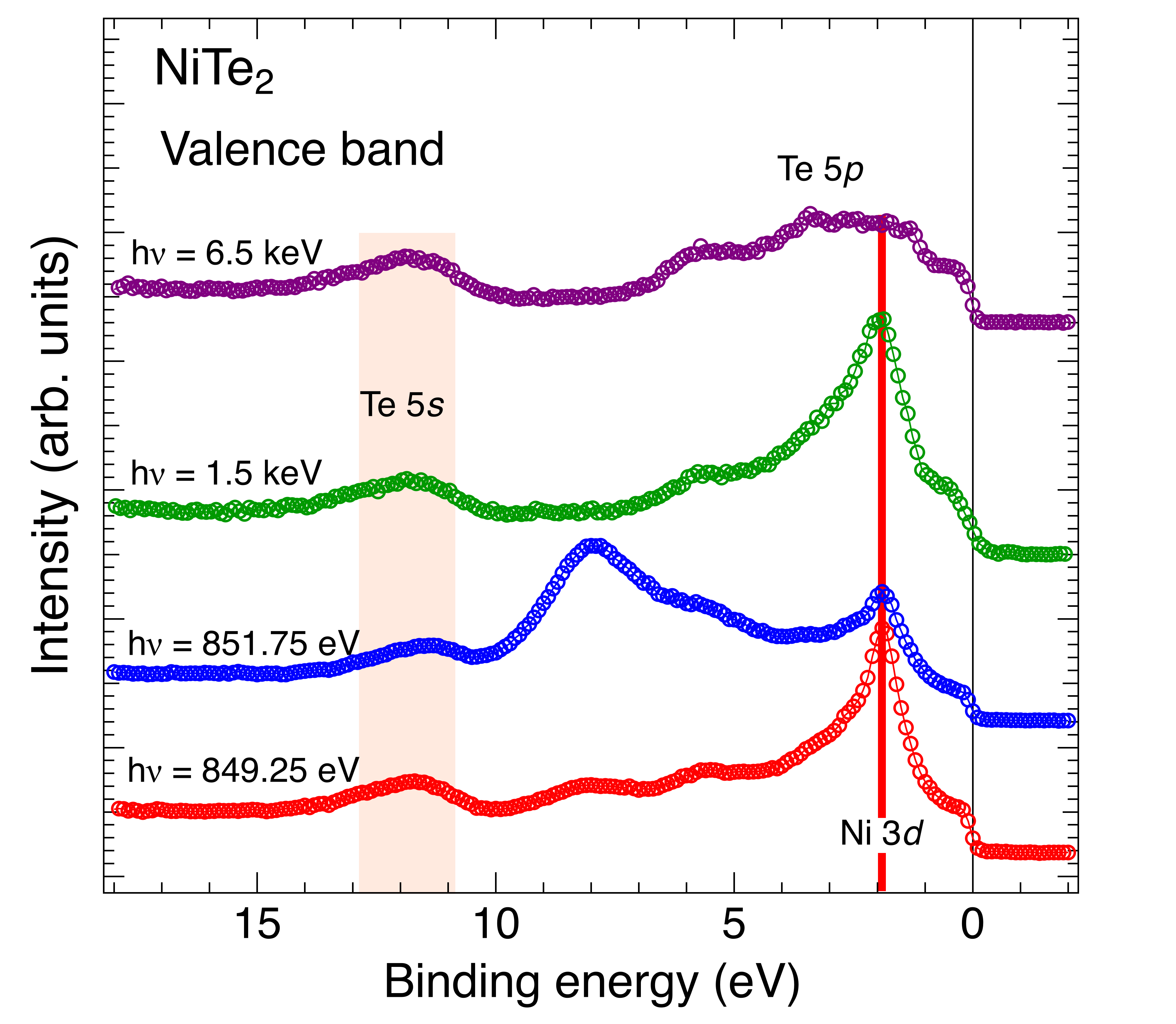
Figure 5 shows the valence band spectra measured at three different off-resonant photon energies of values = 849.25 eV,1.5 keV, 6.5 keV, and one in the Resonant Raman region with = 851.75 eV. All these spectra are normalized at the broad spectral feature at 11.5 eV BE, which corresponds to the Te 5 shallow core level, with the purpose of emphasizing the relative spectral weights of Te 5 states and Ni 3 states. Comparison of the spectra obtained with the two lowest values, indicates that the Ni 3d PDOS peak at 1.90 eV BE in Fig. 5 shows a weak suppression in the Resonant Raman region ( = 851.75 eV) but the two-hole satellite at 7.9 eV BE gets enhanced, when compared to the off-resonant ( = 849.25 eV) spectrum. However, the spectral shape recovers at the higher off-resonant =1.5 keV and becomes fairly similar to = 849.25 eV. On the other hand, at = 6.5 keV, the 1.90 eV BE and 7.9 eV BE features get strongly suppressed at = 6.5 keV due to the strongly reduced PICS of Ni 3 states compared to the Te 5 states at = 6.5 keVtrzhaskovskaya2018 . At = 6.5 keV, the Te 5 states dominate the spectrum as the PICS ratio of Te 5 : Ni 3 is 6.41 trzhaskovskaya2018 . This indicates that the feature at EF corresponds to dominantly Te PDOS. This is consistent with reported DFT electronic structure calculations and ARPES measurements which concluded that Te states lie at and within 0.5 eV BE Ghosh2019 ; Mukherjee ; hlevyack2021 ; Nurmamat ; settembri2024 ; Bhatt_2025 . As we will show in Fig. 7 below, this observation is also consistent with a negative in NiTe2. Before that, we quantify using the Cini-Sawatzky methodcini1976 ; cini1977 ; sawatzky1977 applied to the experimental Ni 3 PDOS and two-hole correlation satellite data.
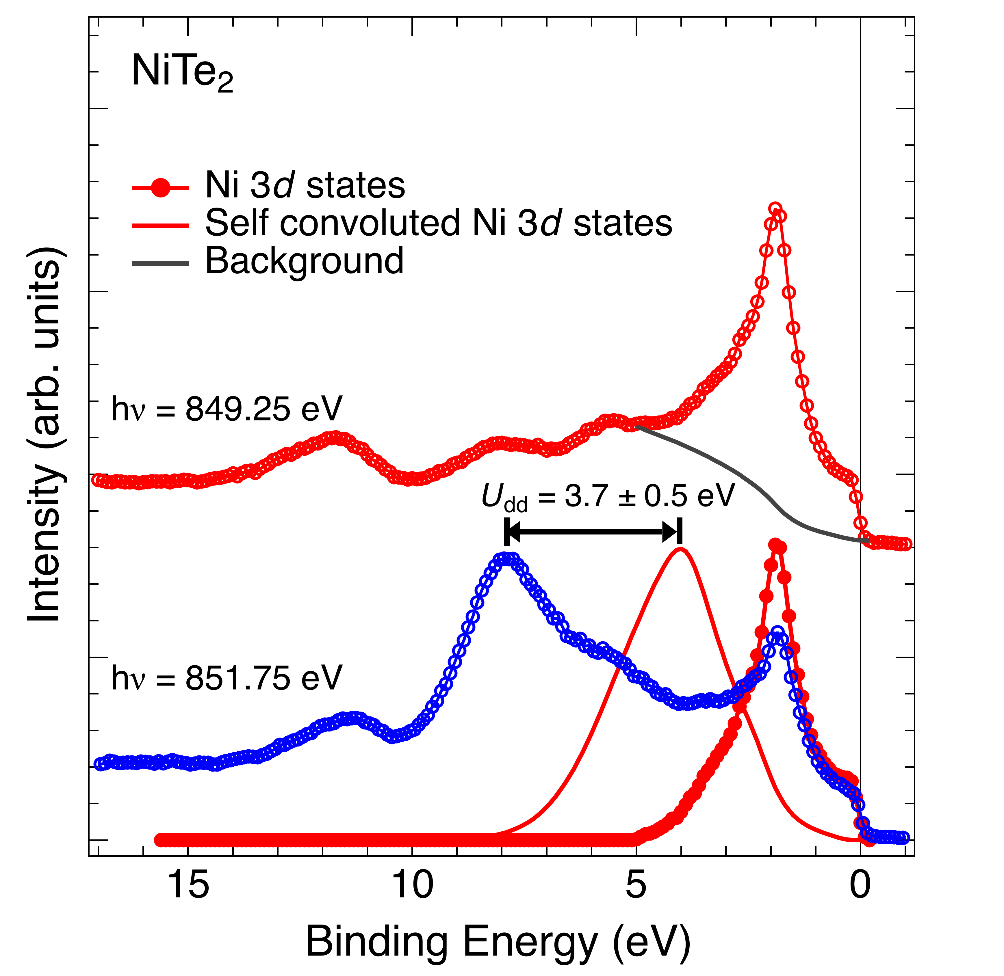
Figure 6 shows the off resonance spectrum obtained with = 849.25 eV before/after (red /) subtracting an integral background in order to separate out the single-particle Ni 3 PDOS from the Te 5 states at higher BEs. The single-particle PDOS was then numerically self-convoluted to obtain the two-hole spectrum (red line), and its peak energy represents the average two-hole energy without correlations. This two hole spectrum was then compared with the spectrum exhibiting the experimental two-hole correlation satellite spectrum in the resonant Raman region ( = 851.75 eV; blue color ). In the Cini-Sawatzky method, the energy difference between the peak in the two-hole spectrum without correlations and the peak of the experimental two-hole correlation satellite gives an estimate of the on-site Coulomb energy . We obtain the value of = 3.7 eV for Ni 3 states, indicating that the NiTe2 is a moderately correlated metal. In the following, we use the obtained value in charge-transfer cluster model calculations to simulate the Ni 2 core-level PES and -edge XAS spectra of NiTe2 to independently check its validity.
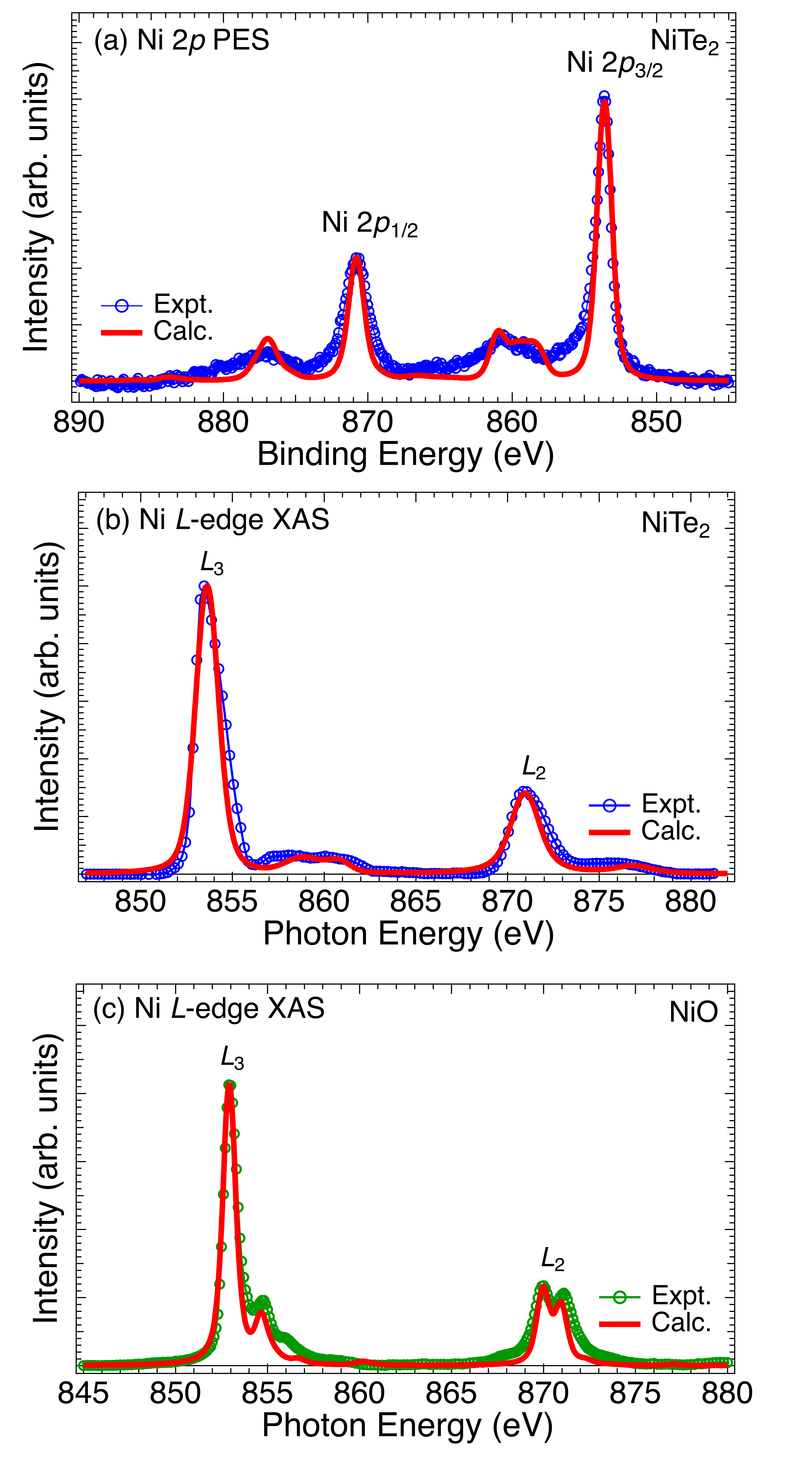
Figures 7(a) and (b) show the experimental Ni 2 PES core level and Ni -edge XAS spectra of NiTe2 compared with charge transfer cluster model simulations obtained using = 3.7 eV and optimizing other electronic parameters, as described in Methods section. Due to the overlapping Ni 2 and Te 3 peaks, the experimental Ni 2 PES core level spectrum shown in FIg. 7(a) was obtained by subtracting out the fits to the Te 3 main peak and its plasmon, as well as the Ni 2 plasmon fit. For the Ni -edge XAS shown in Fig. 7(b), since the Te M5-edge region did not show significant intensity in the XAS spectrum due to very low cross-section, we did not need to subtract a corresponding feature for the Te M4-edge region. We confirmed that the spectral lineshape of Ni -edge XAS shown in Fig. 7(b) is very similar to the reported Ni -edge XAS of NiTe2 single-crystal cleaved surface, including the satellite structures for the Ni -edge nappini2020 . We then carried out an extensive set of calculations by varying , , (=/2) and 10 to optimize the parameters(see appendix). Using the experimental = 3.7 eV, and the same set of optimized parameters as listed in Table III, we could obtain calculated spectra close to the experiment for both Ni 2 PES and Ni -edge XAS spectra. Similarly, using = 7.0 eV (from earlier XAS calculations for NiO; ref.Veenendaal ; alders1998 ), we optimized the other parameters for Ni -edge XAS spectrum of NiO (listed in Table III) to obtain a calculated spectrum close to experiment.
The comparison of electronic parameters for NiTe2 and NiO, spin magnetic moments, counts and individual weights in Table III indicates that NiTe2 is a moderately correlated negative charge-transfer metal in the Zaanen-Sawatzky-Allen (ZSA) scheme zaanen1985 , while NiO is a positive charge-transfer insulator as is well-knownFujimoriNiO ; VeenendaalPRL ; Veenendaal ; alders1998 ; Ghiasi . It is noted that while the NiO Ni -edge XAS can be reproduced fairly with a single metal site cluster model calculationVeenendaal ; alders1998 , the Ni 2p core level PES was shown to require a multiple Ni-site calculationVeenendaalPRL , or a single metal-site CT multiplet calculation combined with DMFT calculationsGhiasi , to reproduce the additional well-screened peak observed in 2p PES arising from non-local screening. Further, we confirmed that the ground state of NiO consists of a mixture of 85.0% , 14.6% and a very small contribution of 0.4% weights, consistent with the early study of Fujimori and Minami which showed NiO has a ground state consisting of a mixture of 83.0% and 17.0% weightsFujimoriNiO .
In contrast, the ground state of NiTe2 consists of a mixture of 19.5% , 57.4% and a 23.1% weights. The negative- for NiTe2 also implies that the lowest energy excitations are pp type excitations, consistent with ARPES resultsGhosh2019 ; Mukherjee ; hlevyack2021 ; Nurmamat ; settembri2024 ; Bhatt_2025 . The obtained values of - hybridization strength indicate that is smaller for NiTe2 compared to NiO, consistent with Ni-Te distance (= 2.620) being larger than Ni-O distance (= 2.09). This indicates that the reduced in NiTe2 compared to NiO is not due to an increase in . The large increase in count on the Ni site ( = 9.1) by more than one electron compared to a formal = 8 for divalent NiTe2 is attributed to negative- and a reduced . A detailed analysis of the relation of with and using CT cluster model calculations is presented in ref.ShelkeCoTe2 . While the value of in NiTe2 gets reduced by 50% compared to NiO, the moderately repulsive value of = 3.7 eV is crucial to achieve topological properties in NiTe2 as follows: if was , NiTe2 would exhibit a Mott-Hubbard character with dd type lowest energy excitations in the ZSA phase diagramzaanen1985 , and would not be a topological Dirac semi-metal. Thus, only because , NiTe2 becomes a topological Dirac semi-metal with pp type excitations between strongly spin-orbit coupled Te derived states.
| Parameter | NiTe2 | NiO |
|---|---|---|
| (eV) | 3.7 | 7.0 |
| (eV) | -2.8 | 6.0 |
| (eV) | 1.8 | 2.4 |
| (eV) | 0.9 | 1.2 |
| (eV) | 0.5 | 1.65 |
| , | 1.0 | 0.8 |
| () | 0.96 | 1.82 |
| count | 9.1 | 8.14 |
IV Conclusions
In conclusion, the core-level and valence band electronic structure of single crystal NiTe2 was investigated for quantifying electronic parameters in NiTe2. Using the Cini-Sawatzky method, we obtain a value of = 3.7 eV. The Ni core level and -edge XAS spectra were analyzed by charge transfer cluster model calculations using the obtained (= 3.7 eV), and the results indicate NiTe2 is a negative charge-transfer material with = -2.8 eV. The same type of cluster model analysis for NiO -edge XAS confirms its well-known strongly correlated charge-transfer insulator character, with = 7.0 eV and = 6.0 eV. The hybridization strength between Ni and ligand states for NiTe2NiO, and indicates that the reduced in NiTe2 compared to NiO is not due to an increase in . The count on the Ni site increases by nearly one electron in NiTe2 due to negative- and a reduced . Since , the results indicate the important requirement of a finite repulsive in making NiTe2 a moderately correlated -type Dirac semi-metal.
Acknowledgements.
This work was supported by the National Science and Technology Council(NSTC) of Taiwan under Grant Nos. NSTC 113-2112-M-006-009-MY2 (CNK), 110-2124-M-006-006-MY3 (CSL), 112-2124-M-006-009 (CSL), 113-2112-M-007-033 (AF), 112-2112-M-213-029(AC) and 114-2112-M-213-021(AC). AF acknowledges support from the Yushan Fellow Program under the Ministry of Education of Taiwan and Grant No. JP22K03535 from Japan Society for the Promotion of Science(JSPS). ARS thanks the National Science and Technology Council(NSTC) of Taiwan for a post-doctoral fellowship under Grant No. NSTC 114-2811-M-213-006.Appendix A Optimization of electronic parameters in cluster model calculations of NiTe2 and NiO
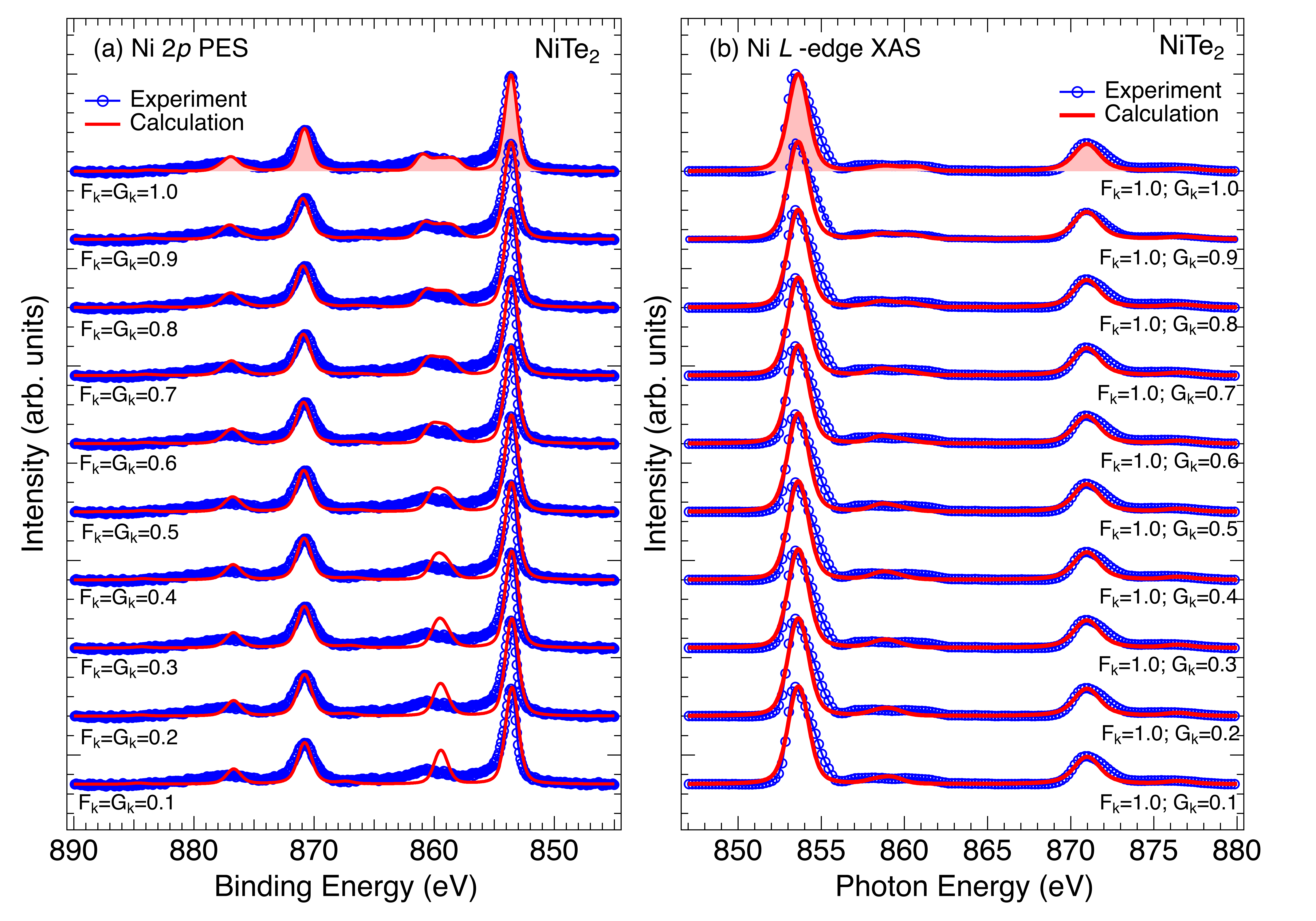
In Fig. 8(a) and (b), we plot a series of calculated Ni 2 PES and Ni -edge XAS spectra, respectively, in order to check the optimal value of Fk and Gk for NiTe2. By varying them together from a reduction factor of R = 1.0 to 0.1, keeping all other parameters fixed to the optimal values for NiTe2, we confirm that for R = 1.0 i.e. no reduction of Fk and Gk results in the least deviation compared to experiment.
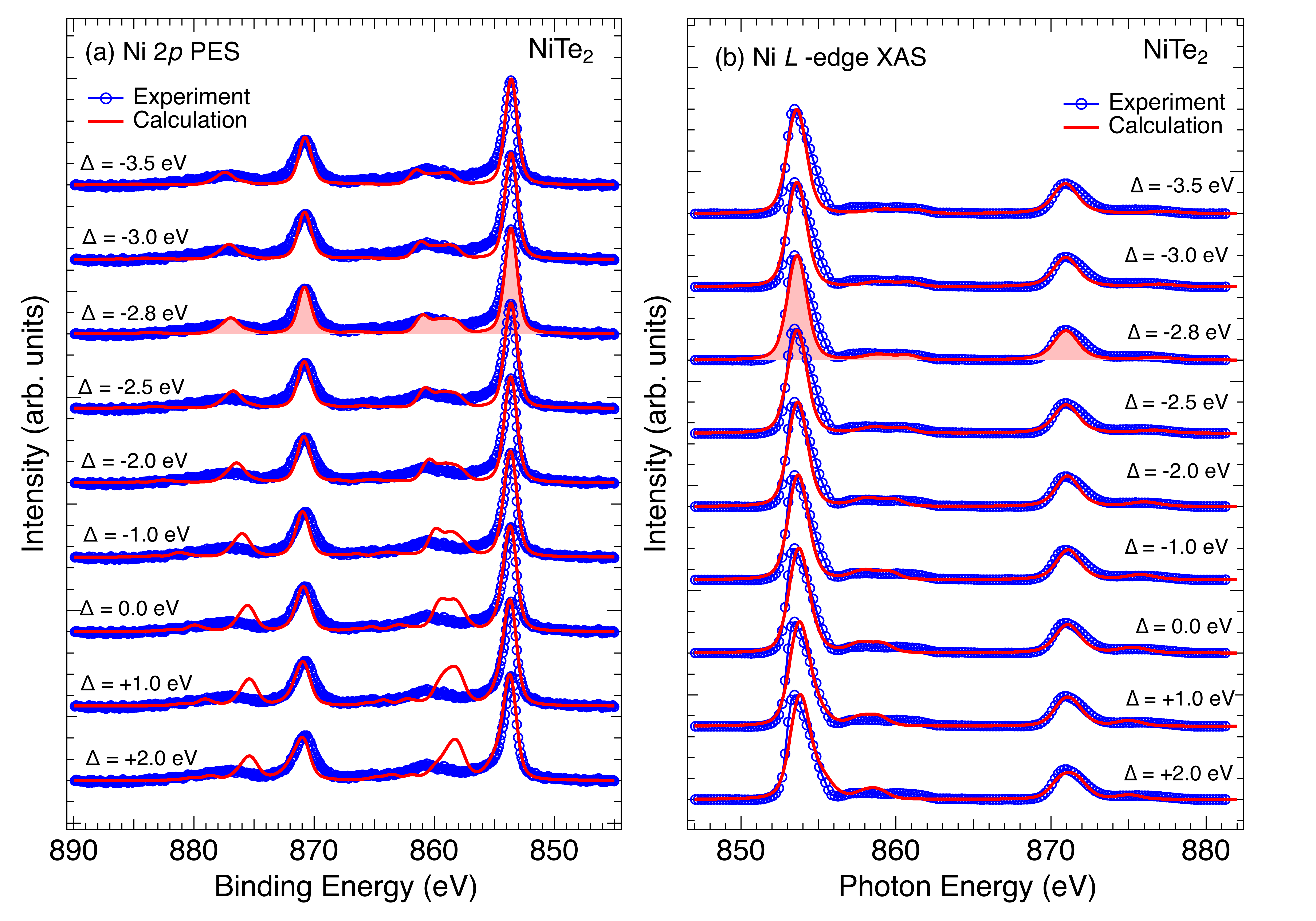
In Fig. 9(a) and (b), we plot a series of calculated Ni 2 PES and Ni -edge XAS spectra, respectively, to check the optimal value of charge transfer energy for NiTe2. By varying it from = -3.5 eV to +2.0 eV, and keeping all other parameters fixed to the optimal values, it is confirmed that the Ni 2 and Ni 2 PES satellites to the main peaks as well as the Ni -edge XAS satellites show the least deviation compared to the experiment for = -2.8 eV.
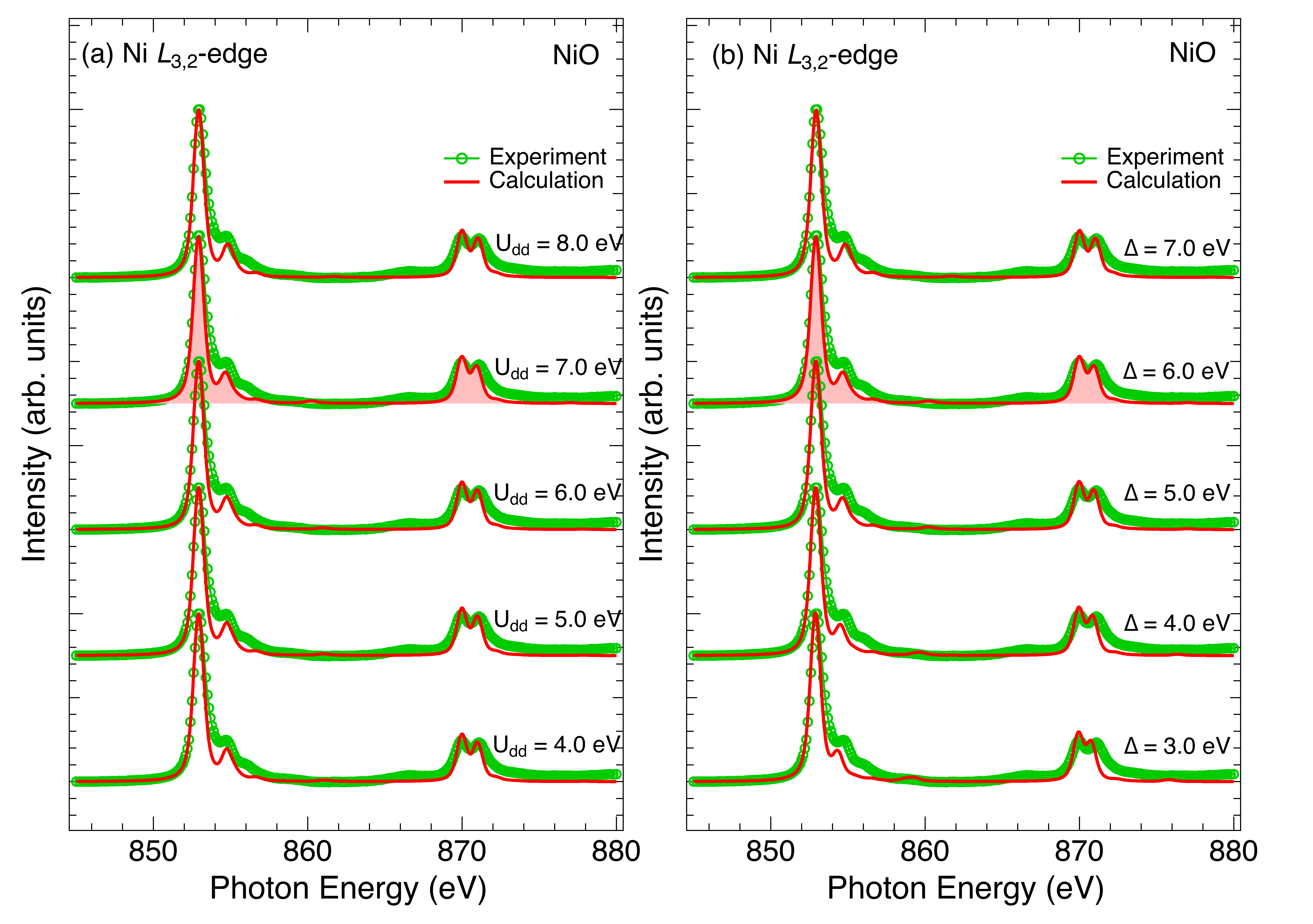
Figure 10 (a) and (b) shows a series of calculated Ni -edge XAS spectra for checking the the optimal value of on-site Coulomb energy and charge transfer energy for NiO, respectively. is varied from 4.0 eV to 8.0 eV, in 1.0 eV steps, by keepng all other parameter fixed (Fig. 10 (a)) and is varied from 3.0 eV to 7.0 eV, in 1.0 eV steps, by keeping all other parameters fixed (Fig. 10 (b)). The results confirm that the least deviation between calculated and experimental spectra is obtained for = 7.0 eV and = 6.0 eV.
References
- (1) M. König, S. Wiedmann, C. Brüne, A. Roth, H. Buhmann, L. W. Molenkamp, X.-L. Qi, and S.-C. Zhang, Quantum spin Hall insulator state in HgTe quantum wells, Science 318, 766 (2007)
- (2) D. Hsieh, D. Qian, L. Wray, Y. Xia, Y. S. Hor, R. J. Cava and M. Z. Hasan, A topological Dirac insulator in a quantum spin Hall phase. Nature 452, 970-974 (2008).
- (3) S. Murakami, N. Nagaosa, N. and S.-C. Zhang, Spin-Hall insulator, Phys. Rev. Lett. 93, 156804 (2004).
- (4) C. L. Kane and E. J. Mele, Z2 topological order and the quantum spin Hall effect, Phys. Rev. Lett. 95, 146802 (2005).
- (5) B. A. Bernevig, T. L. Hughes and S.-C. Zhang, Quantum spin Hall effect and topological phase transition in HgTe quantum wells, Science 314, 1757-1761 (2006).
- (6) C. L. Kane and E. J. Mele, Topological insulators in three dimensions, Phys. Rev. Lett. 98, 106803 (2007).
- (7) J. E. Moore and L. Balents, Topological invariants of time-reversal-invariant band structures, Phys. Rev. B 75, 121306(R) (2007).
- (8) R. Roy, Topological phases and the quantum spin Hall effect in three dimensions, Phys. Rev. B 79, 195322 (2009).
- (9) H. Zhang, C. -X. Liu, X. -L. Qi, X. Dai, Z. Fang and S. -C. Zhang, Topological insulators in Bi2Se3, Bi2Te3 and Sb2Te3 with a single Dirac cone on the surface, Nat. Phys. 5, 438 (2009).
- (10) B. A. Volkov and O. A. Pankratov, Two-dimensional massless electrons in an inverted contact, JETP Lett. 42, 178(1985).
- (11) O. A. Pankratov, S.V. Pakhomov and B.A. Volkov, Supersymmetry in heterojunctions: Band-inverting contact on the basis of Pb1-xSnTe and Hg1-xCdTe, Solid State Commun. 61, 93 (1987).
- (12) Y. Xia, D. Qian, D. Hsieh, L. Wray, A. Pal, H. Lin, A. Bansil, D. Grauer, Y. S. Hor, R. J. Cava and M. Z. Hasan, Observation of a large-gap topological-insulator class with a single Dirac cone on the surface, Nat. Phys. 5, 398 (2009).
- (13) Y. L. Chen, J. G. Analytis, J.-H. Chu, Z. K. Liu, S. -K. Mo, X. L. Qi, H. J. Zhang, D. H. Lu, X. Dai, Z. Fang, S. C. Zhang, I. R. Fisher, Z. Hussain, Z. -X. Shen, Experimental realization of a three-dimensional topological insulator, Bi2Te3, Science 325, 178 (2009).
- (14) D. Hsieh, Y. Xia, D. Qian, L. Wray, F. Meier, J. H. Dil, J. Osterwalder, L. Patthey, A. V. Fedorov, H. Lin, A. Bansil, D. Grauer, Y. S. Hor, R. J. Cava, and M. Z. Hasan, Observation of time-reversal-protected single-Dirac-cone topological-insulator states in Bi2Te3 and Sb2Te3, Phys. Rev. Lett. 103, 146401(2009).
- (15) A. A. Burkov and L. Balents, Weyl semimetal in a topological insulator multilayer, Phys. Rev. Lett. 107, 127205 (2011).
- (16) A. B. Sushkov, J. B. Hofmann, G. S. Jenkins, J. Ishikawa, S. Nakatsuji, S. Das Sarma, and H. D. Drew, Optical evidence for a Weyl semimetal state in pyrochlore Eu2Ir2O7, Phys. Rev. B 92, 241108(R) (2015).
- (17) B. Q. Lv, H. M. Weng, B. B. Fu, X. P. Wang, H. Miao, J. Ma, P. Richard, X. C. Huang, L. X. Zhao, G. F. Chen, Z. Fang, X. Dai, T. Qian, and H. Ding, Experimental discovery of Weyl semimetal TaAs, Phys. Rev. X 5, 031013 (2015).
- (18) S. -M. Huang, S. -Y. Xu, I. Belopolski, C. -C. Lee, G. Chang, B. Wang, N. Alidoust, G. Bian, M. Neupane, C. Zhang, S. Jia, A. Bansil, H. Lin, and M. Z. Hasan, A Weyl Fermion semimetal with surface Fermi arcs in the transition metal monopnictide TaAs class, Nat. Commun. 6, 7373 (2015).
- (19) S. Souma, Z. Wang, H. Kotaka, T. Sato, K. Nakayama, Y. Tanaka, H. Kimizuka, T. Takahashi, K. Yamauchi, T. Oguchi, K. Segawa, and Y. Ando, Direct observation of nonequivalent Fermi-arc states of opposite surfaces in the noncentrosymmetric Weyl semimetal NbP, Phys. Rev. B 93, 161112(R) (2016).
- (20) A. A. Zyuzin, Si Wu, and A. A. Burkov, Weyl semimetal with broken time reversal and inversion symmetries, Phys. Rev. B 85, 165110 (2012).
- (21) A. A. Burkov, Topological semimetals, Nat. Mater.15,1145 (2016).
- (22) M. S. Bahramy, O. J. Clark, B.-J. Yang, J. Feng, L. Bawden, J.M.Riley, I.Markovic, F.Mazzola, V.Sunko, D.Biswas, S. P. Cooil, M. Jorge, J. W. Wells, M. Leandersson, T. Balasubramanian, J. Fujii, I. Vobornik, J. E. Rault, T. K. Kim, M. Hoesch, K. Okawa, M. Asakawa, T. Sasagawa, T. Eknapakul, W. Meevasana, and P. D. C. King, Ubiquitous formation of bulk Dirac cones and topological surface states from a single orbital manifold in transition-metal dichalcogenides, Nature Mater. 17, 21 (2018).
- (23) J. Shi, Y. Huan, M. Xiao, M. Hong, X. Zhao, Y. Gao, F. Cui, P. Yang, S. J. Pennycook, J. Zhao, and Y. Zhang, Two-Dimensional Metallic NiTe2 with Ultrahigh Environmental Stability, Conductivity, and Electrocatalytic Activity, ACS Nano 14, 9011 (2020).
- (24) Q. Mao, Y. Zhang, Q. Chen, R. Li, X. Geng, J. Yang, H. Hao, M. Fang, Metallicity and Paramagnetism of Single-Crystalline NiTe and NiTe2 Phys. Stat. Solidi B 257, 1000224 (2020).
- (25) Z. Feng, J. Si, T. Li, H. Dong, C. Xu, J. Yang, Z. Zhang, K. Wang, H. Wu, Q. Hou, J. -J. Xing, S. Wan, S. Li, W. Deng, J. Feng, A. Pal, F. Chen, S. Hu, J.-Y. Ge, C. Dong, N. -C. Yeh, Evidences for pressure-induced two-phase superconductivity and mixed structures of NiTe2 and NiTe in type-II Dirac semimetal NiTe2-x (x = 0.38 0.09) single crystals, Mater. Today Phys. 17, 100339 (2021).
- (26) J. Oh, H. J. Park, A. Bala, H.-S. Kim, N. Liu, S. Choo, M. H. Lee, S. J. Kim, and S. Kim, Nickel telluride vertically aligned thin film by radio-frequency magnetron sputtering for hydrogen evolution reaction, APL Mater. 8, 121104 (2020).
- (27) C. He, J.-Z. Zhao, M. Du, L.-Z. Zhang, J.-Y. Zhang, K. Yang, N. F. Q. Yuan, A. Seliverstov, E. Janssens, J.-Y. Ge, and Z. Li, Coexistence of topological surface states and superconductivity in Dirac semimetal NiTe2. (accepted in Phys. Rev. Lett.); DOI: https://doi.org/10.1103/vpl7-n6bp, cond-mat arXiv:2503.01337.
- (28) Z. K. Liu, B. Zhou, Y. Zhang, Z. J. Wang, H. M. Weng, D. Prabhakaran, S.-K. Mo, Z. X. Shen, Z. Fang, X. Dai, Z. Hussain, and Y. L. Chen, Discovery of a three-dimensional topological Dirac semimetal, Na3Bi, Science 343, 864 (2014).
- (29) S.-Y. Xu, C. Liu, S. K. Kushwaha, R. Sankar, J. W. Krizan, I. Belopolski, M. Neupane, G. Bian, N. Alidoust, T.-R. Chang, H.-T. Jeng, C.-Y. Huang, W.-F. Tsai, H. Lin, P. P. Shibayev, F.-C. Chou, R. J. Cava, and M. Z. Hasan, Observation of Fermi arc surface states in a topological metal, Science 347, 294 (2015).
- (30) M. Neupane, S.-Y. Xu, R. Sankar, N. Alidoust, G. Bian, C. Liu, I. Belopolski, T.-R. Chang, H.-T. Jeng, H. Lin, A. Bansil, F. Chou, and M. Z. Hasan, Observation of a three-dimensional topological Dirac semimetal phase in high-mobility Cd3As2, Nat. Commun. 5, 3786 (2014).
- (31) S. Borisenko, Q. Gibson, D. Evtushinsky, V. Zabolotnyy, B. Büchner, and R. J. Cava, Experimental realization of a three-dimensional Dirac semimetal, Phys. Rev. Lett. 113, 027603 (2014).
- (32) K. Zhang, M. Yan, H. Zhang, H. Huang, M. Arita, Z. Sun, W. Duan, Y. Wu, and S. Zhou, Experimental evidence for Type-II Dirac semimetal in PtSe2, Phys. Rev. B 96, 125102 (2017).
- (33) H.-J. Noh, J. Jeong, E.-J. Cho, K. Kim, B. I. Min, and B.-G. Park, Experimental realization of type-II Dirac fermions in a PdTe2 superconductor, Phys. Rev. Lett. 119, 016401 (2017).
- (34) M. Yan, H. Huang, K. Zhang, E. Wang, W. Yao, K. Deng, G. Wan, H. Zhang, M. Arita, H. Yang, Z. Sun, H. Yao, Y. Wu, S. Fan, W. Duan, and S. Zhou, Lorentz-violating Type-II Dirac fermions in transition metal dichalcogenide PtTe2, Nat. Comm. 8, 257 (2017).
- (35) O. J. Clark, M. J. Neat, K. Okawa, L. Bawden, I. Markovic, F. Mazzola, J. Feng, V. Sunko, J. M. Riley, W. Meevasana, J. Fujii, I. Vobornik, T. K. Kim, M. Hoesch, T. Sasagawa, P. Wahl, M. S. Bahramy, and P. D. C. King, Fermiology and superconductivity of topological surface states in PdTe2, Phys. Rev. Lett. 120, 156401 (2018).
- (36) A. Chakraborty, J. Fujii, C.-N. Kuo, C. S. Lue, A. Politano, I. Vobornik, and A. Agarwal, Observation of highly anisotropic bulk dispersion and spin-polarized topological surface states in CoTe2, Phys. Rev. B 107, 085406 (2023).
- (37) C. Xu, B. Li, W. Jiao, W. Zhou, B. Qian, R. Sankar, N. D. Zhigadlo, Y. Qi, D. Qian, F.-C. Chou, and X. Xu, Topological Type-II Dirac fermions approaching the Fermi level in a transition metal dichalcogenide NiTe2, Chem. Mater. 30, 4823 (2018).
- (38) B. Ghosh, D. Mondal, C.-N. Kuo, C. S. Lue, J. Nayak, J. Fujii, I. Vobornik, A. Politano, and A. Agarwal, Observation of bulk states and spin-polarized topological surface states in transition metal dichalcogenide Dirac semimetal candidate NiTe2, Phys. Rev. B 100, 195134 (2019).
- (39) S. Mukherjee, S. W. Jung, S. F. Weber, C. Xu, D. Qian, X. Xu, P. K. Biswas, T. K. Kim, L. C. Chapon, M. D. Watson, J. B. Neaton, and C. Cacho, Fermi-crossing Type-II Dirac fermions and topological surface states in NiTe2, Sci. Rep. 10, 12957 (2020).
- (40) J. A. Hlevyack, L.-Y. Feng, M.-K. Lin, R. A. B. Villaos, R.-Y. Liu, P. Chen, Y. Li, S.-K. Mo, F.-C. Chuang, and T.-C. Chiang, Dimensional crossover and band topology evolution in ultrathin semimetallic NiTe2 films, npj 2D mater. appl 5, 40 (2021).
- (41) M. Nurmamat, S. V. Eremeev, X. Wang, T. Yoshikawa, T. Kono, M. Kakoki, T. Muro, Q. Jiang, Z. Sun, M. Ye, and A. Kimura, Bulk Dirac cone and highly anisotropic electronic structure of NiTe2, Phys. Rev. B 104, 155133 (2021).
- (42) F. Fischer, A. Torche, M. Prada, and G. Bester, GW effects on the topology of Type-II Dirac cones in NiTe2 , PtSe2 , and PtTe2, Phys. Rev. B 110, 165146 (2024).
- (43) N. Bhatt, A. Ali, D. Sharma, S. Bansal, M. Mandal, R. P. Singh and R. S. Singh, Strongly correlated topological surface states in the type-II Dirac semimetal NiTe2, Phys. Rev. B 111, 245157 (2025).
- (44) S. Jobic, R. Brec and J. Rouxel, Anionic polymeric bonds in transition metal ditellurides, J. Solid State Chem. 96, 169 (1992).
- (45) W. Bensch, W. Heid, M. Muhler, S. Jobic, R. Brec, and J. Rouxel, Anionic polymeric bonds in nickel ditelluride: crystal structure, and experimental and theoretical band structure, J. Solid State Chem. 121, 87 (1996).
- (46) W. Zheng, R. Schanemann, S. Mozaffari, Y. C. Chiu, Z. B. Goraum, N. Aryal, E. Manousakis, T. M. Siegrist, K. Wei, and L. Balicas, Bulk Fermi surfaces of the Dirac type-II semimetallic candidate NiTe2, Phys. Rev. B 102, 125103 (2020).
- (47) J. Zaanen, G. Sawatzky, and J. Allen, Band gaps and electronic structure of transition-metal compounds, Phys. Rev. Lett. 55, 418 (1985).
- (48) A. Prodan, F.W. Boswell., and J. M. Corbett, An electron microscopic investigation of CoTe2 Single Crystals, Phys. Stat. Sol.(a) 36, K21 (1976).
- (49) https://www.topologicalquantumchemistry.com/
- (50) M. W. Haverkort, M. Zwierzycki, and O. K. Andersen, Multiplet ligand-field theory using Wannier orbitals, Phys. Rev. B 85, 165113 (2012).
- (51) Y. Lu, M. Hoppner, O. Gunnarsson, and M. W. Haverkort, Efficient real-frequency solver for dynamical mean-field theory, Phys. Rev. B 90, 085102 (2014).
- (52) M. W. Haverkort, G. Sangiovanni, P. Hansmann, A. Toschi, Y. Lu, and S. Macke, Bands, resonances, edge singularities and excitons in core level spectroscopy investigated within the dynamical mean-field theory, EPL 108, 57004 (2014).
- (53) J. F. Moulder, W. F. Stickle, P. E. Sobol, and K. D. Bomben, Handbook of X-ray Photoelectron Spectroscopy (Perkin-Elmer Corporation, 1992).
- (54) A complementary study on experimental and cluster model analyses of negative charge transfer correlated metals is submitted to Phys. Rev. Lett.
- (55) S. Nappini, D. W. Boukhvalov, G. D’Olimpio, L. Zhang, B. Ghosh, C.-N. Kuo, H. Zhu, J. Cheng, M. Nardone, L. Ottaviano, et al., Transition-metal dichalcogenide NiTe2: An ambient-stable material for catalysis and nanoelectronics, Adv. Funct. Mater. 30, 2000915 (2020).
- (56) M. Trzhaskovskaya and V. Yarzhemsky, Dirac-Fock photoionization parameters for HAXPES applications, At. Data Nucl. Data Tables 119, 99 (2018).
- (57) M. Cini, Density of states of two interacting holes in a solid, Solid State Commun. 20, 605 (1976).
- (58) M. Cini, Two hole resonances in the XVV Auger spectra of solids, Solid State Commun. 24, 681 (1977).
- (59) G. Sawatzky, Quasiatomic Auger spectra in narrow-band metals, Phys. Rev. Lett. 39, 504 (1977).
- (60) P. Orders, J. Liesegang, R. Leckey, J. G. Jenkin, and J. Riley, Angle-resolved photoemission from the valence bands of NiTe2, PdTe2 and PtTe2, J. Phys. F: Met. Phys. 12, 2737 (1982).
- (61) C. Guillot, Y. Ballu, J. Paigne, J. Lecante, K. Jain, P. Thiry, R. Pinchaux, Y. Petroff, and L. Falicov, Resonant photoemission in nickel metal, Phys. Rev. Lett. 39, 1632 (1977).
- (62) M. Weinelt, A. Nilsson, M. Magnuson, T. Wiell, N. Wassdahl, O. Karis, A. Föhlisch, N. Mårtensson, J. Stöhr,, and M. Samant, Resonant photoemission at the 2 edges of Ni: Resonant Raman and interference effects, Phys. Rev. Lett. 78, 967 (1997).
- (63) S. Hüfner S.-H. Yang, B. Mun, C. Fadley, J. Schäfer, E. Rotenberg, and S. Kevan, Observation of the two-hole satellite in Cr and Fe metal by resonant photoemission at the 2 absorption energy, Phys. Rev. B 61, 12582 (2000).
- (64) P. Settembri, F. Mazzola, I. Vobornik, J. Fujii, M. Kögler, C.-N. Kuo, C. S. Lue, A. Politano, and G. Profeta, Unveiling strain-responsive topological landscapes in the NiTe2 Dirac semimetal, Phys. Rev. B 110, L201401 (2024).
- (65) M. A.Veenendaal, D. Alders and G. A. Sawatzky, Influence of superexchange on Ni 2p x-ray absorption spectroscopy in NiO, Phys. Rev. B 51, 13966 (1995).
- (66) D. Alders, L. Tjeng, F. Voogt, T. Hibma, G. Sawatzky, C. Chen, J. Vogel, M. Sacchi, and S. Iacobucci, Temperature and thickness dependence of magnetic moments in NiO epitaxial films, Phys. Rev. B 57, 11623 (1998).
- (67) A. Fujimori and F. Minami, Valence-band photoemission and optical absorption in nickel compounds, Phys. Rev. B 30, 957(1984).
- (68) M. A. van Veenendaal and G. A. Sawatzky, Nonlocal screening effects in 2p x-ray photoemission spectroscopy core-level line shapes of transition metal compounds, Phys. Rev. Lett. 70, 2459 (1993).
- (69) M. Ghiasi, A. Hariki, M. Winder, J. Kunes, A. Regoutz, T.-L. Lee, Y. Hu, J.-P. Rueff, and F. M. F. de Groot, Charge-transfer effect in hard x-ray 1s and 2p photoemission spectra: LDA +DMFT and cluster-model analysis, Phys. Rev. B 100, 075146(2019).