High Impedance Granular Aluminum Ring Resonators
Abstract
Superconducting inductors with impedance surpassing the resistance quantum, i.e., superinductors, are important for quantum technologies because they enable the development of protected qubits, enhance coupling to systems with small electric dipole moments, and facilitate the study of phase-slip physics. We demonstrate superinductors with densely packed meandered traces of granular aluminum (grAl) with inductances up to , achieving impedances exceeding in the range. Ring resonators made with grAl meandered superinductors exhibit quality factors on the order of in the single-photon regime, and low non-linearity on the order of tens of Hz. Depending on the grAl resistivity, at , we measure frequency noise spectral densities in the range of to . In some devices, in the single-photon regime, we observe a positive Kerr coefficient of unknown origin. Using more complex fabrication, the devices could be released from the substrate, either freestanding or suspended on a membrane, thereby further improving their impedance by a factor of three.
In circuits with high characteristic impedance , zero-point voltage fluctuations are enhanced [1, 2], , enabling coupling of superconducting microwave devices to other systems, e.g. phonons via direct piezoelectric coupling [3] or parametric electromechanical interactions [4], molecular qubits [5], as well as small electric dipoles and spins in quantum dots [2]. At the high end of , inductors with zero DC resistance and impedance exceeding the resistance quantum, , are known as superinductors [6, 7]. They enable the realization of protected qubit architectures, such as fluxonium [8, 9, 10, 11, 12, 13, 14] and qubits [15, 16, 17], by delocalizing the wavefunction and mitigating flux noise. The high inductive reactance of superinductors is also essential for studying flux-tunneling-induced phase slips, facilitating the observation of dual Shapiro steps [18, 19, 20].
Long Josephson junction arrays are a widely used option for achieving high-impedance with low-loss [6, 7], and their impedance can exceed hundreds of when suspended in vacuum [21, 22]. However, these arrays—particularly in suspended configurations—are complex to fabricate and introduce unwanted non-linearity [23]. Alternatively, geometric inductors optimized into suspended spiral shapes offer high linearity but remain challenging to fabricate [24, 25].
An ideal superinductor technology would combine low dissipation, straightforward fabrication, and compatibility across diverse operational environments, including high magnetic fields, as required for example in spin [2], Andreev [26], or nanowire qubit devices [27, 28, 29].
In this context, disordered superconductors are particularly attractive because they can be densely patterned using standard lithographic techniques, while contributing substantial kinetic inductance dominating the total inductive response. Among the various candidate materials, several have been employed to fabricate devices exhibiting characteristic impedance higher than and internal quality factors above in the single-photon regime. These include NbN [30, 31, 23], TiN [32, 33, 34], NbTiN [35, 36, 37], NbAlN [38], and grAl [39, 10, 40, 41, 42]. The associated self-Kerr non-linearity can be tuned from approximately to for both NbN [23, 43] and TiN [44], and from to for granular aluminum (grAl) [45, 46]. In a recent study [47], the authors compare NbN and grAl devices, highlighting the following trade-off: NbN offers superior magnetic-field resilience, beneficial for hybrid circuit quantum electrodynamics, while grAl is better suited to low-field regimes requiring high impedance and strong non-linearity.
Here, we utilize grAl to explore the high-impedance frontier with meandered trace ring resonators. The meandering design is practical for achieving high-impedance as it allows for long inductive lines within a small area, maximizing inductance while minimizing capacitance [40]. We demonstrate ring resonators with impedance above in the technologically relevant frequency range of . These resonators achieve quality factors around in the single-photon regime, with non-linearity in the tens of . Frequency noise spectral densities at range from to , depending on grAl resistivity.
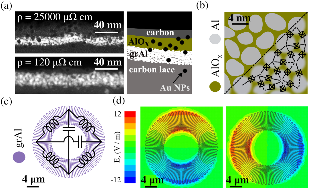
GrAl is a nanocomposite of \ceAl grains in an aluminum oxide matrix (see Fig. 1(a)), forming a self-assembled 3D network of Josephson junctions (see Fig. 1(b)). It is superconducting for a wide range of normal state resistivities ranging from 1 to [48], which can be adjusted via the oxygen partial pressure during deposition. This tunability enables precise control over its kinetic inductance allowing the realization of inductors predominantly governed by kinetic inductance, with a kinetic inductance fraction approaching unity, where is the geometric inductance.
where is the kinetic inductance per square, is the Boltzmann constant, is the superconducting critical temperature, and is the normal-state sheet resistance. The superconducting gap is linked to the critical temperature by with for grAl resistivity below and for the high resistivity range [52, 48].
In order to increase the characteristic impedance of the resonator , where and is the resonator’s total capacitance, it is essential to optimize the resonator design to minimize and maximize . This is achieved by employing a meandered ring resonator (see Fig. 1(c)), where the capacitance is reduced by decreasing the ring’s outer radius and using the smallest possible meander pitch . Since is close to unity, is predominantly enhanced by increasing the kinetic inductance through two mechanisms: increasing the number of squares in the trace, by increasing the length and reducing the width of the resonator, and raising the sheet resistance , which can be achieved by using higher-resistivity films and by reducing film thickness.
As shown in Fig. 1(d), when the ring is closed, the symmetric design of this distributed resonator results in two fundamental modes. The effective circuit model for each mode comprises a capacitor shunted by two parallel inductors .
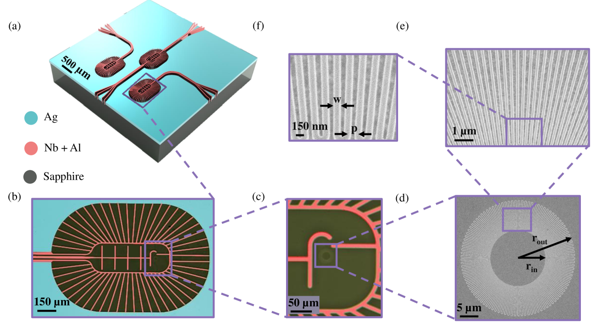
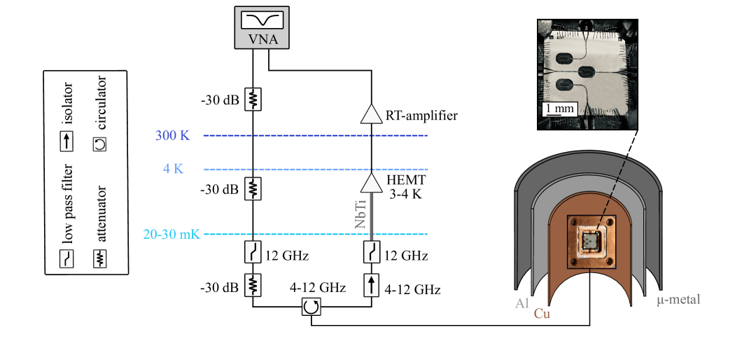
The resonators are capacitively coupled to a common coplanar waveguide (CPW) for reflection measurements, as shown in Fig. 2. The entire structure is integrated within a silver ground plane, which suppresses parasitic modes and ensures a uniform magnetic field across the chip. Near the end of each CPW we push the normal ground plane away from the central pin, in order to reduce dissipation. In the proximity of the devices, the ground plane consists of narrow superconducting lines connected to the normal plane, which avoid the creation of superconducting loops and associated flux trapping. The configuration of the end of CPW feed line enables flexible coupling to the small rings. It intentionally creates different coupling strengths for the two modes, thereby breaking the symmetry and lifting the degeneracy of the two fundamental modes. Positioning the ring near the semicircular structure at the end of the feed line (see Fig. 2(c)) results in strong coupling for both modes, while placing it within a square structure visible in the center of Fig. 2(b) leads to uneven coupling of the modes to the feed line. The compact design allows for the integration of three separate CPW sets on a single chip, each isolated by the ground plane, enabling the measurement of multiple ring resonators with varying design parameters.
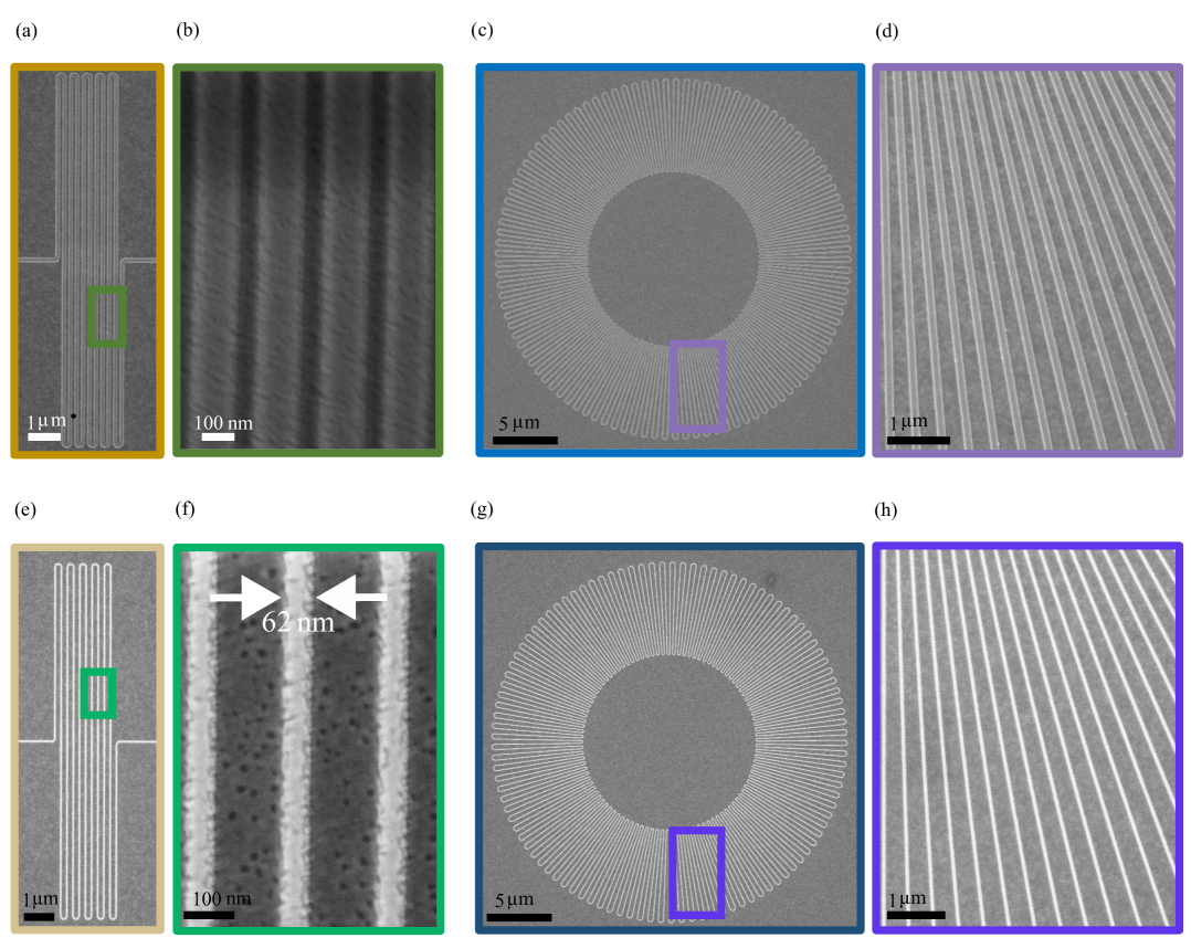
The rings are patterned using a single-step electron beam lithography process followed by lift-off on a c-plane sapphire substrate with zero-angle evaporation deposition. See Figs. 2(d-f) for images of one of the fabricated rings. The pitch values range from , with widths between 150 and , and film thicknesses from 20 to . We wire-bond each chip to a copper housing that is surrounded by magnetic and infrared radiation shielding barrels made of copper/aluminum and \cemu-metal (see Appendix A). The assembly is connected to the mixing chamber (MXC) stage of a dilution cryostat, operating at .
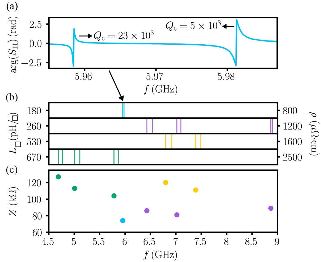
In Fig. 3(a), we show a typical phase response of a ring resonator in a microwave reflection measurement. The two fundamental modes are clearly visible, separated by approximately , with their respective coupling quality factors differing by approximately a factor of four.
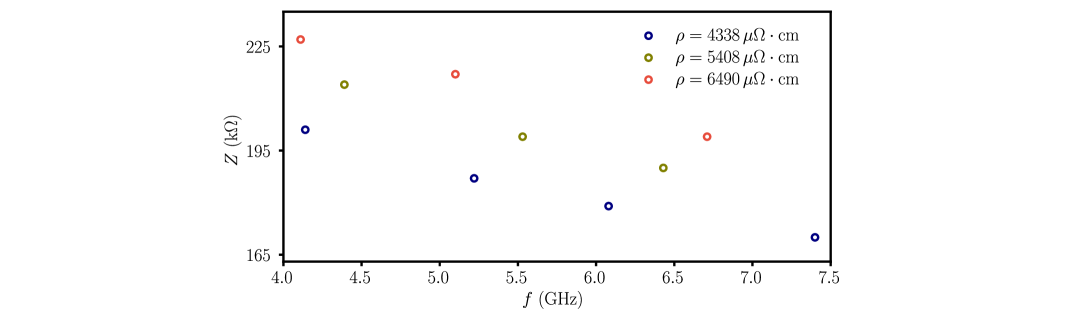
A summary of the measured fundamental modes frequencies for nine resonators is shown in Fig. 3(b), for grAl resistivities between and . By performing finite element simulations for rings with varying and matching the simulated frequencies with measurements, we deduce the inductance per square for each grAl film, ranging from 180 to 670 ().
We determine the impedance up to the first fundamental mode from the equation , where denotes the inductance of the entire ring [24, 21], as summarized in Fig 3(c). The highest impedance, , was achieved for a ring with a sheet inductance of , and specific dimensions of pitch , , , and thickness . A detailed summary of all measured devices is provided in Table 1 in Appendix B.
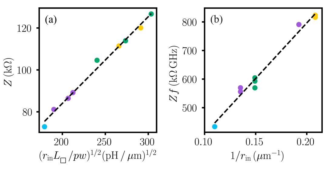
In a simplified model (see Appendix C), we find that the impedance and lowest mode frequency scale with the layout parameters and sheet inductance as follows:
| (2) |
Indeed, as shown in Fig. 4(a), the impedance for our measured resonators follows this scaling. Notice that , as illustrated in Fig. 4(b), which means that in order to maximize the impedance at a given frequency, we need to minimize and compensate the resulting change in frequency by decreasing the ratio . The lowest achievable value for the ratio depends on the grAl material properties and the finesse of the lithography. The maximum value for is limited by the resistivity threshold for the grAl superconducting-to-insulating transition [52, 48], in the range of , and by the thinnest continuous and stable films. For grAl films below we observe significant fluctuations in their resistivity between different cooldowns, indicating that structural inhomogeneities and instabilities play a dominant role. We found that devices with always resulted in stable devices, which was not the case for , likely due to inhomogeneities in the wires (see Fig. 1(a)). The smallest pitch we could achieve with our current electron-beam lithography was (see Appendix D). Taking these considerations into account, we believe that a fine-tuned optimal grAl device operational in the 4-8 range can reach impedance values in the range of (see Appendix E) on Silicon or Sapphire substrates, and this value can be increased by a factor of , to exceed for suspended devices.
We calculate the noise spectral density by monitoring the resonant frequency over time and applying the method used in [55]. As shown in Fig. 5(a), the low-frequency noise exhibits a dependence. We note that evaluated at a frequency of is observed in the range of , which is one to two orders of magnitude larger than for grAl resonators of similar thickness and resistivity, but lower impedance [56]. In addition, these values are two orders of magnitude larger compared to aluminum resonators [57]. The frequency-independent noise component at high-frequency (white noise), modeled by a constant amplitude , is due to the measurement setup. It is nearly negligible in our data. To model the low-frequency noise, we use , where . Fitting this model to the measurements shown in Fig. 5(a), ranges from to , which could be due to contributions from other noise sources. Note that the three data sets with the highest resistivity exhibit visible deviations from pure dependence, which is compatible with an added Lorentzian component. This suggests the presence of random telegraph noise, which decays exponentially over a characteristic timescale given by the position of the peak in the noise spectrum[58]. Note that in our case, the peak is less pronounced than in Ref. [59].
To evaluate loss in the resonators, we measure the complex signal and extract the internal quality factor and the coupling quality factor using the method in Ref. [60]. To minimize Fano interference systematic errors, we design comparable to . In Fig. 5(b) we plot the fitted values as a function of photon number . In the single-photon regime, is on the order of and appears independent of resistivity and impedance. The value aligns with previous results for granular aluminum resonators made using similar processes [61]. Since the participation ratio in the compact resonators presented here is larger, this suggests that, within the explored range, surface dielectric losses are not dominant. Recently, in reference [42] it was demonstrated that by optimizing fabrication and using thicker layers at similar resistivities, but lower impedance, quality factors above can be achieved. These low levels of loss make high-impedance grAl resonators appealing for superconducting quantum circuits. At higher power levels, saturates to values close to , indicating that the dominant loss mechanism, potentially dielectric loss [62, 63] or quasiparticle bursts [64, 65], is saturable, as commonly observed for other superconducting materials.
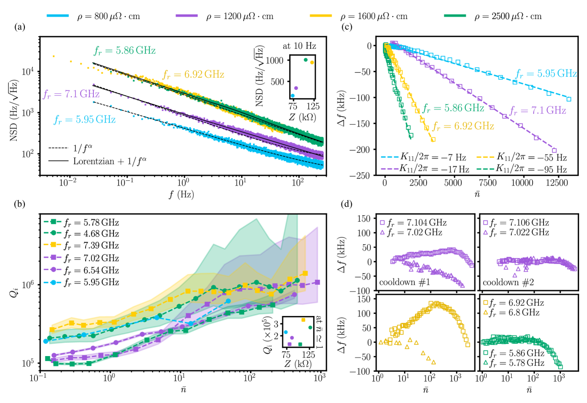
In Fig. 5(c) we show that the resonators are comparatively linear, considering their high-impedance. We determine the Kerr coefficient , which quantifies the frequency shift of the fundamental mode with the addition of one photon, by performing a linear fit to the frequency shift as a function of in the high-photon-number regime. Our measurements indicate that is in the range of tens of . As can be seen in Fig. 5(c), resonators with higher resistivity and thinner films exhibit larger values compared to those with lower resistivity and thicker films. This is consistent with modeling grAl as a 1D array of Josephson junctions [45], in that case we expect , where is the resonator current mode volume.
An intriguing aspect of our measurements is the observation of a positive frequency shift as a function of photon number in some resonators, as shown in Fig. 5(d). We observe that the frequency initially increases at very low photon numbers before the drop corresponding to the Kerr non-linearity discussed in the previous paragraph. Some ring resonators exhibit this effect, while others do not, and we could not identify a correlation of this effect with resistivity, impedance, or other device parameters. Additionally, this positive frequency shift vs. can vary for the same device in-between cooldowns. Similar observations have recently been reported on resonators integrating a flake of van der Waals cuprate superconductor [66]. This behavior is highly relevant for quantum devices operating in the low-power regime, and it needs further investigation to fully understand its underlying mechanisms, possibly related to strongly coupled spurious two-level systems [67, 68, 69].
In summary, we fabricated and characterized granular aluminum meandered trace ring resonators, achieving high-impedance with a single-step lift-off e-beam lithography process. We propose a model in which the impedance and frequency of grAl resonators scale predictably with design parameters, with maximal impedance achieved by minimizing the diameter and correspondingly adjusting the pitch, trace-width and sheet inductance, within material and lithographic constraints. Our best devices exhibit kinetic inductances up to and impedances exceeding , about 16 times the resistance quantum. We demonstrated quality factors on the order of in the single-photon regime, making them suitable for quantum information processing. Their measured self-Kerr non-linearity, in the range of tens of , is significantly lower than in Josephson junction arrays. Interestingly, we observe an anomalous positive frequency shift at low photon numbers of unknown origin. Further impedance enhancements could be achieved by reducing the dielectric constant, for example, through backside etching or by detaching from the substrate.
Acknowledgements
We are grateful to L. Radtke and S. Diewald for technical assistance. We thank Mathieu Fechant, Horst Hahn, David Niepce, Dennis Rieger, and Patrick Winkel for constructive discussions and feedback. We acknowledge funding from the European Union’s Horizon 2020 research and innovation program under the Marie Skłodowska-Curie grant agreement number 847471 (QUSTEC) and the Federal Ministry of Education and Research (Projects QSolid (FKZ:13N16151) and GeQCoS (FKZ: 13N15683)). Facilities use was supported by the KIT Nanostructure Service Laboratory (NSL) and by the Karlsruhe Nano Micro Facility (KNMFi). We acknowledge qKit for providing a convenient measurement software framework.
Appendix A Setup
As shown in Fig. 6, each chip’s CPW is aluminum wire-bonded to a transmission line, with the ground plane bonded to a non-magnetic, oxygen-free, high-conductivity copper box to minimize spurious modes. This box features a tightly screwed lid to prevent radiation leakage. The entire assembly is mounted on a copper rod attached to the MXC stage of a dilution cryostat and enclosed within a series of magnetic shields similar to the setup in [54], including a \ceCu/\ceAl bilayer and an additional \ceMu-metal shield to ensure effective magnetic shielding.
The input signal, generated by a vector network analyzer (VNA), is transmitted through cables, with attenuators at various cryogenic stages as detailed in Fig. 6. For single-port reflection measurements, a cryogenic circulator separates the input and output signals. The reflected output signal then passes through a two-stage isolator, which shields against 4K stage radiation, and through a low-pass filter before reaching a low-noise high electron mobility transistor (HEMT) amplifier via \ceNbTi cables with minimal noise contribution. Finally, the amplified signal is sent to commercial room-temperature amplifiers and then back to the VNA output.
Appendix B Designed and Empirically Extracted Parameters
We confirmed the accuracy of geometric parameters via SEM imaging. The resonance frequency was measured experimentally as detailed in App. A. was determined by fitting the measured to simulated frequencies based on the nominal design parameters.
The total inductance was calculated based on the geometric parameters and , using the formula , where represents the number of squares. was calculated using Eqs. 1, with the critical temperature set approximately to 2.2 K for the calculation.
was derived from , assuming that the entire ring behaves as an inductor up to the resonance frequency. and were both extracted using the circle fit method. The value of is influenced by the ring’s position relative to the feed line, as well as the ring’s radius—the smaller the radius, the weaker the coupling.
A summary of all parameters discussed above is given in Table 1.
| Resonator | |||||||||||
| () | () | () | () | () | () | (/ | () | (fF) | () | ||
| 1 | 9.1 | 170 | 1849 | 300 | 30 | 5.95 | 180 | 1.95 | 1.46 | 72.9 | 23 |
| 2 | 9.1 | 170 | 1849 | 300 | 30 | 5.98 | 180 | 1.95 | 1.45 | 72.9 | 5 |
| 3 | 7.4 | 150 | 1239 | 300 | 30 | 6.43 | 260 | 2.14 | 1.14 | 86.45 | 5 |
| 4 | 7.4 | 150 | 1239 | 300 | 30 | 6.54 | 260 | 2.14 | 1.10 | 86.45 | 600 |
| 5 | 7.4 | 150 | 1066 | 355 | 30 | 7.02 | 260 | 1.84 | 1.11 | 81.15 | 150 |
| 6 | 7.4 | 150 | 1066 | 355 | 30 | 7.10 | 260 | 1.84 | 1.09 | 81.15 | 20 |
| 7 | 5.2 | 150 | 928 | 200 | 30 | 8.87 | 260 | 1.60 | 0.80 | 89.17 | 25 |
| 8 | 5.2 | 150 | 928 | 200 | 30 | 8.9 | 260 | 1.60 | 0.79 | 89.17 | 22 |
| 9 | 4.8 | 150 | 796 | 200 | 20 | 6.80 | 530 | 2.81 | 0.78 | 120.05 | 50 |
| 10 | 4.8 | 150 | 796 | 200 | 20 | 6.92 | 530 | 2.81 | 0.75 | 120.05 | 30 |
| 11 | 4.8 | 150 | 681 | 240 | 20 | 7.39 | 530 | 2.40 | 0.77 | 111.43 | 230 |
| 12 | 4.8 | 150 | 681 | 240 | 20 | 7.49 | 530 | 2.40 | 0.75 | 111.43 | 130 |
| 13 | 5.6 | 150 | 875 | 300 | 20 | 5.70 | 600 | 3.50 | 0.89 | 125.35 | 200 |
| 14 | 5.6 | 150 | 875 | 300 | 20 | 5.81 | 600 | 3.50 | 0.85 | 125.35 | 130 |
| 15 | 5.6 | 150 | 741 | 253 | 20 | 6.03 | 600 | 2.96 | 0.94 | 112.14 | 60 |
| 16 | 5.6 | 150 | 741 | 253 | 20 | 6.13 | 600 | 2.96 | 0.91 | 112.14 | 6 |
| 17 | 6.7 | 150 | 966 | 325 | 20 | 4.68 | 670 | 4.31 | 1.07 | 126.7 | 140 |
| 18 | 6.7 | 150 | 966 | 325 | 20 | 4.76 | 670 | 4.31 | 1.03 | 126.7 | 50 |
| 19 | 6.7 | 150 | 806 | 400 | 20 | 5.00 | 670 | 3.60 | 1.12 | 113.9 | 8 |
| 20 | 6.7 | 150 | 806 | 400 | 20 | 5.11 | 670 | 3.60 | 1.07 | 113.09 | 6 |
| 21 | 6.7 | 150 | 646 | 518 | 20 | 5.78 | 670 | 2.88 | 1.05 | 104.59 | 260 |
| 22 | 6.7 | 150 | 646 | 518 | 20 | 5.86 | 670 | 2.88 | 1.02 | 104.59 | 30 |
Appendix C Model of Ring Superinductors
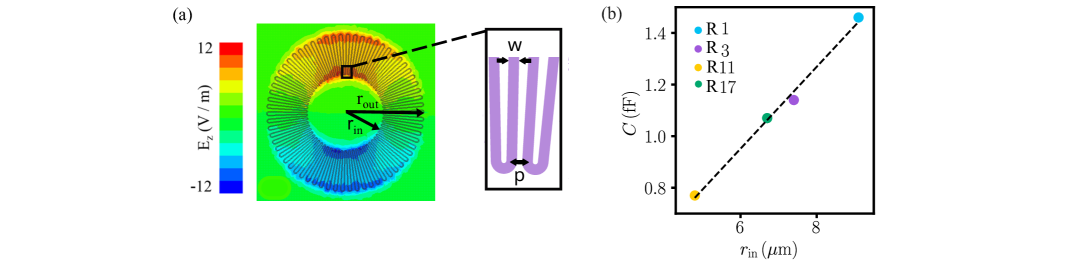
Ignoring the turns, which are approximately equal to the sum of and , the inductance can be approximated with the expression . As we can see in Fig. 7(a), is the wire width, is the inductance per square, and is the inner radius of the ring. The outer radius is related to the inner radius as: Here, is the number of meanders, which is proportional to , where is the pitch (the sum of wire width and spacing). Substituting this relationship, we find:
The capacitance of the ring resembles that of a coplanar capacitor composed of two square plates with sides and separated by a length . The capacitance of such a capacitor scales linearly with the plate width and thus . Therefore we can approximate the ring capacitance by [70].
In Fig. 7(b) we confirmed that this linear dependency is consistent with the capacitances determined from HFSS.
The resonance frequency is derived from the two expressions for and using the harmonic oscillator equation:
The impedance depends on both the inductance and capacitance of the ring and can be expressed again using the expressions for and determined above:
Again, we confirm this proportionality of to the design parameters for the resonators listed in Tab. 1 in the plot shown in Fig. 4(a). In addition, we confirm in Fig. 4(b) that the product only depends on the ring radius. This shows that, for a given fixed frequency, the impedance can be increased (maximizing the product) only by reducing the radius and compensating the associated frequency shift with one of the other design parameters ( ). This compensation does not affect the product .
Appendix D Fabrication
Device under test includes the ring resonators, CPW, and ground plane, is fabricated on a double-polished, 2 inches c-plane sapphire wafer with a thickness of . The lift-off lithography process (Details in Table 2) begins with spin coating a PMMA resist layer, followed by the application of a conductive coating. The resonators are patterned using a e-beam lithography system, followed by the removal of the conductive layer and the development of the resist pattern.
Subsequently, the wafer is transferred to a UHV Plassys e-beam evaporator, where it undergoes plasma cleaning, an \ceAr/O2 descum process. Titanium is then evaporated as a getter material to improve vacuum conditions, with the shutter kept closed during this step. The grAl layer is deposited at room temperature using e-beam evaporation of pure aluminum while flowing a small amount of oxygen through the chamber. After deposition, the grAl film is lifted off by dissolving the resist underneath it. The resistivity of the resulting grAl films ranges from to as determined by comparing the frequencies extracted from HFSS simulation with the measured ones, SEM images of representative devices are shown in Fig. 8.
Fabrication of the CPW starts with resist spin coating, UV lithography patterning, and development. The CPW metallization involves \ceAl + Nb deposition using the Plassys evaporator, including \ceAr/O2 descum cleaning and \ceTi gettering, followed by lift-off.
After the CPW lift-off process, an additional optical lithography step is performed to deposit the silver ground plane. This step mirrors the CPW fabrication process but includes an additional \ceAr cleaning step to remove any oxide layer on the \ceAl, ensuring good galvanic contact between the overlapping silver and \ceNb + Al structures, which is crucial for avoiding parasitic modes. (Fabrication steps in table 3)
After completing the patterning, a protective photoresist layer is applied, and the chip is diced into pieces of by . The final step involves cleaning off the protective resist layer.
| Resist Coating | |
| Substrate | C-plane sapphire |
| E-beam resist |
PMMA A4
(thickness = ) |
| Acceleration | |
| Spread cycle | for |
| Spin speed | for |
| Baking temperature | for |
| Conductive coating | Electra 92 (AR-PC 5090) |
| Acceleration | |
| Spread cycle | for |
| Spin speed | for |
| Baking temperature | for |
| E-beam Exposure | |
| Acceleration voltage | |
| Beam current | |
| Step size | |
| Development | |
| Conductive coating removal | Water (RT) for |
| Developer |
MIBK 1:3 IPA
at for |
| Deposition Process | |
| Plasma Cleaning | |
| Mass flows | \ceO2/\ceAr (/) |
| Beam parameters |
|
| Gettering | |
| Ti evaporation rate | for |
| grAl Deposition | |
| Al evaporation rate | |
| \ceO2 pressure | to |
| Resist Coating | |
| Substrate | C-plane sapphire |
| Photoresist | AZ 5214E |
| Acceleration | |
| Spin speed | for |
| Baking temperature | for |
| UV Exposure | |
| 1st Exposure | |
| Exposure power | for |
| Baking | |
| Baking temperature | for |
| 2nd Exposure | |
| Exposure type | Flood exposure for |
| Development | |
| Developer |
AZ developer 3:2 water
for |
| Deposition Process | |
| Plasma Cleaning | |
| Mass flows | \ceO2/\ceAr (/) |
| Beam parameters |
|
| Gettering | |
| \ceTi evaporation rate | for |
| \ceNb + \ceAl Deposition | |
| \ceNb evaporation rate | |
| Al evaporation rate | |
| \ceAg Deposition | |
| \ceAg evaporation rate | |
Appendix E Numerical Simulation of High-Resistivity Ring Resonators
To explore the higher resistivity regime of grAl below the superconducting-to-insulator phase transition (SIT), we simulated grAl ring resonators with ranging from to which could be achieved by using from to . These simulations are performed using the eigenmode solver in ANSYS HFSS to determine intrinsic resonant frequencies.
The simulated parameters, including resonator dimensions, inductance, resonance frequencies, and corresponding impedances, are presented in Table 4 and the impedance values are reported in Fig. 9, providing a perspective for future impedance increases in grAl resonators.
| Resonator | ||||||||||
| () | () | () | () | () | () | (/) | () | (fF) | () | |
| 23 | 3.2 | 120 | 367 | 200 | 20 | 7.3 | 1200 | 3.67 | 0.518 | 170 |
| 24 | 3.69 | 120 | 469.8 | 200 | 20 | 6.07 | 1200 | 4.69 | 0.586 | 179 |
| 25 | 4.07 | 120 | 571.9 | 200 | 20 | 5.22 | 1200 | 5.71 | 0.651 | 187 |
| 26 | 4.77 | 120 | 775.7 | 200 | 20 | 4.14 | 1200 | 7.75 | 0.763 | 201 |
| 27 | 3.31 | 120 | 377 | 200 | 20 | 6.43 | 1500 | 4.7 | 0.521 | 190 |
| 28 | 3.62 | 120 | 459 | 200 | 20 | 5.53 | 1500 | 5.7 | 0.581 | 199 |
| 29 | 4.2 | 120 | 622 | 200 | 20 | 4.39 | 1500 | 7.7 | 0.683 | 214 |
| 30 | 2.9 | 120 | 316 | 200 | 20 | 6.7 | 1800 | 4.7 | 0.480 | 199 |
| 31 | 3.6 | 120 | 452 | 200 | 20 | 5.09 | 1800 | 6.7 | 0.584 | 217 |
| 32 | 4.13 | 120 | 588 | 200 | 20 | 4.1 | 1800 | 8.8 | 0.685 | 227 |
References
- Devoret et al. [2007] M. Devoret, S. Girvin, and R. Schoelkopf, Circuit-QED: How strong can the coupling between a josephson junction atom and a transmission line resonator Be?, Ann. Phys. 519, 767 (2007).
- Burkard et al. [2023] G. Burkard, T. D. Ladd, A. Pan, J. M. Nichol, and J. R. Petta, Semiconductor spin qubits, Rev. Mod. Phys. 95, 025003 (2023).
- Arrangoiz-Arriola et al. [2018] P. Arrangoiz-Arriola, E. A. Wollack, M. Pechal, J. D. Witmer, J. T. Hill, and A. H. Safavi-Naeini, Coupling a superconducting quantum circuit to a phononic crystal defect cavity, Phys. Rev. X 8, 031007 (2018).
- Bozkurt et al. [2023] A. Bozkurt, H. Zhao, C. Joshi, H. G. LeDuc, P. K. Day, and M. Mirhosseini, A quantum electromechanical interface for long-lived phonons, Nat. Phys. 19, 1326 (2023).
- André et al. [2006] A. André, D. DeMille, J. M. Doyle, M. D. Lukin, S. E. Maxwell, P. Rabl, R. J. Schoelkopf, and P. Zoller, A coherent all-electrical interface between polar molecules and mesoscopic superconducting resonators, Nat. Phys. 2, 636 (2006).
- Manucharyan et al. [2012] V. E. Manucharyan, N. A. Masluk, A. Kamal, J. Koch, L. I. Glazman, and M. H. Devoret, Evidence for coherent quantum phase slips across a Josephson junction array, Phys. Rev. B 85, 024521 (2012).
- Masluk et al. [2012] N. A. Masluk, I. M. Pop, A. Kamal, Z. K. Minev, and M. H. Devoret, Microwave characterization of josephson junction arrays: Implementing a low loss superinductance, Phys. Rev. Lett. 109, 137002 (2012).
- Manucharyan et al. [2009] V. E. Manucharyan, J. Koch, L. I. Glazman, and M. H. Devoret, Fluxonium: Single cooper-pair circuit free of charge offsets, Science 326, 113 (2009).
- Pop et al. [2014] I. M. Pop, K. Geerlings, G. Catelani, R. J. Schoelkopf, L. I. Glazman, and M. H. Devoret, Coherent suppression of electromagnetic dissipation due to superconducting quasiparticles, Nature 508, 369 (2014).
- Grünhaupt et al. [2019] L. Grünhaupt, M. Spiecker, D. Gusenkova, N. Maleeva, S. T. Skacel, I. Takmakov, F. Valenti, P. Winkel, H. Rotzinger, W. Wernsdorfer, A. V. Ustinov, and I. M. Pop, Granular aluminium as a superconducting material for high-impedance quantum circuits, Nat. Mater. 18, 816 (2019).
- Pita-Vidal et al. [2020] M. Pita-Vidal, A. Bargerbos, C.-K. Yang, D. J. Van Woerkom, W. Pfaff, N. Haider, P. Krogstrup, L. P. Kouwenhoven, G. De Lange, and A. Kou, Gate-tunable field-compatible fluxonium, Phys. Rev. Appl. 14, 064038 (2020).
- Nguyen et al. [2022] L. B. Nguyen, G. Koolstra, Y. Kim, A. Morvan, T. Chistolini, S. Singh, K. N. Nesterov, C. Jünger, L. Chen, Z. Pedramrazi, B. K. Mitchell, J. M. Kreikebaum, S. Puri, D. I. Santiago, and I. Siddiqi, Blueprint for a high-performance fluxonium quantum processor, PRX Quantum 3, 037001 (2022).
- Peruzzo et al. [2021] M. Peruzzo, F. Hassani, G. Szep, A. Trioni, E. Redchenko, M. Žemlička, and J. M. Fink, Geometric superinductance qubits: Controlling phase delocalization across a single josephson junction, PRX Quantum 2, 040341 (2021).
- Kalashnikov et al. [2020] K. Kalashnikov, W. T. Hsieh, W. Zhang, W.-S. Lu, P. Kamenov, A. Di Paolo, A. Blais, M. E. Gershenson, and M. Bell, Bifluxon: Fluxon-parity-protected superconducting qubit, PRX Quantum 1, 010307 (2020).
- Brooks et al. [2013] P. Brooks, A. Kitaev, and J. Preskill, Protected gates for superconducting qubits, Phys. Rev. A 87, 052306 (2013).
- Groszkowski et al. [2018] P. Groszkowski, A. D. Paolo, A. L. Grimsmo, A. Blais, D. I. Schuster, A. A. Houck, and J. Koch, Coherence properties of the 0- qubit, New J. Phys. 20, 043053 (2018).
- Gyenis et al. [2021] A. Gyenis, P. S. Mundada, A. Di Paolo, T. M. Hazard, X. You, D. I. Schuster, J. Koch, A. Blais, and A. A. Houck, Experimental realization of a protected superconducting circuit derived from the 0 – qubit, PRX Quantum 2, 010339 (2021).
- Shaikhaidarov et al. [2022] R. S. Shaikhaidarov, K. H. Kim, J. W. Dunstan, I. V. Antonov, S. Linzen, M. Ziegler, D. S. Golubev, V. N. Antonov, E. V. Il’ichev, and O. V. Astafiev, Quantized current steps due to the a.c. coherent quantum phase-slip effect, Nature 608, 45 (2022).
- Crescini et al. [2023] N. Crescini, S. Cailleaux, W. Guichard, C. Naud, O. Buisson, K. W. Murch, and N. Roch, Evidence of dual shapiro steps in a josephson junction array, Nat. Phys. 19, 851 (2023).
- Kaap et al. [2024] F. Kaap, C. Kissling, V. Gaydamachenko, L. Grünhaupt, and S. Lotkhov, Demonstration of dual shapiro steps in small josephson junctions, Nat. Commun. 15, 8726 (2024).
- Pechenezhskiy et al. [2020] I. V. Pechenezhskiy, R. A. Mencia, L. B. Nguyen, Y.-H. Lin, and V. E. Manucharyan, The superconducting quasicharge qubit, Nature 585, 368 (2020).
- Jünger et al. [2025] C. Jünger, T. Chistolini, L. B. Nguyen, H. Kim, L. Chen, T. Ersevim, W. Livingston, G. Koolstra, D. I. Santiago, and I. Siddiqi, Implementation of scalable suspended superinductors, Appl. Phys. Lett. 126, 044003 (2025).
- Frasca et al. [2023] S. Frasca, I. Arabadzhiev, S. B. De Puechredon, F. Oppliger, V. Jouanny, R. Musio, M. Scigliuzzo, F. Minganti, P. Scarlino, and E. Charbon, NbN films with high kinetic inductance for high-quality compact superconducting resonators, Phys. Rev. Appl. 20, 044021 (2023).
- Peruzzo et al. [2020] M. Peruzzo, A. Trioni, F. Hassani, M. Zemlicka, and J. M. Fink, Surpassing the resistance quantum with a geometric superinductor, Phys. Rev. Appl. 14, 044055 (2020).
- [25] M. Medahinne, Y. P. Kandel, S. T. Magar, E. Champion, J. M. Nichol, and M. S. Blok, Magnetic field tolerant superconducting spiral resonators for circuit QED, arXiv (2024), 2406.10386.
- Pita-Vidal et al. [2024] M. Pita-Vidal, J. J. Wesdorp, L. J. Splitthoff, A. Bargerbos, Y. Liu, L. P. Kouwenhoven, and C. K. Andersen, Strong tunable coupling between two distant superconducting spin qubits, Nat. Phys. 20, 1158 (2024).
- Larsen et al. [2015] T. W. Larsen, K. D. Petersson, F. Kuemmeth, T. S. Jespersen, P. Krogstrup, J. Nygård, and C. M. Marcus, Semiconductor-nanowire-based superconducting qubit, Phys. Rev. Lett. 115, 127001 (2015).
- Valentini et al. [2021] M. Valentini, F. Peñaranda, A. Hofmann, M. Brauns, R. Hauschild, P. Krogstrup, P. San-Jose, E. Prada, R. Aguado, and G. Katsaros, Nontopological zero-bias peaks in full-shell nanowires induced by flux-tunable Andreev states, Science 373, 82 (2021).
- Luthi et al. [2018] F. Luthi, T. Stavenga, O. W. Enzing, A. Bruno, C. Dickel, N. K. Langford, M. A. Rol, T. S. Jespersen, J. Nygård, P. Krogstrup, and L. DiCarlo, Evolution of nanowire transmon qubits and their coherence in a magnetic field, Phys. Rev. Lett. 120, 100502 (2018).
- Niepce et al. [2019] D. Niepce, J. Burnett, and J. Bylander, High kinetic inductance NbN nanowire superinductors, Phys. Rev. Appl. 11, 044014 (2019).
- Yang et al. [2024] M. Yang, X. He, W. Gao, J. Chen, Y. Wu, X. Wang, G. Mu, W. Peng, and Z. Lin, Kinetic inductance compact resonator with nbtin micronwires, AIP Adv. 14, 10.1063/5.0220296 (2024).
- Shearrow et al. [2018] A. Shearrow, G. Koolstra, S. J. Whiteley, N. Earnest, P. S. Barry, F. J. Heremans, D. D. Awschalom, E. Shirokoff, and D. I. Schuster, Atomic layer deposition of titanium nitride for quantum circuits, Appl. Phys. Lett. 113, 212601 (2018).
- Amin et al. [2022] K. R. Amin, C. Ladner, G. Jourdan, S. Hentz, N. Roch, and J. Renard, Loss mechanisms in tin high impedance superconducting microwave circuits, Appl. Phys. Lett. 120, 164001 (2022).
- Vissers et al. [2010] M. R. Vissers, J. Gao, D. S. Wisbey, D. A. Hite, C. C. Tsuei, A. D. Corcoles, M. Steffen, and D. P. Pappas, Low loss superconducting titanium nitride coplanar waveguide resonators, Appl. Phys. Lett. 97, 232509 (2010).
- Samkharadze et al. [2016] N. Samkharadze, A. Bruno, P. Scarlino, G. Zheng, D. P. DiVincenzo, L. DiCarlo, and L. M. K. Vandersypen, High-kinetic-inductance superconducting nanowire resonators for circuit QED in a magnetic field, Phys. Rev. Appl. 5, 044004 (2016).
- Kroll et al. [2019] J. G. Kroll, F. Borsoi, K. L. Van Der Enden, W. Uilhoorn, D. De Jong, M. Quintero-Pérez, D. J. Van Woerkom, A. Bruno, S. R. Plissard, D. Car, E. P. A. M. Bakkers, M. C. Cassidy, and L. P. Kouwenhoven, Magnetic-field-resilient superconducting coplanar-waveguide resonators for hybrid circuit quantum electrodynamics experiments, Phys. Rev. Applied 11, 064053 (2019).
- Müller et al. [2022] M. Müller, T. Luschmann, A. Faltermeier, S. Weichselbaumer, L. Koch, G. B. P. Huber, H. W. Schumacher, N. Ubbelohde, D. Reifert, T. Scheller, F. Deppe, A. Marx, S. Filipp, M. Althammer, R. Gross, and H. Huebl, Magnetic field robust high quality factor nbtin superconducting microwave resonators, Mater. Quantum. Technol. 2, 015002 (2022).
- Gao et al. [2022] R. Gao, H. Ku, H. Deng, W. Yu, T. Xia, F. Wu, Z. Song, M. Wang, X. Miao, C. Zhang, Y. Lin, Y. Shi, H. Zhao, and C. Deng, Ultrahigh kinetic inductance superconducting materials from spinodal decomposition, Adv. Mater. 34, 2201268 (2022).
- Rotzinger et al. [2016] H. Rotzinger, S. T. Skacel, M. Pfirrmann, J. N. Voss, J. Münzberg, S. Probst, P. Bushev, M. P. Weides, A. V. Ustinov, and J. E. Mooij, Aluminium-oxide wires for superconducting high kinetic inductance circuits, Supercond. Sci. Technol. 30, 025002 (2016).
- Kamenov et al. [2020] P. Kamenov, W.-S. Lu, K. Kalashnikov, T. DiNapoli, M. T. Bell, and M. E. Gershenson, Granular aluminum meandered superinductors for quantum circuits, Phys. Rev. Appl. 13, 054051 (2020).
- [41] M. Janík, K. Roux, C. B. Espinosa, O. Sagi, A. Baghdadi, T. Adletzberger, S. Calcaterra, M. Botifoll, A. G. Manjón, J. Arbiol, D. Chrastina, G. Isella, I. M. Pop, and G. Katsaros, Strong charge-photon coupling in planar germanium enabled by granular aluminium superinductors, arXiv (2024), 2407.03079.
- [42] V. Gupta, P. Winkel, N. Thakur, P. van Vlaanderen, Y. Wang, S. Ganjam, L. Frunzio, and R. J. Schoelkopf, Low loss lumped-element inductors made from granular aluminum, arXiv (2024), 2411.12611.
- Xu et al. [2023] M. Xu, R. Cheng, Y. Wu, G. Liu, and H. X. Tang, Magnetic Field-Resilient Quantum-Limited Parametric Amplifier, PRX Quantum 4, 010322 (2023).
- Joshi et al. [2022] C. Joshi, W. Chen, H. G. LeDuc, P. K. Day, and M. Mirhosseini, Strong kinetic-inductance kerr nonlinearity with titanium nitride nanowires, Phys. Rev. Applied 18, 064088 (2022).
- Maleeva et al. [2018] N. Maleeva, L. Grünhaupt, T. Klein, F. Levy-Bertrand, O. Dupre, M. Calvo, F. Valenti, P. Winkel, F. Friedrich, W. Wernsdorfer, A. V. Ustinov, H. Rotzinger, A. Monfardini, M. V. Fistul, and I. M. Pop, Circuit quantum electrodynamics of granular aluminum resonators, Nat. Commun. 9, 3889 (2018).
- Winkel et al. [2020] P. Winkel, K. Borisov, L. Grünhaupt, D. Rieger, M. Spiecker, F. Valenti, A. V. Ustinov, W. Wernsdorfer, and I. M. Pop, Implementation of a transmon qubit using superconducting granular aluminum, Phys. Rev. X 10, 031032 (2020).
- Roy et al. [2025] C. Roy, S. Frasca, and P. Scarlino, Study of Magnetic Field Resilient High Impedance High-Kinetic Inductance Superconducting Resonators, arXiv 10.48550/arXiv.2503.13321 (2025), 2503.13321 .
- Levy-Bertrand et al. [2019] F. Levy-Bertrand, T. Klein, T. Grenet, O. Dupré, A. Benoît, A. Bideaud, O. Bourrion, M. Calvo, A. Catalano, A. Gomez, J. Goupy, L. Grünhaupt, U. V. Luepke, N. Maleeva, F. Valenti, I. M. Pop, and A. Monfardini, Electrodynamics of granular aluminum from superconductor to insulator: Observation of collective superconducting modes, Phys. Rev. B 99, 094506 (2019).
- Tinkham [2004] M. Tinkham, Introduction to Superconductivity (2004).
- Annunziata et al. [2010] A. J. Annunziata, D. F. Santavicca, L. Frunzio, G. Catelani, M. J. Rooks, A. Frydman, and D. E. Prober, Tunable superconducting nanoinductors, Nanotechnology 21, 445202 (2010).
- Minev et al. [2013] Z. K. Minev, I. M. Pop, and M. H. Devoret, Planar superconducting whispering gallery mode resonators, Appl. Phys. Lett. 103, 142604 (2013).
- Pracht et al. [2016] U. S. Pracht, N. Bachar, L. Benfatto, G. Deutscher, E. Farber, M. Dressel, and M. Scheffler, Enhanced Cooper pairing versus suppressed phase coherence shaping the superconducting dome in coupled aluminum nanograins, Phys. Rev. B 93, 100503 (2016).
- Henriques et al. [2019] F. Henriques, F. Valenti, T. Charpentier, M. Lagoin, C. Gouriou, M. Martínez, L. Cardani, M. Vignati, L. Grünhaupt, D. Gusenkova, J. Ferrero, S. T. Skacel, W. Wernsdorfer, A. V. Ustinov, G. Catelani, O. Sander, and I. M. Pop, Phonon traps reduce the quasiparticle density in superconducting circuits, Appl. Phys. Lett. 115, 212601 (2019).
- Grünhaupt et al. [2017] L. Grünhaupt, U. Von Lüpke, D. Gusenkova, S. T. Skacel, N. Maleeva, S. Schlör, A. Bilmes, H. Rotzinger, A. V. Ustinov, M. Weides, and I. M. Pop, An argon ion beam milling process for native alox layers enabling coherent superconducting contacts, Phys. Rev. Appl. 111, 072601 (2017).
- Bartlett [1948] M. S. Bartlett, Smoothing periodograms from time-series with continuous spectra, Nature 161, 686 (1948).
- Valenti et al. [2019] F. Valenti, F. Henriques, G. Catelani, N. Maleeva, L. Grünhaupt, U. Von Lüpke, S. T. Skacel, P. Winkel, A. Bilmes, A. V. Ustinov, J. Goupy, M. Calvo, A. Benoît, F. Levy-Bertrand, A. Monfardini, and I. M. Pop, Interplay between kinetic inductance, nonlinearity, and quasiparticle dynamics in granular aluminum microwave kinetic inductance detectors, Phys. Rev. Appl. 11, 054087 (2019).
- Burnett et al. [2018] J. Burnett, A. Bengtsson, D. Niepce, and J. Bylander, Noise and loss of superconducting aluminium resonators at single photon energies, J. Phys. Conf. Ser. 969, 012131 (2018).
- Schlör et al. [2019] S. Schlör, J. Lisenfeld, C. Müller, A. Bilmes, A. Schneider, D. P. Pappas, A. V. Ustinov, and M. Weides, Correlating decoherence in transmon qubits: Low frequency noise by single fluctuators, Phys. Rev. Lett. 123, 190502 (2019).
- Kristen et al. [2023] M. Kristen, J. N. Voss, M. Wildermuth, H. Rotzinger, and A. V. Ustinov, Random telegraph fluctuations in granular microwave resonators, Phys. Rev. Appl. 122, 202602 (2023).
- Rieger et al. [2023] D. Rieger, S. Günzler, M. Spiecker, A. Nambisan, W. Wernsdorfer, and I. M. Pop, Fano interference in microwave resonator measurements, Phys. Rev. Appl. 20, 014059 (2023).
- Grünhaupt et al. [2018] L. Grünhaupt, N. Maleeva, S. T. Skacel, M. Calvo, F. Levy-Bertrand, A. V. Ustinov, H. Rotzinger, A. Monfardini, G. Catelani, and I. M. Pop, Loss mechanisms and quasiparticle dynamics in superconducting microwave resonators made of thin-film granular aluminum, Phys. Rev. Lett. 121, 117001 (2018).
- Hunklinger et al. [1972] S. Hunklinger, W. Arnold, S. Stein, R. Nava, and K. Dransfeld, Saturation of the ultrasonic absorption in vitreous silica at low temperatures, Phys. Lett. A 42, 253 (1972).
- Golding et al. [1973] B. Golding, J. E. Graebner, B. I. Halperin, and R. J. Schutz, Nonlinear phonon propagation in fused silica below 1 k, Phys. Rev. Lett. 30, 223 (1973).
- Levenson-Falk et al. [2014] E. M. Levenson-Falk, F. Kos, R. Vijay, L. Glazman, and I. Siddiqi, Single-quasiparticle trapping in aluminum nanobridge josephson junctions, Phys. Rev. Lett. 112, 047002 (2014).
- Gustavsson et al. [2016] S. Gustavsson, F. Yan, G. Catelani, J. Bylander, A. Kamal, J. Birenbaum, D. Hover, D. Rosenberg, G. Samach, A. P. Sears, S. J. Weber, J. L. Yoder, J. Clarke, A. J. Kerman, F. Yoshihara, Y. Nakamura, T. P. Orlando, and W. D. Oliver, Suppressing relaxation in superconducting qubits by quasiparticle pumping, Science 354, 1573 (2016).
- Jin et al. [2025] H. Jin, G. Serpico, Y. Lee, T. Confalone, C. N. Saggau, F. Lo Sardo, G. Gu, B. H. Goodge, E. Lesne, D. Montemurro, K. Nielsch, N. Poccia, and U. Vool, Exploring van der Waals cuprate superconductors using a hybrid microwave circuit, Nano Lett. (2025).
- Andersson et al. [2021] G. Andersson, A. L. O. Bilobran, M. Scigliuzzo, M. M. de Lima, J. H. Cole, and P. Delsing, Acoustic spectral hole-burning in a two-level system ensemble, npj Quantum Inf. 7, 1 (2021).
- Capelle et al. [2020] T. Capelle, E. Flurin, E. Ivanov, J. Palomo, M. Rosticher, S. Chua, T. Briant, P.-F. Cohadon, A. Heidmann, T. Jacqmin, and S. Deléglise, Probing a two-level system bath via the frequency shift of an off-resonantly driven cavity, Phys. Rev. Appl. 13, 034022 (2020).
- Kirsh et al. [2017] N. Kirsh, E. Svetitsky, A. L. Burin, M. Schechter, and N. Katz, Revealing the nonlinear response of a tunneling two-level system ensemble using coupled modes, Phys. Rev. Mater. 1, 012601 (2017).
- Zypman [2019] F. R. Zypman, Mathematical expression for the capacitance of coplanar strips, J. Electrostat. 101, 103371 (2019).