A 40.68-MHz, 200-ns-Settling Active Rectifier and TX-Side Load Monitoring for Minimizing Radiated Power in Biomedical Implants
Abstract
This letter describes a 40.68 MHz wireless power transfer receiver for implantable applications focused on minimizing tissue heating. The system features a novel power radiated efficiency optimization strategy and a fast-settling active rectifier that maintains high efficiency during load and link variations required for downlink communication. The power radiated efficiency optimization explicitly reduces tissue heating while enabling transmitter-side load monitoring for closed-loop control. The active rectifier was fabricated in 40nm CMOS and achieves a voltage conversion ratio of 93.9% and a simulated power conversion efficiency of 90.1% in a 0.19 mm2 area, resulting in a 118 mW/mm2 power density while integrating the resonance and filter capacitors. The worst-case settling of the on- and off-delay compensation in the active rectifier is 200 ns, which is the fastest reported to date.
Index Terms:
Active rectifier, Adaptive delay compensation, Biomedical implants, Wireless Power Transfer (WPT), Power Radiated EfficiencyI Introduction
Wireless power transfer (WPT) can reduce invasiveness in biomedical implants by eliminating the need for wires or batteries. Notably, these implants are generally limited by the power dissipated in the surrounding tissue, requiring careful design of the power management unit (PMU). Typically, the PMU implements a rectifier followed by a linear regulator to provide a stable DC output. The rectifier stage is typically implemented using comparator-based active structures to achieve high power conversion efficiency (PCE). These active rectifiers require adaptive ON/OFF delay compensation, rather than fixed delay schemes, to maintain optimal PCE under varying input and loading conditions [1, 2, 3, 4, 5, 6]. Adaptive delay compensation is generally accomplished with a feedback loop that consists of a sampling circuit and an error amplifier. The amplifier introduces an offset into a zero-crossing comparator to compensate for the ON/OFF delay. To ensure system stability, the amplifiers are intentionally designed with low bandwidth [7, 3, 8, 9, 4, 2]. However, this low bandwidth inherently limits their response time during fast input or load variations. This is even more critical in implants, where amplitude shift-keying (ASK) is commonly used to transmit down-link data on the power carrier [1].
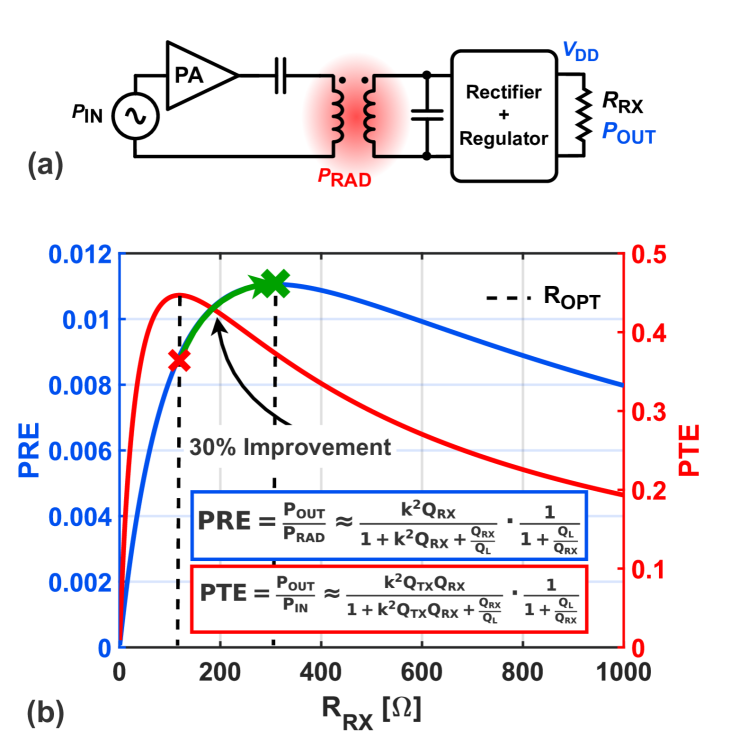
At the system level, the PMU is typically optimized for power transfer efficiency (PTE) at the expected system load [10, 11, 9]. In this approach, the optimal PTE is achieved only for a single load scenario, and any deviation in the system load corresponds to a deviation from the optimum. Furthermore, since the radiated power is proportional to the received voltage, the linear regulator in the PMU sets a lower limit on the power that needs to be radiated through the tissue to maintain a sufficiently high voltage for the load. Finally, the optimal PTE load focuses on the input power to the transmitter, and it does not necessarily minimize the radiated power into the tissue, which is the limiting factor for safety.
This letter presents two key concepts. (i) We introduce an active receiver (RX) rectifier with rapid ON/OFF adaptive delay compensation for a 40.68 MHz inductive WPT. The rectifier design implements a novel direct voltage-domain compensation and eliminates the need for a slow feedback control loop while maintaining high PCE under fast input or load variations. The high resonance frequency enables on-chip integration of the RX resonance and filter capacitor, requiring only a coil as an external component. A prototype of the fast-settling rectifier achieved a measured VCR of 93.9% and a simulated PCE of 90.1% in a 0.19 mm2 active area, which includes the resonant and filter capacitors. (ii) We propose a new link optimization method based on power radiated efficiency (PRE) that minimizes radiated power for a given output load. If combined with a switched capacitor power converter (SCPC), this approach simultaneously maintains optimum PRE across load variations and enables TX-side load monitoring to regulate the transmitted power.
II Power Radiated Efficiency
PRE is defined as the ratio between the power radiated by the TX antenna (PRAD) and the output power in the RX (POUT), while PTE is defined as the ratio between the input power to the TX power amplifier (PIN) and the output power in the RX (POUT). Since the TX is typically outside the body, its power efficiency is less critical and the main goal is to reduce the power radiated into the tissue. Hence, the objective is to maximize PRE and not PTE. A potential reduction of 30% in radiated power can be achieved in our WPT link (details in Section IV) by optimizing the RX tank load (RRX) for PRE rather than PTE, assuming no additional losses (Fig. 1(b)). This improvement occurs because the TX power sent to the resonant tank (PIN) is much smaller than the power in the tank itself, since most of the power is reactive.
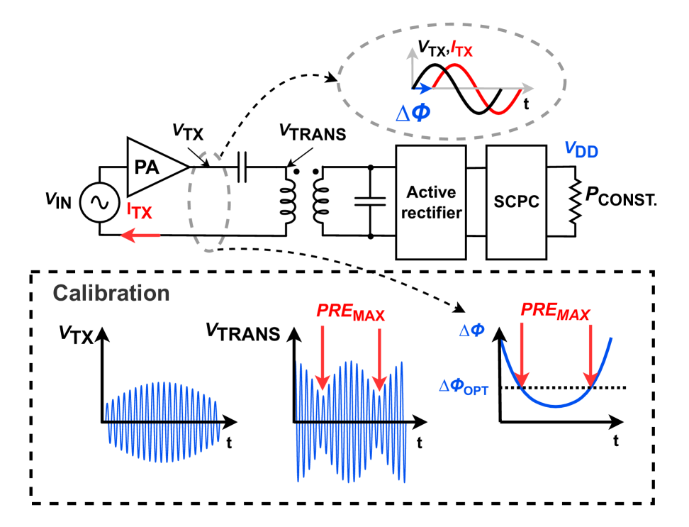
PRE optimization can be combined with a DC-DC converter after the rectification stage to transform any output load (RL) to an optimal RRX by allowing VTX to be decoupled from VDD. In this scenario, global power control is necessary to regulate the TX power and maintain optimum PRE over output load variations. This work introduces a TX-side-only load sensing for closed-loop regulation requiring only a phase measurement and a single calibration step (Fig. 2), similar to [7]. At startup, the implant is programmed to draw constant power (nominal light load), while the TX AC voltage (VTX) is swept over a predetermined range. The peak PRE is achieved when the VTRANS amplitude is minimal, since VTRANS is approximately proportional to the radiated power. Notably, the phase difference between VTX and ITX is proportional to RRX and can be used to track PRE. At startup, the phase difference for maximum PRE is measured (\textDelta\textPhiOPT). During normal operation, the TX power is regulated to maintain \textDelta\textPhiOPT.
III Active Rectifier with Delay Compensation
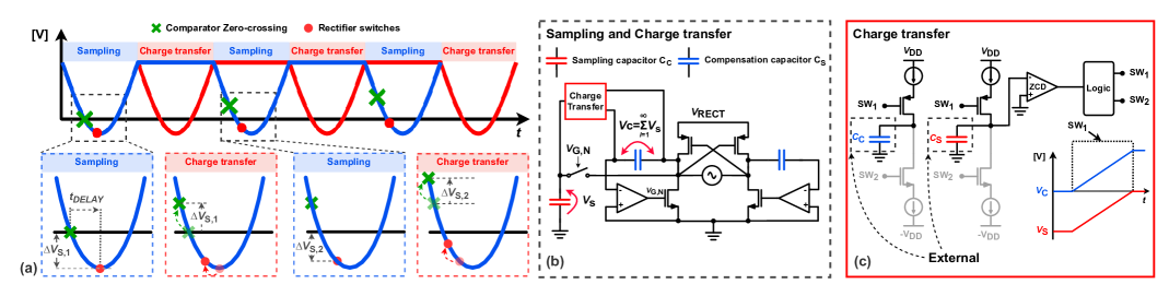
The delay compensation technique for the active rectifier in this work does not require a slow feedback control loop, as in previous works, to maintain system stability. Instead, it samples the error voltage () at the switching instant and adds it in series to the input of the comparator to compensate for the delay directly (Fig. 3(a)). A few accumulation cycles are typically sufficient to account for the nonlinear relationship between the error voltage and the required comparator offset to fully compensate the delay (simulated worst-case settling <200 ns). After system startup, this technique can continuously compensate for the delay in a single cycle (25 ns) over typical load and input variations (120 \textOmega - 1k\textOmega).
The delay compensation implementation is shown in Fig. 3(b-c), where each edge of the gate driving signals (VGN,1,VGN,2) has an independent compensation implementation. A sampling capacitor (CS) captures the error voltage at the switching instance of the rectifier, which is then transferred to a compensation capacitor (CC). A charge transfer circuit implements the sample-and-accumulate operation needed for the direct compensation technique using identical sampling and compensation capacitors. First, the polarity of the error voltage is determined to enable either the positive or negative charge-transfer current sources. Both capacitors are charged towards VDD (-VDD) in case of a negative (positive) voltage using nominally identical current sources. A zero-cross detector (ZCD) ends the charging period for both capacitors when the voltage in the sampling capacitor crosses 0 V. The result is that the charge in the sampling capacitor is added to the compensating capacitor. The capacitors have the same capacitance and then the corresponding voltages are VS and VC respectively as shown in Fig. 4. An additional safety circuit resets the compensation capacitor if it has an initial charge that disrupts the normal operation of the rectifier (VG,N is always 0). The ZCD and the comparator for the active diode in the rectifier are implemented using auto-zeroed inverters [12]. Level shifters are used to switch the MOSFETs between the capacitors and the -VDD rail and a SCPC generates -VDD on-chip.
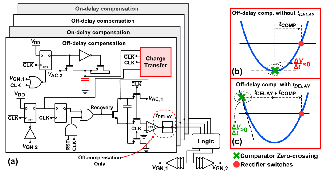
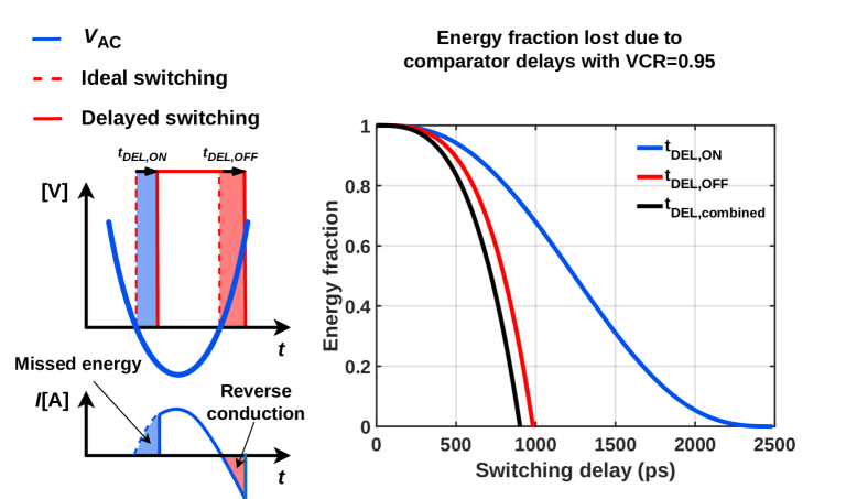
Setting identical compensation architectures for both ON- and OFF-delays would move the OFF-trigger point close to the trough of the AC input, where approaches zero, making the system sensitive to voltage errors (Fig. 4(b)). To address this issue, the OFF-compensation scheme adds a delay line, effectively shifting the OFF-trigger point to the same region as the ON-trigger point (Fig. 4(c)). The compensation settles with a small residual delay <200 ps, which is equivalent to <1% energy losses due to ON/OFF delay (Fig. 5).
IV Measurement Results
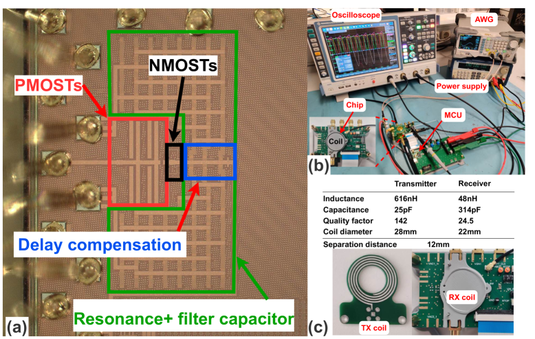
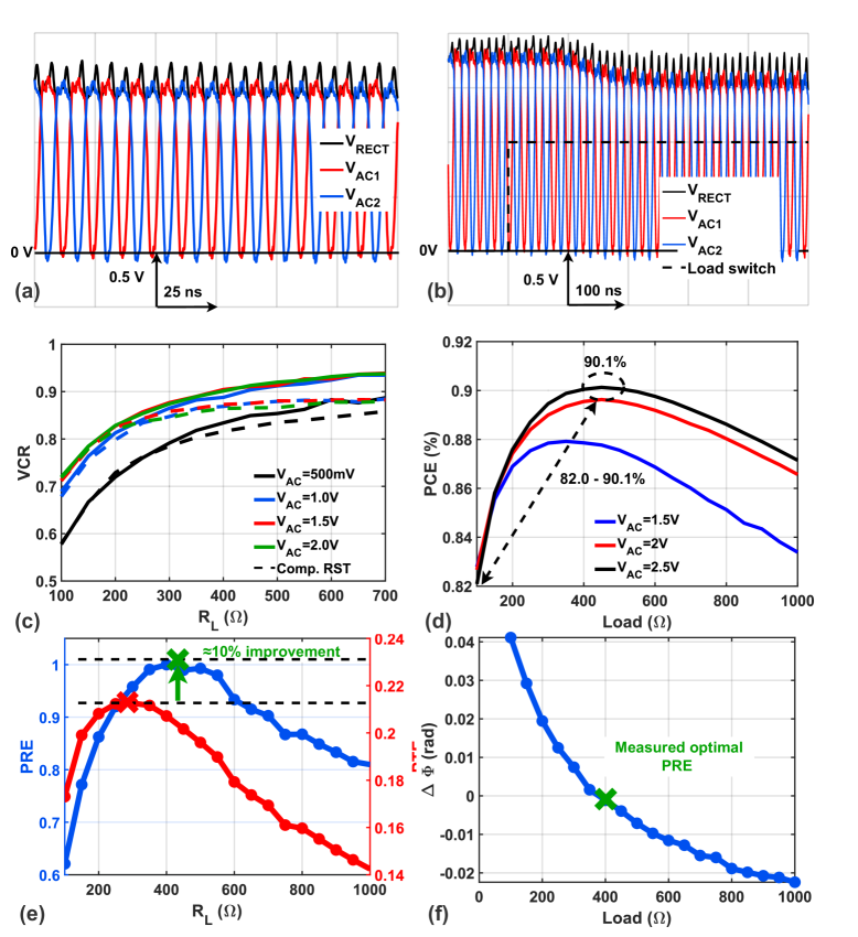
The proposed design was fabricated in a 40 nm CMOS process, occupying a chip area of 0.19 mm2. The measurement setup consists of a 616 nH PCB inductor and tunable capacitors driven by a power amplifier IC on the TX side, while an RX board containing the wire-bonded ASIC completes the link (Fig. 6). High-speed buffer ICs (LMH6559) were used to minimize parasitic loading and reduce interference from the inductive fields when measuring the AC signals in the link. The steady-state and settling behavior of the measured system are shown in Fig. 7(a-b).
Rapid settling of the output can be observed with a load change from 600 \textOmega to 300 \textOmega. The output pole formed by the capacitance of the on-chip filter and the load (RC = 150 ns) limits the settling of the rectifier and is consistent with the measurement results. It can be concluded that the compensation loop is likely faster, or as fast, as the observed settling. The delay compensation circuitry consumes only 130 µW. The measured voltage conversion ratio (VCR) shows a peak value of 93.9% with a 700 load (Fig. 7(c)). The PCE could not be measured due to complexities introduced by the on-chip capacitor and the UART communication interface, which made single-ended probing and direct driving of the chip impossible. The simulated PCE is shown in Fig. 7(f), with a peak efficiency of 90.1%.
The measurement results show a 10% improvement when optimizing for PRE, instead of PTE (Fig. 7(d)). The difference with the approximation in Fig. 1(b) is due to the fact that the measurement results include all losses experienced by the link. Any additional unmodeled losses are included in the radiated power, shifting the PTE curve closer to the PRE curve as link losses increase. Finally, the measured phase difference between VTX and ITX shows the dependence on RRX that can be used to regulate the TX power without the need for back communication from the implanted RX (Fig. 7(e)).
V Conclusion
This work achieves VCR and PCE comparable to the state-of-the-art, with a high power density across a wide AC input range and occupies only 0.19 mm2 (Table I). This performance is achieved while integrating the resonant capacitor on-chip and achieving the fastest delay compensation settling in literature. Additionally, we introduced a new link optimization approach that can reduce radiated power across any output load, thanks to a TX-side load sensing technique when a DC-DC converter is implemented in the power management unit.
![[Uncaptioned image]](/html/2506.07710/assets/x8.png)
Acknowledgments
The authors thank Brian Nanhekan, Zu-Yao Chang, Marco Pelk and Juan Bueno Lopez for technical support.
References
- [1] H.-M. Lee and M. Ghovanloo, “An Integrated Power-Efficient Active Rectifier With Offset-Controlled High Speed Comparators for Inductively Powered Applications,” IEEE Trans. Circuits Syst. I, vol. 58, no. 8, pp. 1749–1760, Aug. 2011.
- [2] L. Cheng, W.-H. Ki, Y. Lu, and T.-S. Yim, “Adaptive On/Off Delay-Compensated Active Rectifiers for Wireless Power Transfer Systems,” IEEE J. Solid-State Circuits, vol. 51, no. 3, pp. 712–723, Mar. 2016.
- [3] C. Huang, T. Kawajiri, and H. Ishikuro, “A Near-Optimum 13.56 MHz CMOS Active Rectifier With Circuit-Delay Real-Time Calibrations for High-Current Biomedical Implants,” IEEE J. Solid-State Circuits, vol. 51, no. 8, pp. 1797–1809, Aug. 2016.
- [4] Z. Xue, S. Fan, D. Li, L. Zhang, W. Gou, and L. Geng, “A 13.56 MHz, 94.1% Peak Efficiency CMOS Active Rectifier With Adaptive Delay Time Control for Wireless Power Transmission Systems,” IEEE J. Solid-State Circuits, vol. 54, no. 6, pp. 1744–1754, Jun. 2019.
- [5] Y. Lu and W.-H. Ki, “A 13.56 MHz CMOS Active Rectifier With Switched-Offset and Compensated Biasing for Biomedical Wireless Power Transfer Systems,” IEEE Trans. Biomed. Circuits Syst, vol. 8, no. 3, pp. 334–344, Jun. 2014.
- [6] J. Ahn, H.-S. Lee, K. Eom, W. Jung, and H.-M. Lee, “A 13.56-MHz 93.5%-Efficiency Optimal On/Off Timing Tracking Active Rectifier with Digital Feedback-Based Adaptive Delay Control,” IEEE Trans. Biomed. Circuits Syst, pp. 1–15, 2024.
- [7] X. Bai, Y. Lu, C. Zhan, and R. P. Martins, “A 6.78-MHz Wireless Power Transfer System With Inherent Wireless Phase Shift Control Without Feedback Data Sensing Coil,” IEEE J. Solid-State Circuits, vol. 58, no. 6, pp. 1746–1757, Jun. 2023.
- [8] Z. Luo, J. Liu, and H. Lee, “A 40.68-MHz Active Rectifier With Cycle-Based On-/Off-Delay Compensation for High-Current Biomedical Implants,” IEEE J. Solid-State Circuits, vol. 58, no. 2, pp. 345–356, Feb. 2023.
- [9] X. Li, C.-Y. Tsui, and W.-H. Ki, “A 13.56 MHz Wireless Power Transfer System With Reconfigurable Resonant Regulating Rectifier and Wireless Power Control for Implantable Medical Devices,” IEEE J. Solid-State Circuits, vol. 50, no. 4, pp. 978–989, Apr. 2015.
- [10] M. Kiani, “Wireless Power Transfer and Management for Medical Applications: Wireless power,” IEEE J. Solid-State Circuits, vol. 14, no. 3, pp. 41–52, 2022.
- [11] A. K. RamRakhyani, S. Mirabbasi, and M. Chiao, “Design and Optimization of Resonance-Based Efficient Wireless Power Delivery Systems for Biomedical Implants,” IEEE Trans. Biomed. Circuits Syst, vol. 5, no. 1, pp. 48–63, Feb. 2011.
- [12] W. J. Tenten and P. R. Shepherd, “New CMOS high-speed, high-accuracy auto-zero comparator design based on symmetric cross-coupled concepts,” IEEE J. Solid-State Circuits, vol. 68, no. 3, pp. 405–412, Mar. 1990.
- [13] S. Pal and W.-H. Ki, “40.68 MHz Digital On-Off Delay-Compensated Active Rectifier for WPT of Biomedical Applications,” IEEE Trans. Circuits Syst. II: Express Br., vol. 67, no. 12, pp. 3307–3311, Dec. 2020.
- [14] Z. Luo, J. Liu, and H. Lee, “A High-Efficiency 40.68-MHz Single-Stage Dual-Output Regulating Rectifier With ZVS and Synchronous PFM Control for Wireless Powering,” IEEE J. Solid-State Circuits, vol. 59, no. 8, pp. 2418–2429, Aug. 2024.