Defects and acceptor removal in 60Co -irradiated p-type silicon
Abstract
Boron-doped silicon detectors used in high radiation environments like the future HL-LHC show a degradation in device performance due to the radiation induced deactivation of the active boron dopant. This effect, known as the so-called Acceptor Removal Effect (ARE), depends on particle type, particle energy and radiation dose and is usually explained by the formation of boron-interstitial - oxygen-interstitial (BO) defects that induce a donor-type defect level in the upper part of the Si band gap. Here we present defect characterization studies using Thermally Stimulated Current technique (TSC) and Deep Level Transient Spectroscopy (DLTS) on a set of epitaxially grown p-type silicon diodes of different resistivity, irradiated with 60Co -rays. We used the defect parameters (activation energy, charge carrier capture cross sections and defect concentration) obtained from DLTS experiments for modeling the corresponding TSC spectra, and subsequently compared those with the experimental TSC results. This approach shows that the di-vacancy which is well characterized by DLTS correlates with the so-far unspecified charge emission signal of the X-defect that partially overlaps with the BO peak in TSC spectra. Additionally, in order to evaluate the impact of BO defect formation on the macroscopic properties of the device, we compared the BO defect concentration with the change in the effective carrier concentration N obtained from C-V measurements. It shows that the variations in N are about twice the changes in the BO concentration, which is in perfect consistency with the assumption of boron deactivation by the formation of the BO donor in irradiated p-type Si.
keywords:
60Co -rays , p-type silicon , defect spectroscopy , acceptor removal , DLTS , TSC , point defects[1]organization=European Organization for Nuclear Research, CERN,addressline=Esplanade des Particules 1, city=Geneva, postcode=1211, country=Switzerland
[2]organization=National Institute of Materials Physics, NIMP,addressline=Str. Atomistilor 105 bis, city=Bucharest, postcode=RO-77125, country=Romania
[3]organization=Institute for Experimental Physics, University of Hamburg,addressline=Luruper Chaussee 149, city=Hamburg, postcode=22761, country=Germany
[4]organization=Instituto de Física de Cantabria (IFCA), CSIC - Universidad de Cantabria,addressline=Avenida de los Castros, s/n, city=Santander, postcode=39005, country=Spain
[5]organization=Institute of Physics, Albert-Ludwigs-Universitaet Freiburg,addressline=Hermann-Herder-Strasse 3, city=Freiburg im Breisgau, postcode=79104, country=Germany
1 Introduction
Boron-doped silicon detectors (e.g. diodes, Low Gain Avalanche Detectors (LGADs) or HV-CMOS devices) used in high radiation environments like the future HL-LHC at CERN are impacted in their performance due to the radiation induced deactivation of the active boron dopant. This effect is known as the so-called Acceptor Removal Effect (ARE) and depends on particle type, particle energy and radiation dose [1, 2, 3, 4, 5, 6, 7, 8]. Briefly summarized, one assumes that the impinging high-energy particles induce a displacement damage in the silicon lattice creating Frenkel pairs composed of a silicon atom on an interstitial site (I) as well as a vacancy (V). Vacancies usually show low mobility at low temperature and mainly form vacancy-oxygen complexes or multi-vacancy defects (V, V, …). Si-interstitials however are very mobile even at cryogenic temperatures and interact via the Watkins replacement mechanism with impurities and dopants [9]. In boron-doped Si the two main interaction pathways result in the formation of boron-interstitials (B) and carbon-interstitials (C) which further interact with oxygen to boron-interstitial - oxygen-interstitial (BO) or carbon-interstitial - oxygen-interstitial (CO) defects [10, 11, 8]. The CO defect is known to be neutral in the space charge region, while the BO forms a donor-type defect level in the upper part of the Si band gap that introduces positive space charge [10]. Consequently, the formation of the BO defect deactivates in total two active boron dopants - one due to the inclusion of the BO defect and one by counterbalancing the negative space charge of a second boron by the positive space charge of the BO. Therefore, BO formation should correlate with a factor of two with the change in the effective space charge concentration N. Here it should be mentioned that in recent publications also immobile boron-substitutionals that are capturing Si-interstitials forming a so-called BSi defects are considered to explain the ARE [12]. However, in this publication we will follow the so far widely accepted assumption of a BO defect structure.
Besides the discussed point-like defects, high energetic radiation induced displacements also create cluster-like defects that significantly impact the performance of silicon detectors [7, 13, 14]. However, by performing radiation studies using low-energy electrons or -radiation the creation of large cluster complexes is very unlikely, and thus, it becomes possible to directly correlate changes in the macroscopic device properties, like the change in N, with changes in concentrations of point-like defects like the BO [9, 13, 15].
In this work, we present defect spectroscopy studies in combination with electrical characterization as well as theoretical modeling approaches on -irradiated p-type silicon diodes of different resistivity with the intention to further deepen and intensify the knowledge of radiation induced point-like defects and their impact on the performance of Si based devices.
| resitivity | nominal dose | IR | ||
|---|---|---|---|---|
| [cm] | [MGy] | [106 cm-3/Gy] | ||
| BO | CO | |||
| EPI-06-DS-67 | 50 | 0.1 | 6.3 | 1.1 |
| EPI-06-DS-69 | 50 | 0.2 | 6.7 | 1.4 |
| EPI-06-DS-82 | 50 | 1 | 5.8 | 1.5 |
| EPI-06-DS-84 | 50 | 2 | 5.5 | 1.4 |
| EPI-10-DS-78 | 250 | 0.1 | 4.4 | 4.4 |
| EPI-10-DS-80 | 250 | 0.2 | 4.5 | 4.7 |
| EPI-10-DS-82 | 250 | 1 | 4.8 | 5.2 |
| EPI-10-DS-94 | 250 | 2 | 4.7 | 5.1 |
2 Materials and methods
The experimental studies were performed on a set of boron-doped silicon pad diodes with structure manufactured by CiS (Forschungsinstitut für Mikrosensorik GmbH, Erfurt, Germany) [16]. They consist of an 50 \unit\micro boron-doped bulk layer of either 50 cm or 250 cm resistivity epitaxially grown on a low resistivity substrate. The active area of the devices is cm2. More details about the diodes can be found in Ref. [17] and [18]. The devices were irradiated at the 60Co source of the Ruder Boskovic Institute (RBI) in Zagreb, Croatia with doses in the range of 0.1 to 2 MGy [15]. An overview of the sensors and radiation doses is given in Tab.1. After irradiation, performed at room temperature, the sensors were not intentionally annealed. They were kept at temperatures below - 20∘C also during the transport.
In order to investigate radiation induced macroscopic changes of the device properties, Capacitance-Voltage (C-V, measurement frequency 10 kHz, parallel mode) and Current-Voltage (I-V) measurements were performed at - 20∘C. During all measurements the guard ring of the diodes was connected to ground.
C-V measurements were used to extract the effective carrier concentrations N of the irradiated diodes using the following equations [19]:
| (1) |
| (2) |
with: - the dielectric constant, q - the elementary charge, A - the electrode area of the diode, w - the thickness of the depleted region and d(1/C)/dV - the slope of the 1/C versus voltage curve.
To characterize the radiation induced defects in the investigated diodes, Deep-Level-Transient Spectroscopy (DLTS) and Thermally Stimulated Current technique (TSC) were used. Both methods can be used to extract defect parameters like thermal activation energy E of defect levels, capture cross sections for electrons and holes and defect concentration N. While DLTS technique is based on analyzing the measured capacitance transients following injection pulses for filling the traps at each temperature step, in TSC the quasi-equilibrium currents generated by emission of charge from the traps filled at low temperature (single shot injection) are used to determine the properties and concentration of defects. In TSC, the occupation of the defect levels was done by cooling down the diodes under reverse bias (UR) to a filling temperature T where the filling of the traps was performed either with majority carriers (holes) by setting the bias voltage to around 0 V for a certain filling time t, or with both, minority and majority carriers (electrons and holes) by applying a forward bias of + 20 V, corresponding to a filling current of about 1 mA which was set as compliance for the source meter. A more detailed description of both techniques can be found in Ref. [20, 21, 18, 22, 23].
In order to compare defect levels identified by DLTS with those measured with TSC we used the defect parameters obtained by DLTS to model TSC spectra by using a Python-based analysis software pytsc. Within pytsc the diode is treated as one-dimensional device with a homogeneous dopant and defect distribution inside the sensor volume. The discharging TSC current is given by the following equation [24]:
| (3) |
where e(t) and e(t) are the emission rates for electrons and holes while n(t) and p(t) are the fraction of defect states occupied by electrons or holes. For the simulation the sensor bulk volume is sliced into N differential parts of thickness z and n is the number of fully depleted slices. This number depends on the applied bias voltage as well as the effective carrier concentration N, both defining the depletion depth (equivalent to equation 2). N can set constant or dynamic (N = N + N(t)) within pytsc. For the results presented in this paper N was always set constant.
The emission rate for electrons or holes from a single trap is given by:
| (4) |
with (E,T) giving the enhanced emission probability, in dependence of the position dependent electric field distribution E and the temperature T, due to the Poole-Frenkel effect, and
, including a constant B, the effective mass m as well as thermal velocity of the carriers. is the cross section and E is the activation energy. In the modeling given in this publication the influence of the Poole-Frenkel effect is not included, so (E,T) was set to one.
The number of defect states occupied by electrons n(t) (and equivalent for holes p(t)) at a certain time t is given by:
| (5) |
For the modeling with pytsc presented in this publication, as absolute trap concentrations N, capture cross sections and activation energies, experimentally determined values from corresponding DLTS measurements were used.
3 Results and Discussion
3.1 Electrical Characterization
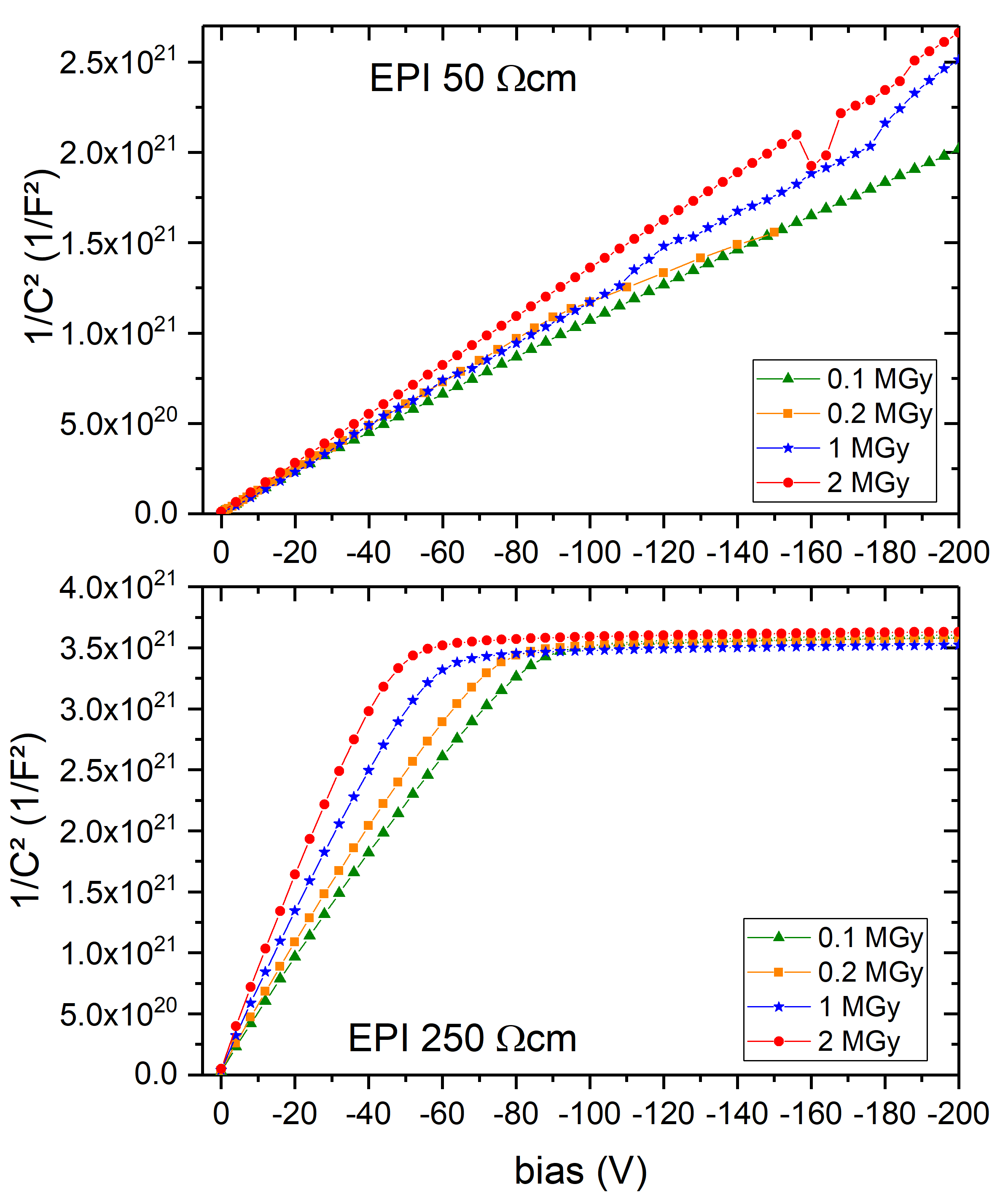
All samples were electrically characterized before and after irradiation. In Fig.1 capacitance-voltage (C-V) measurements performed on 50 cm (top) and 250 cm (bottom) EPI diodes are plotted. The curves were recorded after 60Co gamma irradiation with different doses. Due to the high doping, the 50 cm sensors could not be fully depleted in the applied voltage range. The full depletion voltage V of the 250 cm sensors, extracted from the kink in the curves, decreases from about - 82 V after 0.1 MGy irradiation to about - 45 V after 2 MGy irradiation.
From the C-V measurements the effective carrier concentrations N were extracted using equation 1 and 2.
The values are plotted in Fig. 6 and will be discussed in section 3.2.
Current-voltage (I-V) measurements on the 60Co gamma irradiated EPI diodes (not illustrated here) have shown an increase of the leakage current with increasing radiation dose.
3.2 DLTS studies
In Fig. 2 and 3 the measured DLTS spectra of the -irradiated 50 cm and 250 cm sensors are presented. The upper spectra in Fig. 2 and Fig. 3 were obtained by applying a pulse voltage UP of -0.6 V corresponding to majority carrier injection (only hole traps are detected), while the lower spectra were obtained after applying UP = + 2 V leading to majority and minority carrier injection (hole and electron traps can be detected).
For both sensor types four pronounced defect levels are detected, three hole traps and one electron trap, labeled as (1), (2), CO (carbon-intersital - oxygen-interstitial) and BO (boron-interstitial - oxygen-interstitial), respectively. By analysing the Arrhenius-plots resulted from the DLTS spectra corresponding to different time windows (TW) the following defect parameters were obtained for the detected levels:
peak (1): E + 0.09 eV and : 210-14 cm2
peak (2): E + 0.19 eV and : 410-16 cm2
CO: E + 0.36 eV and :210-15 cm2
BO: E - 0.25 eV and : 610-15 cm2
In Addition, for peak (2) direct capture cross section measurements were performed, giving a value of = 710-16 cm2.
For the CO and BO defect the values are in good agreement with data from the literature. Also for peak (1) and peak (2) an assignment can be given by comparing the defect parameters to DLTS data in the literature [9, 11, 25, 26, 27, 28, 29, 30, 31]. Thereby, peak (1) may be related to an di-self-interstial - oxygen-interstitial (I2O) defect, while the characteristics of peak (2) are comparable to a vacancy related defect level: the single-positive charge state of the di-vacancy V(0/+) .
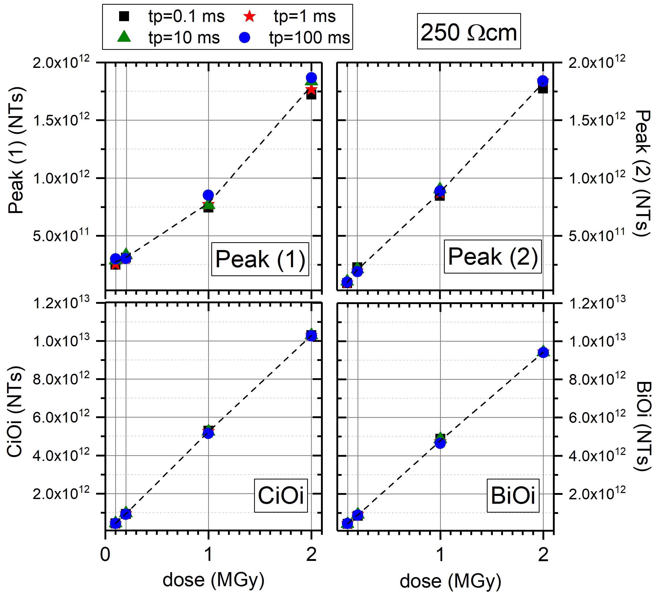
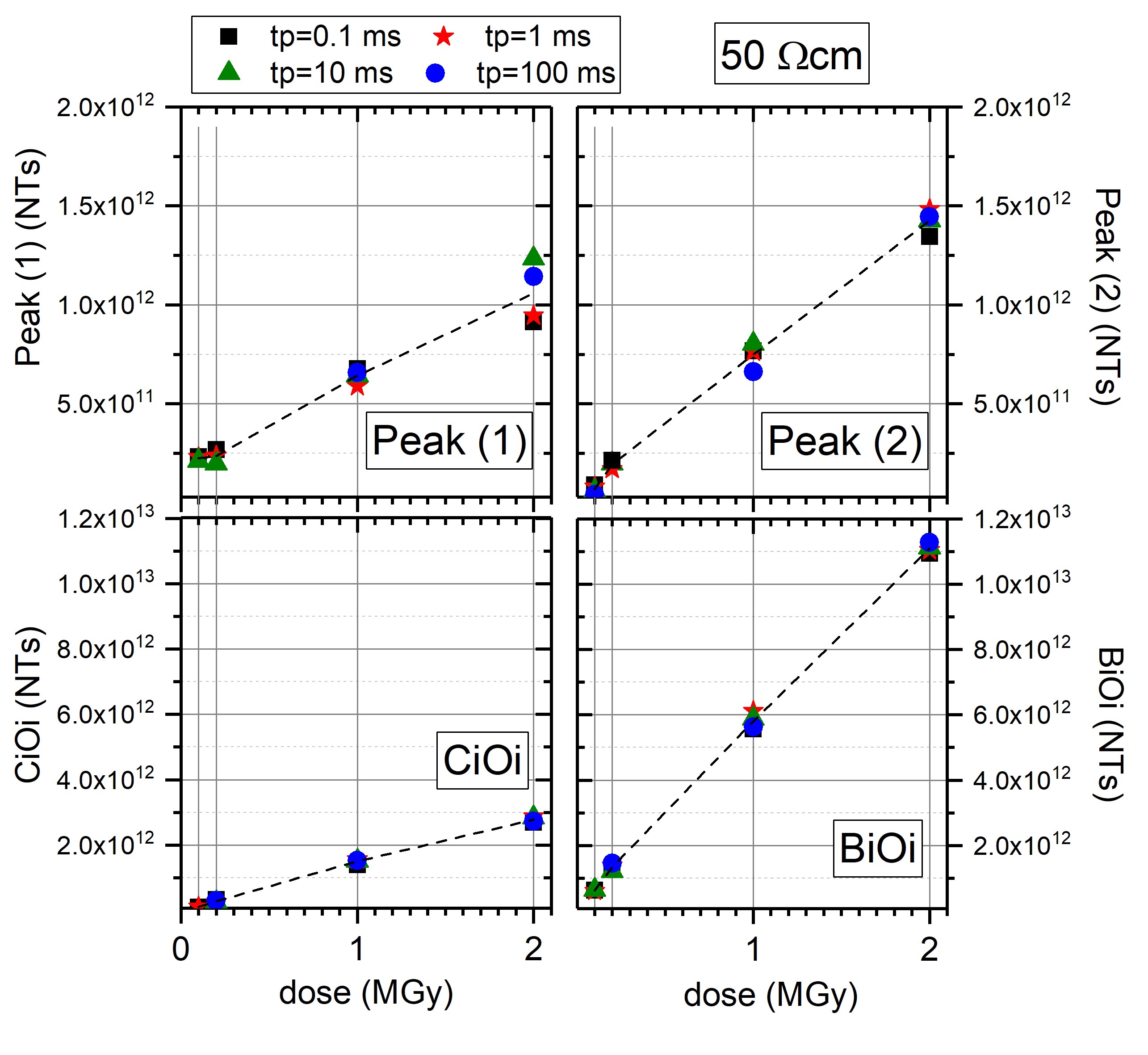
The extracted concentrations for the detected defects as function of radiation dose are given in Fig.4 and Fig. 5 for the 50 cm and the 250 cm sensors, respectively. The different symbols for one radiation dose correspond to measurements with different duration of the injection pulse (t) from 0.1 ms up to 100 ms.
No significant dependence of the extracted defect concentrations on the pulse time was found. The defect concentrations of peak (2), CO and BO increase linearly with radiation dose, while for the high resistivity diode, the increase of the defect concentration of peak (1) is steeper at a higher radiation dose. In table 1 the corresponding introduction rates for the BO and CO are listed.
Concerning differences in the absolute defect concentrations between the 50 cm and the 250 cm diodes, it can be observed, that for peak (1) and peak (2) the defect concentrations are slightly higher for the 250 cm diodes. In the 50 cm diodes the BO concentration dominates due to the high boron content in the samples.
The CO concentration is rather low in these diodes, especially compared to those of 250 cm where the CO to BO ratio is 1.
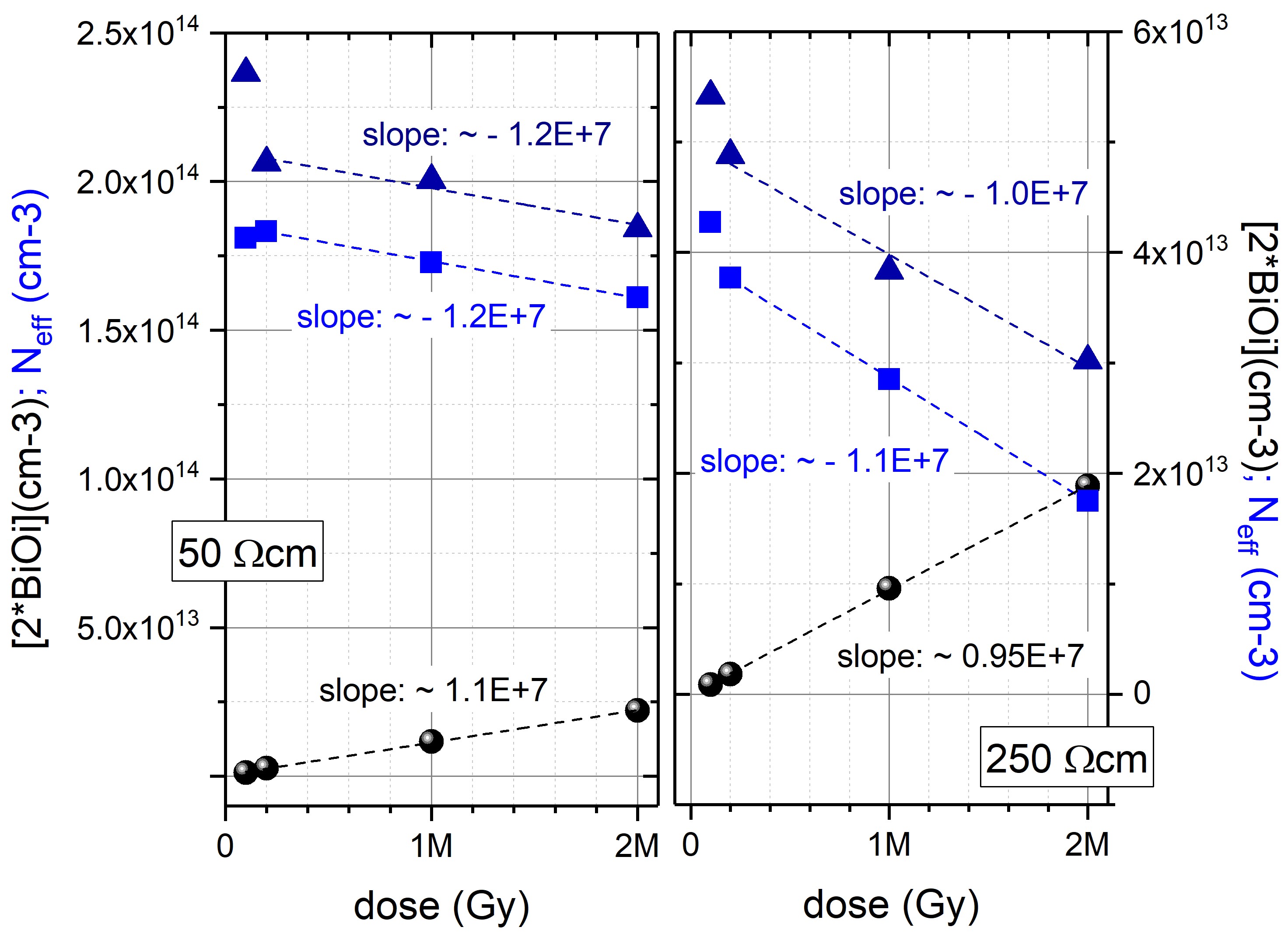
Fig.6 shows the correlation between the BO concentration (taken twice) and the change in the effective doping concentration N of the irradiated 50 cm and 250 cm diodes. For N two different values are plotted in Fig. 6. The values depicted by blue triangles were extracted from the C-V measurements shown in Fig. 1 that were performed at 253 K and 1 kHz. The N values depicted by blue squares were extracted from C-V measurements performed during the DLTS scan at 1 MHz in the temperature range of BO charge emission (T = 108 - 130 K). The slope of both curves is comparable and correlates very well with the change in BO concentration for doses 200 kGy. The observed correlation supports the assumption that the BO formation is the main responsible mechanism for acceptor removal in irradiated boron-doped silicon. Thereby, the formation of one BO would deactivate two active boron atoms. The presented results are in good agreements with similar measurements on proton irradiated epitaxial silicon diodes [22].
3.3 Analysis and modeling of TSC spectra
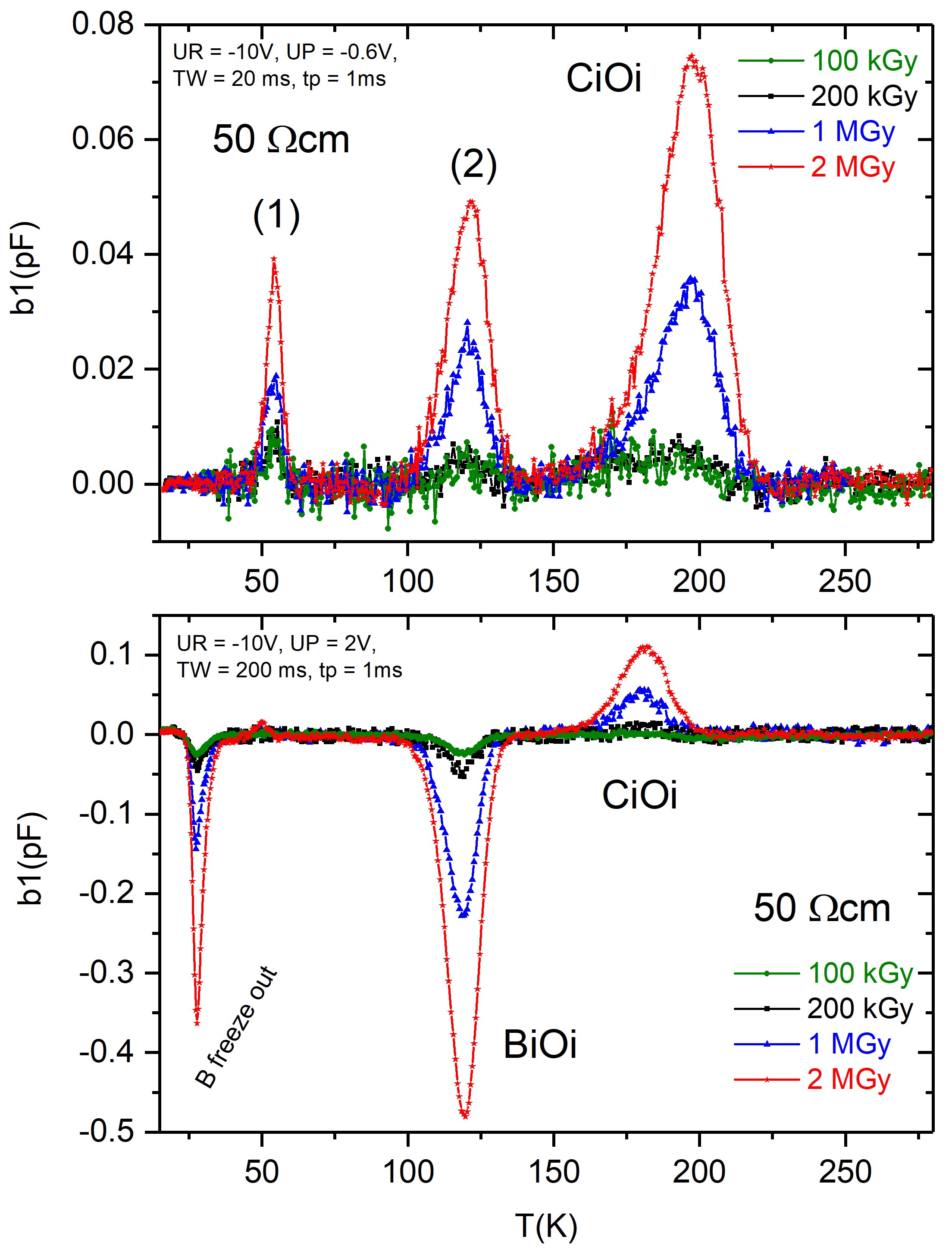
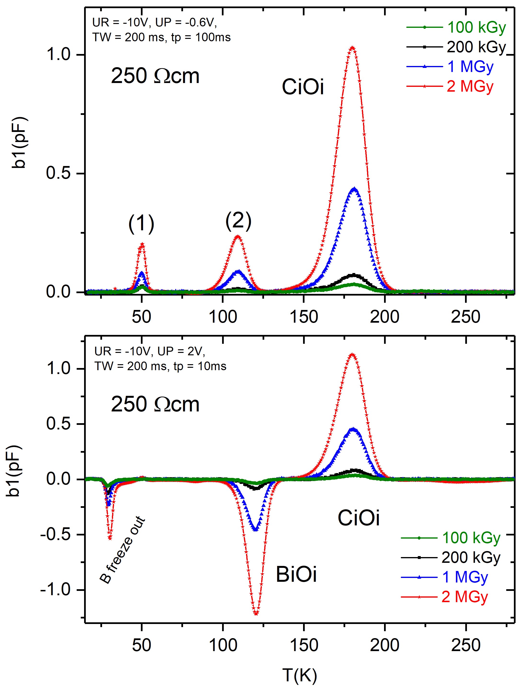
Besides DLTS investigations also TSC measurements in the temperature range of 20 K to 220 K were performed on the -irradiated EPI diodes. Fig. 7 shows as example the TSC spectra measured on the 250 cm EPI diode -irradiated with 2 MGy. Five prominent TSC peaks are revealed by these experiments, three belonging to hole traps labeled as H(40), X-defect and CO and two to electron traps, VO and BO. The filling pulse voltage UP of the first two spectra in Fig. 7 was set to a forward bias of + 20 V while the filling temperature T was varied. This was done since the electrical filling of defects like CO and X-defect is temperature dependent when injecting with forward bias [14, 22]. Their TSC signal intensity starts to increase with increasing T. In Fig. 7 (grey line-square spectrum) the X-defect as well as the CO are shown after carrier injection at 75 K. The X-defect is partly overlapping with the BO peak.

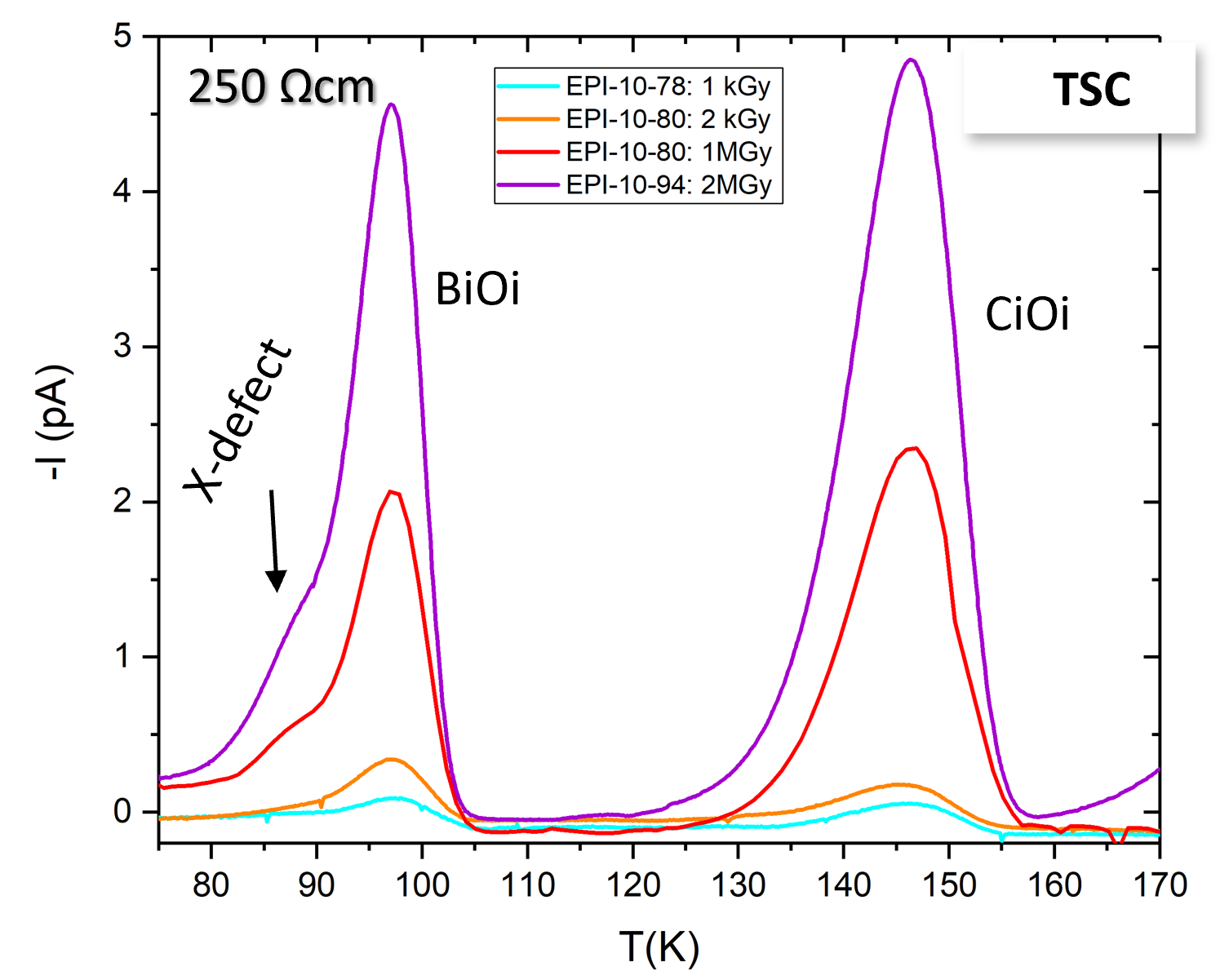
In order to separate these peaks and distinguish the defect levels between electron and hole traps, TSC spectra with filling pulse UP = 0 V were also recorded. In this case only majority carriers were injected and the detected peaks H(40), X-defect and CO can be assigned to hole traps. The BO and the VO which are known to be electron traps [11, 32] are not detected in this case (see red line-dotted spectra in Fig.7).
For the 50 cm EPI diodes comparable measurements were performed (not shown here, see Ref.[33]) and allowed also the clear identification of three peaks: the X-defect, the BO and the CO defect. Since in the lower temperature range the measured spectra of the 50 cm diodes were dominated by a high setup-induced noise signal no information about defects with peak positions 60 K can be given at this point.
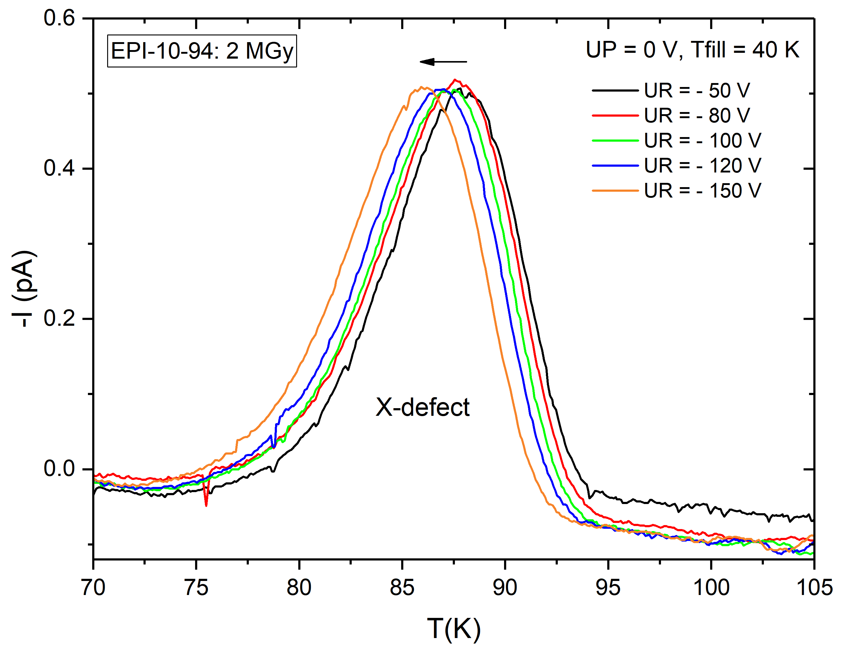
The clear assignment of the X-defect to a defect structure is still missing, although some specifications are already given in the literature [22, 23]. Shortly summarized, it is known, that the X-defect is a hole trap with a strongly temperature dependent capture cross section, as also presented in the measurements discussed before. Furthermore, detailed studies within the RD50 collaboration on proton, neutron and electron irradiated p-type silicon diodes stated that the X-defect can always clearly be identified by TSC for lower irradiation fluences ( \unitn_eq\per\centi□), while for higher fluences it is usually not seen. Additionally, the peak position of the X-defect in the TSC spectra shows a strong field dependence that was usually explained by the Poole-Frenkel effect [22, 23, 34]. This was also observed for the irradiated diodes presented in this paper. Corresponding TSC measurements are plotted in Fig.8. Here the charge emission from the X-defect was measured after cooling down the sample under reverse bias of -100 V, choosing a filling pulse of UP = 0 V and setting different reverse bias voltages UR when ramping up the temperature. With increasing the applied reverse bias UR in the range from - 50 V to - 150 V the X-defect peak position shifts to lower temperatures, indicating an electrical field dependence.
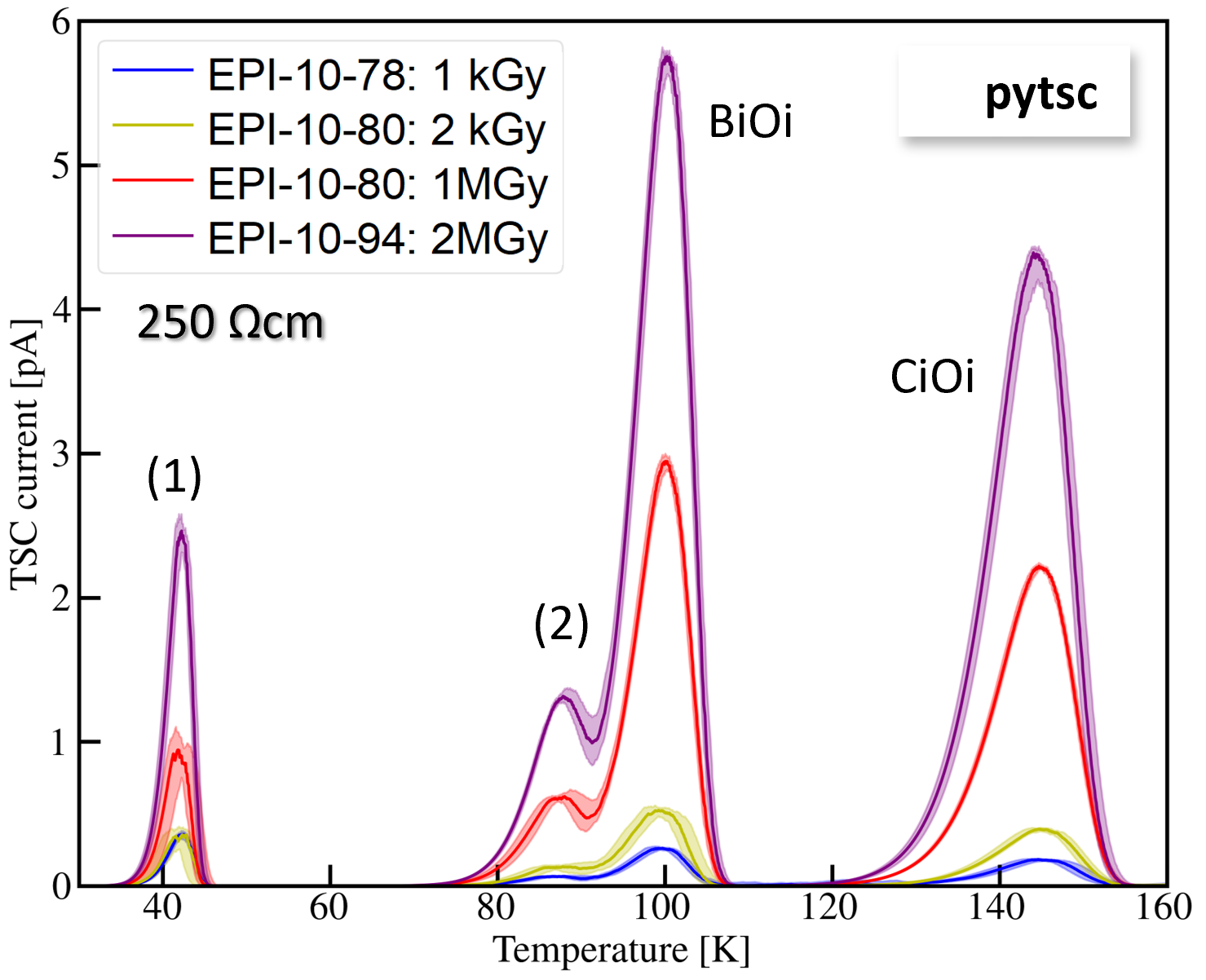
In order to promote the assignment of the defect levels detected in TSC, especially the X-defect, the measured TSC spectra were compared to modeled pytsc-spectra as described in section 2. As defect parameters for the pytsc modeling, data were taken that resulted from the DLTS experiments performed on the same sample. In Fig. 10 pytsc spectra of the -irradiated 250 cm EPI diode are presented. They can be compared to the measured TSC spectra illustrated in Fig. 9. The spectra of the 50 cm EPI diodes (see Ref. [33]) are comparable in the interpretation of the results to the 250 cm ones and therefore not additionally illustrated in this publication. The 4 peaks in Fig. 10 correspond to peak (1), peak (2), as well as BO and CO identified in DLTS (see Fig. 2 and 3). The peak amplitudes increase with increasing radiation dose. The same is observed in the TSC measurements (see Fig. 9), although there is a difference in the absolute peak heights. The modeled BO and CO peak positions are in very good agreement to the measured ones. The DLTS-Peak (2) gives in pytsc a signature next to the BO that strongly resembles the shoulder induced by the X-defect in TSC, while the position of DLTS-peak (1) correlates with the H(40) defect (see Fig. 7 and Fig. 10). As mentioned in section 3.2 the DLTS defect characteristics of peak (1) are comparable to those of the I2O defect, that points towards a correlation between the TSC H(40) peak and the I2O defect. For peak (2) the comparison of our DLTS results with literature, as discussed before in section 3.2, points to the donor state of the divacancy V2(0/+). This defect is neutral before trapping a hole and positively charged afterwards.Therefore, according to the definition of the Poole-Frenkel effect that occurs only for coulombic centers, the emission rate of the defect should not vary with the applied electric field. However, a large field dependence is reported in literature for the V2(0/+) and correlated with phonon assisted tunneling [26, 27]. Also the X-defect showed a field dependence when varying the reverse bias applied during TSC measurements. These are indications to assign the X-defect to a di-vacancy structure while still further work is needed to fully consolidate or decline this attribution.
4 Summary and Conclusion
The present work is summarizing defect studies on a set of epitaxial grown 60Co -irradiated p-type silicon diodes of different resistivity. In this context, it is demonstrated that the observed changes in the effective carrier concentration of the diodes correlate, as expected, with the formation of the boron-related BO defect. We clearly demonstrate that change of the effective space charge is double of the change of the BO defect concentration. This is fully consistent with describing the acceptor removal in boron doped p-type silicon as a process consisting of the removal of the shallow acceptor boron B and the subsequent formation of a BO defect with donor character, i.e. a positive space charge contributor. Additionally, within this work, a continuative defect analysis method is presented by combining results from different spectroscopic methods (DLTS and TSC) by implementing a Python-based modeling software (pytsc). Thereby, the defect parameters (activation energy, charge carrier capture cross section and defect concentration) obtained by DLTS are used for modeling the corresponding TSC spectra and comparing them with the experimental ones. It gives indications that the so-far unspecified X-defect, giving rise to a TSC peak that partially overlaps with that of BO, might be related to divacancies. However, further studies are needed and planned to fully confirm this assignment option.
5 Acknowledgement
The work was partly performed in the framework of the CERN RD50 and DRD3 collaborations. I. Pintilie acknowledge the funding received through IFA-CERN-RO 08/2022 project.
References
- [1] R. Wunstorf, W. Bugg, J. Walter, F. Garber, D. Larson, Investigations of donor and acceptor removal and long term annealing in silicon with different boron/phosphorus ratios, Nucl. Instrum. Methods Phys. Res. A 377 (2) (1996) 228–233, proceedings of the Seventh European Symposium on Semiconductor. doi:https://doi.org/10.1016/0168-9002(96)00217-3.
- [2] S. Terada, H. Iwasaki, T. Kohriki, T. Kondo, M. Numajiri, Y. Unno, T. Handa, Y. Iwata, T. Ohsugi, N. Tamura, R. Takashima, Proton irradiation on p-bulk silicon strip detectors using 12 GeV PS at KEK, Nucl. Instrum. Methods Phys. Res. A 383 (1) (1996) 159–165. doi:https://doi.org/10.1016/S0168-9002(96)00748-6.
- [3] G. Kramberger, M. Baselga, V. Cindro, P. Fernandez-Martinez, D. Flores, Z. Galloway, A. Gorišek, V. Greco, S. Hidalgo, V. Fadeyev, I. Mandić, M. Mikuž, D. Quirion, G. Pellegrini, H.-W. Sadrozinski, A. Studen, M. Zavrtanik, Radiation effects in Low Gain Avalanche Detectors after hadron irradiations, Journal of Instrumentation 10 (07) (2015) P07006. doi:10.1088/1748-0221/10/07/P07006.
-
[4]
H. F.-W. Sadrozinski, A. Seiden, N. Cartiglia,
4D tracking with
ultra-fast silicon detectors, Reports on Progress in Physics 81 (2) (2017)
026101.
doi:10.1088/1361-6633/aa94d3.
URL https://dx.doi.org/10.1088/1361-6633/aa94d3 - [5] G. Kramberger, M. Carulla, E. Cavallaro, V. Cindro, D. Flores, Z. Galloway, S. Grinstein, S. Hidalgo, V. Fadeyev, J. Lange, I. Mandić, G. Medin, A. Merlos, F. McKinney-Martinez, M. Mikuž, D. Quirion, G. Pellegrini, M. Petek, H.-W. Sadrozinski, A. Seiden, M. Zavrtanik, Radiation hardness of thin Low Gain Avalanche Detectors, Nucl. Instrum. Methods Phys. Res. A 891 (2018) 68–77. doi:https://doi.org/10.1016/j.nima.2018.02.018.
- [6] M. Ferrero, R. Arcidiacono, M. Barozzi, M. Boscardin, N. Cartiglia, G. D. Betta, Z. Galloway, M. Mandurrino, S. Mazza, G. Paternoster, F. Ficorella, L. Pancheri, H.-F. W. Sadrozinski, F. Siviero, V. Sola, A. Staiano, A. Seiden, M. Tornago, Y. Zhao, Radiation resistant LGAD design, Nucl. Instrum. Methods Phys. Res., Sect. A 919 (2019) 16–26. doi:10.1016/j.nima.2018.11.121.
- [7] M. Moll, Displacement Damage in Silicon Detectors for High Energy Physics, IEEE Transactions on Nuclear Science 65 (8) (2018) 1561–1582. doi:10.1109/TNS.2018.2819506.
- [8] M. Moll, Acceptor removal - Displacement damage effects involving the shallow acceptor doping of p-type silicon devices, PoS Vertex2019 (2020) 027. doi:10.22323/1.373.0027.
-
[9]
G. D. Watkins,
Intrinsic
defects in silicon, Materials Science in Semiconductor Processing 3 (4)
(2000) 227–235.
doi:https://doi.org/10.1016/S1369-8001(00)00037-8.
URL https://www.sciencedirect.com/science/article/pii/S1369800100000378 - [10] L. C. Kimerling, M. Asom, J. Benton, P. Drevinsky, C. Caefer, Interstitial Defect Reactions in Silicon, in: Defects in Semiconductors 15, Vol. 38 of Materials Science Forum, Trans Tech Publications Ltd, 1989, pp. 141–150. doi:10.4028/www.scientific.net/MSF.38-41.141.
- [11] P. M. Mooney, L. J. Cheng, M. Süli, J. D. Gerson, J. W. Corbett, Defect energy levels in boron-doped silicon irradiated with 1-MeV electrons, Phys. Rev. B 15 (1977) 3836–3843. doi:10.1103/PhysRevB.15.3836.
- [12] K. Lauer, K. Peh, S. Krischok, S. Reiß, E. Hiller, T. Ortlepp, Development of Low-Gain Avalanche Detectors in the frame of the acceptor removal phenomenon, Phys. Status Solidi (a) 219 (2200177) (2020). doi:10.1002/pssa.202200177.
- [13] I. Pintilie, G. Lindstroem, A. Junkes, E. Fretwurst, Radiation-induced point- and cluster-related defects with strong impact on damage properties of silicon detectors, Nucl. Instrum. Methods Phys. Res. A 611 (1) (2009) 52–68. doi:10.1016/j.nima.2009.09.065.
- [14] I. Pintilie, E. Fretwurst, G. Lindström, Cluster related hole traps with enhanced-field-emission - the source for long term annealing in hadron irradiated Si diodes, Appl. Phys. Lett. 92 (2) (2008) 024101. doi:10.1063/1.2832646.
- [15] C. Liao, E. Fretwurst, E. Garutti, J. Schwandt, I. Pintilie, A. Nitescu, A. Himmerlich, M. Moll, Y. Gurimskaya, Z. Li, Investigation of high resistivity p-type FZ silicon diodes after 60Co -irradiation, Nucl. Instrum. Methods Phys. Res. A 1061 (2024) 169103. doi:https://doi.org/10.1016/j.nima.2024.169103.
- [16] CiS Forschungsinstitut für Mikrosensorik GmbH, https://www.cismst.de/, (accessed on January 30th, 2024).
- [17] Y. Gurimskaya, P. Dias de Almeida, M. Fernandez Garcia, I. Mateu Suau, M. Moll, E. Fretwurst, L. Makarenko, I. Pintilie, Radiation damage in p-type EPI silicon pad diodes irradiated with protons and neutrons, Nucl. Instrum. Methods Phys. Res. A 958 (2020) 162221. doi:10.1016/j.nima.2019.05.062.
- [18] A. Himmerlich, N. Castello-Mor, E. C. Rivera, Y. Gurimskaya, V. Maulerova-Subert, M. Moll, I. Pintilie, E. Fretwurst, C. Liao, J. Schwandt, Defect characterization studies on irradiated boron-doped silicon pad diodes and Low Gain Avalanche Detectors, Nucl. Instrum. Methods Phys. Res. A 1048 (2023) 167977. doi:https://doi.org/10.1016/j.nima.2022.167977.
- [19] D. K. Schroder, Semiconductor Material and Device Characterization, 3rd Edition, John Wiley & Sons, Inc., New Jersey, 2006.
- [20] S. Weiss, R. Kassing, Deep Level Transient Fourier Spectroscopy (DLTFS)—A technique for the analysis of deep level properties, Solid-State Electronics 31 (12) (1988) 1733–1742. doi:https://doi.org/10.1016/0038-1101(88)90071-8.
- [21] I. Pintilie, L. Pintilie, M. Moll, E. Fretwurst, G. Lindstroem, Thermally stimulated current method applied on diodes with high concentration of deep trapping levels, Appl. Phys. Lett. 78 (4) (2001) 550–552. doi:10.1063/1.1335852.
- [22] C. Liao, E. Fretwurst, E. Garutti, J. Schwandt, M. Moll, A. Himmerlich, Y. Gurimskaya, I. Pintilie, A. Nitescu, Z. Li, L. Makarenko, The boron-oxygen (BiOi) defect complex induced by irradiation with 23 GeV protons in p-type epitaxial silicon diodes, IEEE Trans. Nucl. Sci. 69 (3) (2022) 576–586. doi:10.1109/TNS.2022.3148030.
- [23] C. Liao, E. Fretwurst, E. Garutti, J. Schwandt, L. Makarenko, I. Pintilie, L. D. Filip, A. Himmerlich, M. Moll, Y. Gurimskaya, Z. Li, Investigation of the Boron removal effect induced by 5.5 MeV electrons on highly doped EPI- and Cz-silicon, Nucl. Instrum. Methods Phys. Res. A 1056 (2023) 168559. doi:https://doi.org/10.1016/j.nima.2023.168559.
- [24] M. Moll, Radiation damage in silicon particle detectors, PhD thesis, Uni Hamburg, 1999. doi:10.3204/PUBDB-2016-02525.
- [25] E. G. Seebauer, M. C. Kratzer, Charged Semiconductor Defects: Structure, Thermodynamics and Diffusion, 1st Edition, Springer-Verlag London Limited, 2009.
- [26] N. Zangenberg, J.-J. Goubet, A. Nylandsted Larsen, On-line DLTS investigations of the mono- and di-vacancy in p-type silicon after low temperature electron irradiation, Nucl. Instrum. Methods Phys. Res. B 186 (1) (2002) 71–77. doi:10.1016/S0168-583X(01)00876-X.
- [27] N. R. Zangenberg, A. Nylandsted Larsen, On-line DLTS investigations of vacancy related defects in low-temperature electron irradiated, boron-doped Si, Appl. Phys. A 80 (2005) 1081–1086. doi:10.1007/s00339-003-2358-3.
- [28] D. A. Aharodnikau, S. B. Lastovskii, S. V. Shpakovski, V. P. Markevich, M. P. Halsall, A. R. Peaker, The Role of Si Self-interstitial Atoms in the Formation of Electrically Active Defects in Reverse-Biased Silicon n+–p Diodes upon Irradiation with Alpha Particles, Phys. Status Solidi (a) 218 (23) (2021) 2100104. doi:https://doi.org/10.1002/pssa.202100104.
- [29] V. P. Markevich, L. I. Murin, S. B. Lastovskii, I. F. Medvedeva, B. A. Komarov, J. L. Lindström, A. R. Peaker, Electrically active radiation-induced defects in Czochralski-grown Si with low carbon content, Journal of Physics: Condensed Matter 17 (22) (2005) S2331. doi:10.1088/0953-8984/17/22/022.
- [30] V. P. Markevich, A. R. Peaker, B. Hamilton, V. E. Gusakov, S. B. Lastovskii, L. I. Murin, N. Ganagona, E. Monakhov, B. G. Svensson, Structure, Electronic Properties and Annealing Behavior of Di-Interstitial-Oxygen Center in Silicon, in: Gettering and Defect Engineering in Semiconductor Technology XVI, Vol. 242 of Solid State Phenomena, Trans Tech Publications Ltd, 2016, pp. 290–295. doi:10.4028/www.scientific.net/SSP.242.290.
- [31] V. E. Gusakov, S. B. Lastovskii, L. I. Murin, E. A. Tolkacheva, L. I. Khirunenko, M. G. Sosnin, A. V. Duvanskii, V. P. Markevich, M. P. Halsall, A. R. Peaker, I. Kolevatov, H. M. Ayedh, E. V. Monakhov, B. G. Svensson, The di-interstitial in silicon: Electronic properties and interactions with oxygen and carbon impurity atoms, physica status solidi (a) 214 (7) (2017) 1700261. doi:https://doi.org/10.1002/pssa.201700261.
- [32] I. Pintilie, E. Fretwurst, G. Lindström, J. Stahl, Second-order generation of point defects in gamma-irradiated float-zone silicon, an explanation for “type inversion”, Appl. Phys. Lett. 82 (13) (2003) 2169–2171. doi:10.1063/1.1564869.
- [33] A. Himmerlich, N. Castello-Mor, E. C. Rivera, Y. Gurimskaya, V. Maulerova-Subert, M. Moll, K. P. Peters, M. Wiehe, I. Pintilie, C. Liao, E. Fretwurst, J. Schwandt, Defect characterization studies and modelling of defect spectra for 60Co gamma-irradiated epitaxial p-type Si-diodes, presented at the 41th RD50 Workshop, Sevilla, Spain 2022. https://indico.cern.ch/event/1132520/contributions/5141025/.
- [34] J. Frenkel, On pre-breakdown phenomena in insulators and electronic semi-conductors, Phys. Rev. 54 (1938) 647–648. doi:10.1103/PhysRev.54.647.