Qualification of Bump Bonding in CMS Inner Tracker Pixel Modules for the Phase-2 Upgrade
Abstract
To fully exploit the increased luminosity of the HL-LHC, the CMS Inner Tracker is undergoing a major upgrade to withstand extreme radiation levels and data rates, while improving granularity and reducing material budget. The upgraded modules employ thin planar and 3D silicon pixel sensors, bump bonded to a new radiation-hard readout chip, the CROC, designed in 65 nm CMOS technology and powered via a serial scheme. Ensuring the quality of bump bonding between sensors and readout chips is critical for efficient detector operation. This work presents the qualification procedures developed to identify missing or defective bumps using multiple test methods, including crosstalk analysis, reverse/forward bias testing, and X-ray or beta source imaging. Results from prototype modules are presented and advantages and limitations of each method are discussed.
1 Introduction
The High-Luminosity LHC (HL-LHC) upgrade aims to increase the LHC’s instantaneous luminosity up to 7.5 1034 cm-2s-1, enabling precision studies of the Higgs boson, rare processes, and searches beyond the Standard Model. This increase poses significant challenges for the detectors, which must operate under higher radiation levels and pileup rates of up to 200 simultaneous collisions. To meet these conditions, all major LHC experiments—including the Compact Muon Solenoid (CMS [1])—are undergoing a comprehensive upgrade (Phase-2 upgrade [2]).
The upgraded CMS Inner Tracker is designed to operate reliably under the high pileup and radiation conditions of the HL-LHC. In the innermost barrel layer (TBPX L1), radiation levels are expected to reach up to 2.6 1016 and 1.3 Grad after 3000 fb-1. To meet these challenges, the layout features high segmentation and modularity (figure 1). This includes the possibility of replacing TBPX L1 modules midway through HL-LHC operation to ensure continued performance. The Tracker Forward Pixel Detector (TFPX) and Tracker Endcap Pixel Detector (TEPX) comprise a series of double-discs per side, each containing concentric rings of pixel modules, extending the pseudorapidity coverage to .
There are two types of modules used in the Phase-2 upgrade of the CMS Inner Tracker. The two inner layers of the TBPX and the two inner rings of the TFPX will be populated with double-chip modules (shown in green in figure 1), while the two outer layers of TBPX, along with the outer rings of both TFPX and the TEPX, will use quad-chip modules (shown in yellow). Each module is built on a High-Density Interconnect (HDI) printed circuit board, which distributes power, data, and control signals to the readout chips. The assembly of these modules is performed at dedicated CMS assembly centers, where flip-chips are precisely positioned and bonded to the HDI to ensure electrical and mechanical reliability.
Each module uses thin silicon pixel sensors, 150 thick, fabricated on 6-inch wafers. Two types of sensors are used: planar and 3D silicon sensors, both with a pixel pitch of 25100 , providing high spatial resolution and maintaining detection efficiency even after significant radiation exposure [2]. These sensors are bump bonded to the radiation-hard CMS Readout Chip (CROC), designed in 65 nm CMOS technology by the RD53 collaboration [3], a joint effort between CMS and ATLAS. The CROC is designed for low power consumption, high data throughput, and low noise, and integrates Shunt-LDO regulators to enable efficient serial powering in high-radiation environments, while minimizing the material budget [4].
CMS has established a dedicated quality control (QC) framework to ensure that each module adheres to the high standards necessary to withstand the operational conditions at the HL-LHC. A central aspect of this process is the evaluation of bump bonding between sensors and readout chips, as missing or defective bumps lead to non-functional pixels and degraded tracking performance. This paper presents qualification procedures to identify missing or defective bumps, using crosstalk analysis, reverse/forward bias testing, and beta source imaging. Results from prototype module testing are presented, along with the advantages and limitations of each method.
2 Module quality control
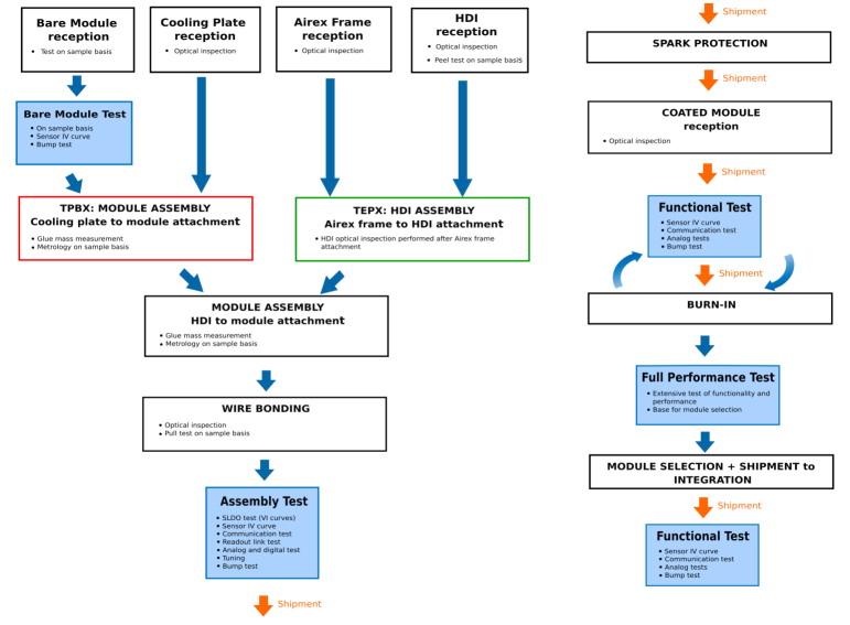
During full-scale production, nearly 4000 pixel modules will be tested. This large number necessitates a stable, efficient, and streamlined measurement procedure, which is designed to be as automated as possible. At each production stage, modules undergo rigorous quality control (QC), including checks for electrical functionality, structural integrity, and thermal stability. Figure 2 illustrates the production flow and the corresponding QC steps.
Initial testing is performed at the bare module level to assess the integrity of the flip-chips prior to assembly. This includes optical inspection of the flip-chips, I-V measurements of the sensors, and low-voltage tests on the readout chips. Once assembled, each module undergoes the Assembly Test, which verifies functionality that may be affected by mechanical assembly steps or wire bonding. Modules that fail to meet the electrical requirements at this stage are excluded from further production steps. Throughout the production process, modules are shipped multiple times, particularly for spark protection and coating. After each shipment, a Functional Test is conducted—most importantly after spark protection and again upon reception at the integration site—to verify that shipping and processing have not affected the module’s performance.
Final qualification is performed during the Full Performance Test, which provides the data used for module selection. Modules are tested both at 17 ∘C and at the nominal operating temperature of -20 ∘C. This test is performed after the burn-in stage, where modules undergo at least 10 thermal cycles between 35 ∘C and +40 ∘C in a dedicated cold box to ensure thermal robustness and long-term stability. Bump bond integrity is re-evaluated after thermal cycling, as the temperature-induced stress can expose weak or marginal bump connections.
3 Bump bonding tests
Bump bonding, also referred to as hybridization, is a critical process in the construction of pixel modules, in which each pixel of the silicon sensor is electrically connected to its corresponding readout pixel on the CROC chip via micro-bumps. This operation demands sub-micron alignment accuracy, uniform bump formation, and reliable thermal compression to ensure high-quality connections. For the CMS Inner Tracker upgrade, hybridization is carried out by specialized industrial partners, including IZM, Advafab, and Micross. Ensuring bond quality is essential, as missing or defective bumps can result in non-functional pixels, degrading tracking performance. To ensure high bump yield throughout production, dedicated qualification procedures have been implemented.
3.1 Crosstalk method
The crosstalk method assesses the integrity of bump bonds between the sensor and the readout chip by utilizing the internal charge injection circuitry of the front-end electronics. A large signal (39,000 e-) is injected into a specific pixel, and the response of neighboring pixels is measured. In the case of a properly connected bump bond, the injected charge induces measurable signals in adjacent pixels due to capacitive coupling. Conversely, if the bump bond is missing, this coupling is suppressed, and neighboring pixels show significantly reduced or no response. This technique is advantageous because it is non-destructive, does not require external radiation sources, and can be easily automated, making it well-suited for use during module production.
To increase the method’s sensitivity, two distinct pixel injection patterns are used: coupled and uncoupled. This distinction arises from the different layout geometries of the sensor and the readout chip. The silicon sensors feature rectangular pixels with a pitch of 25100 , while the CROC readout chip uses a 5050 bump pad pitch [2, 5]. This layout leads to varying spatial relationships between injected and neighboring pixels, resulting in different levels of capacitive coupling. Using both injection patterns improves the robustness of the crosstalk method and helps avoid misclassification of pixels affected by neighboring defects.
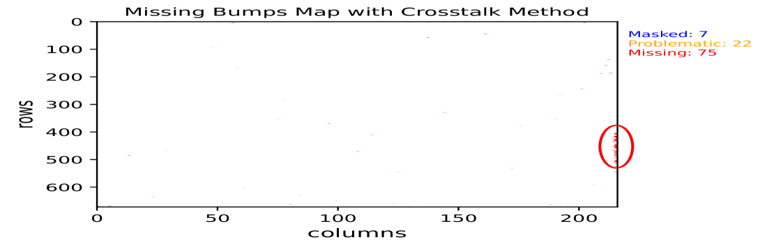
Figure 3(a) illustrates these two configurations: the coupled case (left) shows stronger crosstalk in nearby pixels due to closer proximity, while the uncoupled case (right) results in more isolated signal responses. After injection, the efficiency of signal detection in surrounding pixels is evaluated, as shown in figure 3(b). Pixels with efficiency below 10 for both injection configurations are flagged as missing, those above 95 are considered functional, and the remaining are labeled as problematic. These thresholds were optimized based on studies on prototype modules.
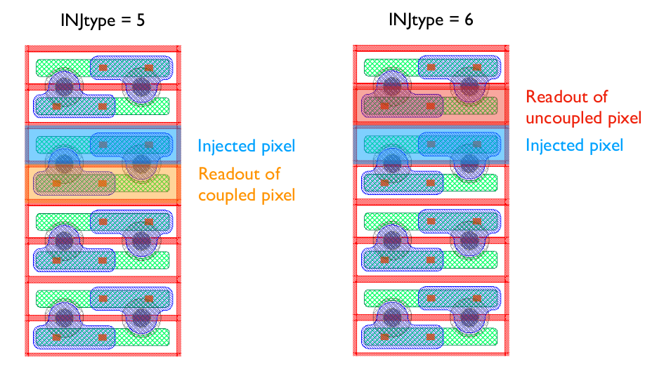
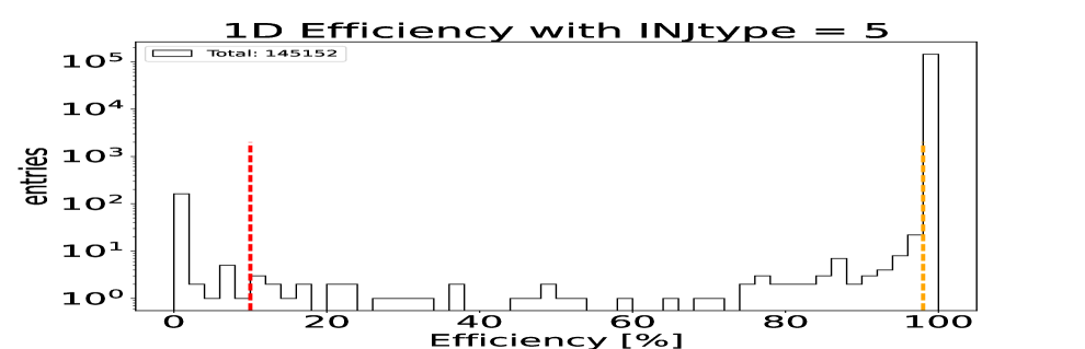
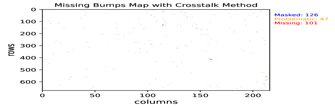
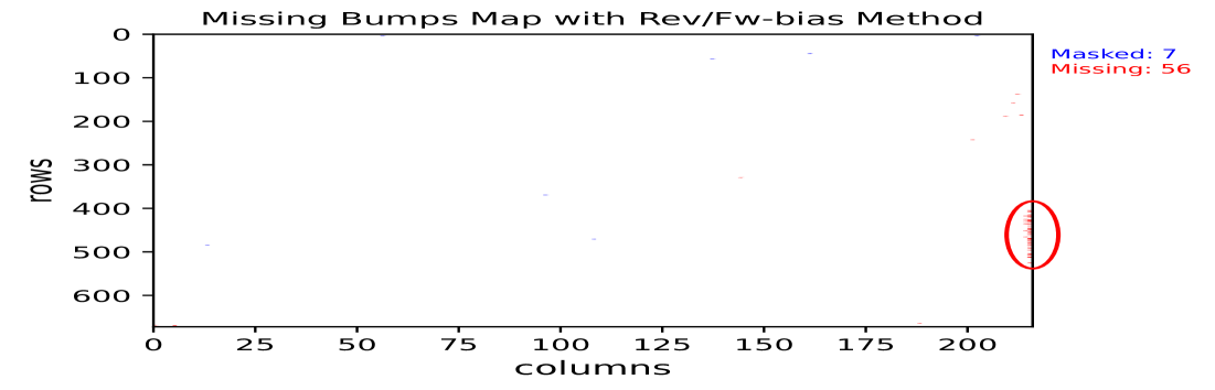
Figure 4 shows the bump bond classification results as an example for a double module with 3D sensors, bump bonded by Advafab and assembled at INFN Firenze. The two flip-chips are mounted on a common high-density interconnect (HDI), and pixels are categorized as masked (blue), problematic (orange), or missing (red) based on their efficiency response to charge injection; all other pixels are considered functional.
3.2 Reverse/Forward bias method
The reverse/forward bias method identifies missing bump bonds by analyzing pixel responses under two sensor bias conditions: reverse bias ( V) and forward bias ( V). In forward bias, a small current is injected into the input of the preamplifier through the sensor. This current modifies the baseline behavior of pixels with intact bump bonds, typically pushing the preamplifier into saturation. In contrast, pixels with missing bumps remain electrically isolated and show little or no change between the two conditions [6].
To assess bump connectivity, the sensor is tuned to a high threshold (around 6000 e-) and S-curve scans are performed under both bias conditions. A high threshold reduces the influence of noise and enhances sensitivity to baseline shifts caused by the injected current. An S-curve describes the efficiency of a pixel as a function of the injected signal amplitude and has a characteristic sigmoid shape. The inflection point corresponds to the pixel’s threshold, while the slope is related to its noise [7, 8]. These parameters are extracted for each pixel and compared between the two settings.
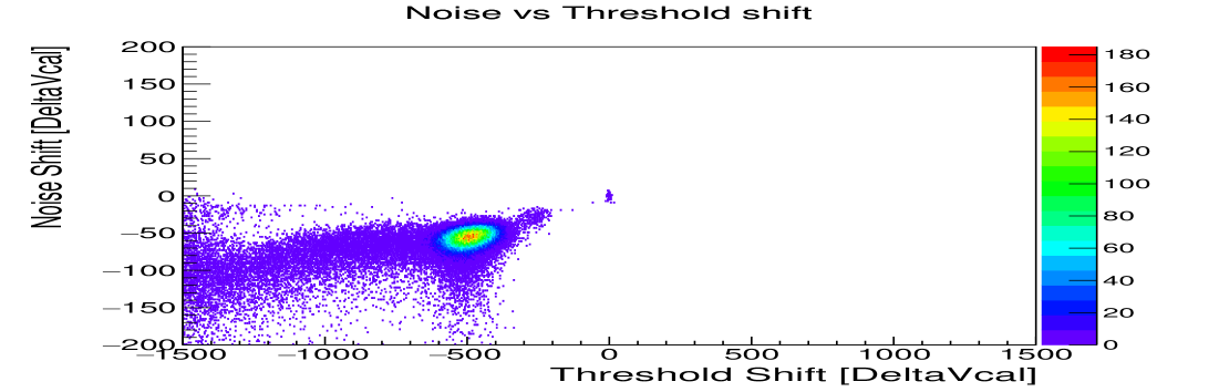
Well-connected pixels typically exhibit a clear shift in threshold and an increase in noise under forward bias. These changes are due to saturation or baseline distortion in the analog front-end. Disconnected pixels, lacking the current injection path, maintain consistent threshold and noise values in both bias modes. The shifts in threshold () and noise () are used to classify bump status. Figure 5 shows 2D distributions of these values for two flip-chips of a double module. Pixels with both shift values below a predefined threshold are flagged as disconnected.
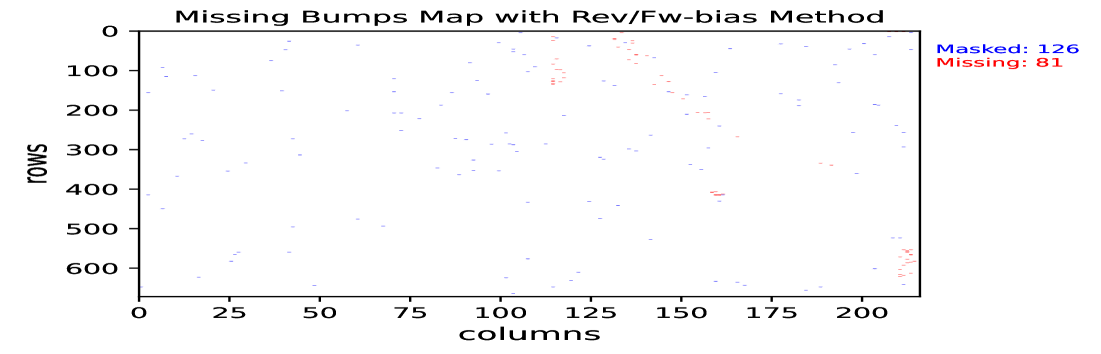
Experimentally, it was observed that reducing the preamplifier bias current enhances the sensitivity of the method. A lower bias current reduces the dynamic range of the analog front-end, making it more susceptible to baseline shifts induced by the current injected under forward bias. This leads to more pronounced changes in threshold and noise for pixels with functional bump bonds. The effect is especially beneficial for planar sensors, where the injected current is relatively small due to geometric factors. In contrast, 3D sensors inject more current and naturally induce larger shifts, making the method effective for them even at higher preamplifier currents. Figure 6 shows the bump bond classification maps derived from this method for both flip-chips of a double module. Pixels identified as missing are shown in red, and masked pixels in blue.

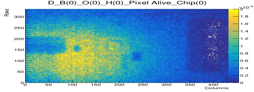
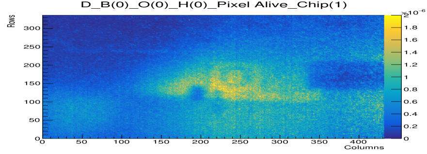
3.3 Beta source imaging
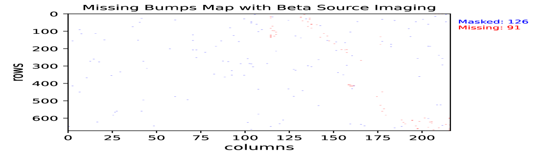
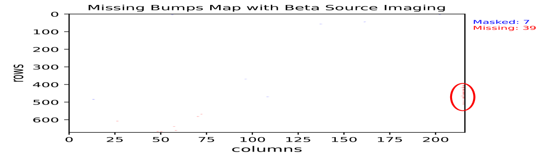
Beta source imaging provides a direct and reliable method for identifying missing bump bonds. In this approach, the module is uniformly irradiated using a 90Sr beta source. Ionization within the silicon sensor generates charge carriers, which are collected by the readout chip through the bump bonds. Prior to irradiation, modules undergo standard calibration procedures, including threshold tuning, noise scans, and pixel masking. Data acquisition is performed with high trigger statistics (typically triggers) to ensure statistical significance. The resulting efficiency maps are then analyzed to identify disconnected pixels, as shown in figures 7 and 8.
Pixels located beneath mechanical structures such as the HDI connector may appear inactive because of shadowing effects that reduce particle flux. To avoid misidentifying these pixels as disconnected, they are excluded from the bump classification map based on their known geometric location. Although this method provides a clear physical confirmation of bump connectivity, it is relatively time-consuming and sensitive to non-uniform exposure. It is therefore used primarily to validate suspicious results from electrical tests or for final cross-checks. When combined with other methods, beta imaging offers high-confidence verification of bump bond integrity.
4 Conclusions
Ensuring high bump bond yield is essential for the CMS Inner Tracker’s performance at the HL-LHC. The methods evaluated in this study probe different physical mechanisms and offer complementary strengths. The crosstalk method is fast, scalable, and applicable to both planar and 3D sensors, making it the default for production, though it may overestimate defects, particularly near sensor edges. The reverse/forward bias method directly assesses electrical continuity and is especially effective for 3D sensors, but is less sensitive in planar sensors due to lower injection current. Beta source imaging offers high-confidence physical confirmation through charge collection but is time-consuming and more sensitive to shadowing and irradiation non-uniformity. It is therefore mainly used to validate critical modules or clarify ambiguous cases.
Table 1 summarizes the number of missing bumps reported by each method for selected prototype flip-chips. The number of ‘matched’ pixels indicates overlap with the crosstalk results. In several cases, the agreement between methods exceeds 70%, particularly for the reverse/forward bias method. However, lower match rates are also observed—especially in beta imaging for specific chips such as FI25 Chip 0—highlighting the distinct sensitivities of each technique. This may be due to partially connected bumps that appear disconnected in electrical tests but still respond under beta irradiation via residual capacitive or AC-like coupling.
| Chip | Crosstalk | Reverse/Forward Bias | Beta Imaging |
|---|---|---|---|
| FI23 Chip 0 | 101 | 81 (77 matched) | 91 (79 matched) |
| FI23 Chip 1 | 75 | 56 (56 matched) | 39 (32 matched) |
| FI24 Chip 0 | 279 | 227 (195 matched) | 236 (175 matched) |
| FI25 Chip 0 | 71 | 43 (30 matched) | 17 (15 matched) |
The developed methods have been successfully validated on prototype modules and are now integrated into the CMS quality control framework. Their combined use provides complementary sensitivity and redundancy, ensuring that only modules with robust bump bonding are selected for final assembly. This comprehensive strategy is crucial for maintaining the tracking performance and long-term reliability of the CMS Inner Tracker throughout HL-LHC operation.
References
- [1] CMS Collaboration, The CMS experiment at the CERN LHC, JINST 3 (2008) S08004.
- [2] CMS Collaboration, The Phase-2 Upgrade of the CMS Tracker, Tech. Rep. CERN-LHCC-2017-009, CMS-TDR-014, CERN, Geneva (2017).
- [3] F. Loddo et al., RD53 pixel chips for the ATLAS and CMS Phase-2 upgrades at HL-LHC, Nucl. Instrum. Meth. A 1067 (2024) 169682.
- [4] CMS Tracker Group collaboration, Powering of the CMS Phase-2 Upgraded Tracker, PoS 370 (2020) 066.
- [5] RD53 collaboration, RD53C Chip Manual, Tech. Rep. CERN-RD53-PUB-24-001, CERN (2024).
- [6] A. Starodumov, W. Erdmann, R. Horisberger, H.C. Kästli, D. Kotlinski, U. Langenegger et al., Qualification procedures of the CMS pixel barrel modules, Nucl. Instrum. Meth. A 565 (2006) 67.
- [7] Y. Ding et al., The study of calibration for the hybrid pixel detector with single photon counting in HEPS-BPIX, IEEE Trans. on Nucl. Sci. 67 (2020) 1812.
- [8] D. Kotliński, Status of the CMS Pixel detector, JINST 4 (2009) P03019.